EP0642919A1 - Produit stratifié et plaque de circuit imprimé multicouche - Google Patents
Produit stratifié et plaque de circuit imprimé multicouche Download PDFInfo
- Publication number
- EP0642919A1 EP0642919A1 EP94110617A EP94110617A EP0642919A1 EP 0642919 A1 EP0642919 A1 EP 0642919A1 EP 94110617 A EP94110617 A EP 94110617A EP 94110617 A EP94110617 A EP 94110617A EP 0642919 A1 EP0642919 A1 EP 0642919A1
- Authority
- EP
- European Patent Office
- Prior art keywords
- resin
- sea
- island
- woven reinforcement
- laminate
- Prior art date
- Legal status (The legal status is an assumption and is not a legal conclusion. Google has not performed a legal analysis and makes no representation as to the accuracy of the status listed.)
- Granted
Links
Images
Classifications
-
- B—PERFORMING OPERATIONS; TRANSPORTING
- B32—LAYERED PRODUCTS
- B32B—LAYERED PRODUCTS, i.e. PRODUCTS BUILT-UP OF STRATA OF FLAT OR NON-FLAT, e.g. CELLULAR OR HONEYCOMB, FORM
- B32B5/00—Layered products characterised by the non- homogeneity or physical structure, i.e. comprising a fibrous, filamentary, particulate or foam layer; Layered products characterised by having a layer differing constitutionally or physically in different parts
- B32B5/22—Layered products characterised by the non- homogeneity or physical structure, i.e. comprising a fibrous, filamentary, particulate or foam layer; Layered products characterised by having a layer differing constitutionally or physically in different parts characterised by the presence of two or more layers which are next to each other and are fibrous, filamentary, formed of particles or foamed
- B32B5/24—Layered products characterised by the non- homogeneity or physical structure, i.e. comprising a fibrous, filamentary, particulate or foam layer; Layered products characterised by having a layer differing constitutionally or physically in different parts characterised by the presence of two or more layers which are next to each other and are fibrous, filamentary, formed of particles or foamed one layer being a fibrous or filamentary layer
- B32B5/26—Layered products characterised by the non- homogeneity or physical structure, i.e. comprising a fibrous, filamentary, particulate or foam layer; Layered products characterised by having a layer differing constitutionally or physically in different parts characterised by the presence of two or more layers which are next to each other and are fibrous, filamentary, formed of particles or foamed one layer being a fibrous or filamentary layer another layer next to it also being fibrous or filamentary
-
- B—PERFORMING OPERATIONS; TRANSPORTING
- B32—LAYERED PRODUCTS
- B32B—LAYERED PRODUCTS, i.e. PRODUCTS BUILT-UP OF STRATA OF FLAT OR NON-FLAT, e.g. CELLULAR OR HONEYCOMB, FORM
- B32B27/00—Layered products comprising a layer of synthetic resin
- B32B27/12—Layered products comprising a layer of synthetic resin next to a fibrous or filamentary layer
-
- B—PERFORMING OPERATIONS; TRANSPORTING
- B32—LAYERED PRODUCTS
- B32B—LAYERED PRODUCTS, i.e. PRODUCTS BUILT-UP OF STRATA OF FLAT OR NON-FLAT, e.g. CELLULAR OR HONEYCOMB, FORM
- B32B5/00—Layered products characterised by the non- homogeneity or physical structure, i.e. comprising a fibrous, filamentary, particulate or foam layer; Layered products characterised by having a layer differing constitutionally or physically in different parts
- B32B5/02—Layered products characterised by the non- homogeneity or physical structure, i.e. comprising a fibrous, filamentary, particulate or foam layer; Layered products characterised by having a layer differing constitutionally or physically in different parts characterised by structural features of a fibrous or filamentary layer
- B32B5/024—Woven fabric
-
- C—CHEMISTRY; METALLURGY
- C08—ORGANIC MACROMOLECULAR COMPOUNDS; THEIR PREPARATION OR CHEMICAL WORKING-UP; COMPOSITIONS BASED THEREON
- C08J—WORKING-UP; GENERAL PROCESSES OF COMPOUNDING; AFTER-TREATMENT NOT COVERED BY SUBCLASSES C08B, C08C, C08F, C08G or C08H
- C08J5/00—Manufacture of articles or shaped materials containing macromolecular substances
- C08J5/24—Impregnating materials with prepolymers which can be polymerised in situ, e.g. manufacture of prepregs
- C08J5/241—Impregnating materials with prepolymers which can be polymerised in situ, e.g. manufacture of prepregs using inorganic fibres
- C08J5/244—Impregnating materials with prepolymers which can be polymerised in situ, e.g. manufacture of prepregs using inorganic fibres using glass fibres
-
- C—CHEMISTRY; METALLURGY
- C08—ORGANIC MACROMOLECULAR COMPOUNDS; THEIR PREPARATION OR CHEMICAL WORKING-UP; COMPOSITIONS BASED THEREON
- C08J—WORKING-UP; GENERAL PROCESSES OF COMPOUNDING; AFTER-TREATMENT NOT COVERED BY SUBCLASSES C08B, C08C, C08F, C08G or C08H
- C08J5/00—Manufacture of articles or shaped materials containing macromolecular substances
- C08J5/24—Impregnating materials with prepolymers which can be polymerised in situ, e.g. manufacture of prepregs
- C08J5/246—Impregnating materials with prepolymers which can be polymerised in situ, e.g. manufacture of prepregs using polymer based synthetic fibres
-
- C—CHEMISTRY; METALLURGY
- C08—ORGANIC MACROMOLECULAR COMPOUNDS; THEIR PREPARATION OR CHEMICAL WORKING-UP; COMPOSITIONS BASED THEREON
- C08J—WORKING-UP; GENERAL PROCESSES OF COMPOUNDING; AFTER-TREATMENT NOT COVERED BY SUBCLASSES C08B, C08C, C08F, C08G or C08H
- C08J5/00—Manufacture of articles or shaped materials containing macromolecular substances
- C08J5/24—Impregnating materials with prepolymers which can be polymerised in situ, e.g. manufacture of prepregs
- C08J5/249—Impregnating materials with prepolymers which can be polymerised in situ, e.g. manufacture of prepregs characterised by the additives used in the prepolymer mixture
-
- H—ELECTRICITY
- H05—ELECTRIC TECHNIQUES NOT OTHERWISE PROVIDED FOR
- H05K—PRINTED CIRCUITS; CASINGS OR CONSTRUCTIONAL DETAILS OF ELECTRIC APPARATUS; MANUFACTURE OF ASSEMBLAGES OF ELECTRICAL COMPONENTS
- H05K1/00—Printed circuits
- H05K1/02—Details
- H05K1/03—Use of materials for the substrate
- H05K1/0313—Organic insulating material
- H05K1/0353—Organic insulating material consisting of two or more materials, e.g. two or more polymers, polymer + filler, + reinforcement
- H05K1/0366—Organic insulating material consisting of two or more materials, e.g. two or more polymers, polymer + filler, + reinforcement reinforced, e.g. by fibres, fabrics
-
- H—ELECTRICITY
- H10—SEMICONDUCTOR DEVICES; ELECTRIC SOLID-STATE DEVICES NOT OTHERWISE PROVIDED FOR
- H10W—GENERIC PACKAGES, INTERCONNECTIONS, CONNECTORS OR OTHER CONSTRUCTIONAL DETAILS OF DEVICES COVERED BY CLASS H10
- H10W70/00—Package substrates; Interposers; Redistribution layers [RDL]
- H10W70/60—Insulating or insulated package substrates; Interposers; Redistribution layers
- H10W70/67—Insulating or insulated package substrates; Interposers; Redistribution layers characterised by their insulating layers or insulating parts
- H10W70/69—Insulating materials thereof
- H10W70/695—Organic materials
-
- B—PERFORMING OPERATIONS; TRANSPORTING
- B32—LAYERED PRODUCTS
- B32B—LAYERED PRODUCTS, i.e. PRODUCTS BUILT-UP OF STRATA OF FLAT OR NON-FLAT, e.g. CELLULAR OR HONEYCOMB, FORM
- B32B2260/00—Layered product comprising an impregnated, embedded, or bonded layer wherein the layer comprises an impregnation, embedding, or binder material
- B32B2260/02—Composition of the impregnated, bonded or embedded layer
- B32B2260/021—Fibrous or filamentary layer
-
- B—PERFORMING OPERATIONS; TRANSPORTING
- B32—LAYERED PRODUCTS
- B32B—LAYERED PRODUCTS, i.e. PRODUCTS BUILT-UP OF STRATA OF FLAT OR NON-FLAT, e.g. CELLULAR OR HONEYCOMB, FORM
- B32B2260/00—Layered product comprising an impregnated, embedded, or bonded layer wherein the layer comprises an impregnation, embedding, or binder material
- B32B2260/04—Impregnation, embedding, or binder material
- B32B2260/046—Synthetic resin
-
- B—PERFORMING OPERATIONS; TRANSPORTING
- B32—LAYERED PRODUCTS
- B32B—LAYERED PRODUCTS, i.e. PRODUCTS BUILT-UP OF STRATA OF FLAT OR NON-FLAT, e.g. CELLULAR OR HONEYCOMB, FORM
- B32B2457/00—Electrical equipment
- B32B2457/08—PCBs, i.e. printed circuit boards
-
- B—PERFORMING OPERATIONS; TRANSPORTING
- B32—LAYERED PRODUCTS
- B32B—LAYERED PRODUCTS, i.e. PRODUCTS BUILT-UP OF STRATA OF FLAT OR NON-FLAT, e.g. CELLULAR OR HONEYCOMB, FORM
- B32B2509/00—Household appliances
-
- B—PERFORMING OPERATIONS; TRANSPORTING
- B32—LAYERED PRODUCTS
- B32B—LAYERED PRODUCTS, i.e. PRODUCTS BUILT-UP OF STRATA OF FLAT OR NON-FLAT, e.g. CELLULAR OR HONEYCOMB, FORM
- B32B2605/00—Vehicles
- B32B2605/08—Cars
-
- H—ELECTRICITY
- H05—ELECTRIC TECHNIQUES NOT OTHERWISE PROVIDED FOR
- H05K—PRINTED CIRCUITS; CASINGS OR CONSTRUCTIONAL DETAILS OF ELECTRIC APPARATUS; MANUFACTURE OF ASSEMBLAGES OF ELECTRICAL COMPONENTS
- H05K1/00—Printed circuits
- H05K1/02—Details
- H05K1/03—Use of materials for the substrate
- H05K1/0313—Organic insulating material
- H05K1/0353—Organic insulating material consisting of two or more materials, e.g. two or more polymers, polymer + filler, + reinforcement
- H05K1/0373—Organic insulating material consisting of two or more materials, e.g. two or more polymers, polymer + filler, + reinforcement containing additives, e.g. fillers
-
- H—ELECTRICITY
- H05—ELECTRIC TECHNIQUES NOT OTHERWISE PROVIDED FOR
- H05K—PRINTED CIRCUITS; CASINGS OR CONSTRUCTIONAL DETAILS OF ELECTRIC APPARATUS; MANUFACTURE OF ASSEMBLAGES OF ELECTRICAL COMPONENTS
- H05K2201/00—Indexing scheme relating to printed circuits covered by H05K1/00
- H05K2201/01—Dielectrics
- H05K2201/0137—Materials
- H05K2201/015—Fluoropolymer, e.g. polytetrafluoroethylene [PTFE]
-
- H—ELECTRICITY
- H05—ELECTRIC TECHNIQUES NOT OTHERWISE PROVIDED FOR
- H05K—PRINTED CIRCUITS; CASINGS OR CONSTRUCTIONAL DETAILS OF ELECTRIC APPARATUS; MANUFACTURE OF ASSEMBLAGES OF ELECTRICAL COMPONENTS
- H05K2201/00—Indexing scheme relating to printed circuits covered by H05K1/00
- H05K2201/02—Fillers; Particles; Fibers; Reinforcement materials
- H05K2201/0203—Fillers and particles
- H05K2201/0206—Materials
- H05K2201/0209—Inorganic, non-metallic particles
-
- H—ELECTRICITY
- H05—ELECTRIC TECHNIQUES NOT OTHERWISE PROVIDED FOR
- H05K—PRINTED CIRCUITS; CASINGS OR CONSTRUCTIONAL DETAILS OF ELECTRIC APPARATUS; MANUFACTURE OF ASSEMBLAGES OF ELECTRICAL COMPONENTS
- H05K2201/00—Indexing scheme relating to printed circuits covered by H05K1/00
- H05K2201/02—Fillers; Particles; Fibers; Reinforcement materials
- H05K2201/0203—Fillers and particles
- H05K2201/0206—Materials
- H05K2201/0212—Resin particles
-
- H—ELECTRICITY
- H05—ELECTRIC TECHNIQUES NOT OTHERWISE PROVIDED FOR
- H05K—PRINTED CIRCUITS; CASINGS OR CONSTRUCTIONAL DETAILS OF ELECTRIC APPARATUS; MANUFACTURE OF ASSEMBLAGES OF ELECTRICAL COMPONENTS
- H05K2201/00—Indexing scheme relating to printed circuits covered by H05K1/00
- H05K2201/02—Fillers; Particles; Fibers; Reinforcement materials
- H05K2201/0275—Fibers and reinforcement materials
- H05K2201/029—Woven fibrous reinforcement or textile
-
- H—ELECTRICITY
- H05—ELECTRIC TECHNIQUES NOT OTHERWISE PROVIDED FOR
- H05K—PRINTED CIRCUITS; CASINGS OR CONSTRUCTIONAL DETAILS OF ELECTRIC APPARATUS; MANUFACTURE OF ASSEMBLAGES OF ELECTRICAL COMPONENTS
- H05K2201/00—Indexing scheme relating to printed circuits covered by H05K1/00
- H05K2201/06—Thermal details
- H05K2201/068—Thermal details wherein the coefficient of thermal expansion is important
Definitions
- the present invention relates to a laminate and a multilayer printed circuit board on each of which semiconductor elements can be mounted.
- Multilayer substrates of low thermal expansibilities include a substrate having a ceramics core layer, a substrate with ceramics deposited on a copper foil by flame spraying, and so forth.
- the coefficients of thermal expansion of these substrates are 10 [ppm/K] or less in the planar directions thereof (in the direction of each substrate within the bonding surface thereof).
- the ceramics-based substrates are problematic in their drillabilities in the case of forming through-holes.
- organic substance based substrates it has been known that the coefficient of thermal expansion can be reduced by mixing an inorganic filler into a resin system. This contrivance, however, results in enlarging the elastic modulus of the substrate and is not always satisfactory for attaining lower stresses.
- the present invention has for its object to provide a laminate, a multilayer printed circuit board and a prepreg each of which exhibits low thermal stresses owing to a small thermal expansion coefficient and a low elastic modulus, and electronics products employing any of them.
- the first of the expedients is a laminate capable of mounting semiconductor elements thereon; comprising an insulating layer which is constituted by a resin portion of sea-island structure and a woven reinforcement, and which exhibits a coefficient of thermal expansion of 3.0 ⁇ 10 [ppm/K] in a planar direction thereof and a glass transition temperature of 150 ⁇ 300 [°C].
- the second expedient is a multilayer printed circuit board capable of mounting semiconductor elements thereon; comprising at least two insulating layers each of which is constituted by a resin portion of sea-island structure and a woven reinforcement, and each of which exhibits a coefficient of thermal expansion of 3.0 ⁇ 10 [ppm/K] in a planar direction thereof and a glass transition temperature of 150 ⁇ 300 [°C].
- the third expedient is a laminate capable of mounting semiconductor elements thereon; comprising an insulating layer which is constituted by a resin portion of sea-island structure, an inorganic filler and a woven reinforcement, and which exhibits a coefficient of thermal expansion of 3.0 ⁇ 10 [ppm/K] in a planar direction thereof and a glass transition temperature of 150 ⁇ 300 [°C].
- the fourth expedient is a multilayer printed circuit board capable of mounting semiconductor elements thereon; comprising at least two insulating layers each of which is constituted by a resin portion of sea-island structure, an inorganic filler and a woven reinforcement, and each of which exhibits a coefficient of thermal expansion of 3.0 ⁇ 10 [ppm/K] in a planar direction thereof and a glass transition temperature of 150 ⁇ 300 [°C].
- the fifth expedient is a prepreg wherein a woven reinforcement is impregnated with a resin component; comprising the fact that said resin component includes a resin portion of sea-island structure, and that the prepreg after having been set exhibits a coefficient of thermal expansion of 3.0 ⁇ 10 [ppm/K] in a planar direction thereof and a glass transition temperature of 150 ⁇ 300 [°C].
- the sixth expedient is a prepreg wherein a woven reinforcement is impregnated with a resin component; comprising the fact that said resin component includes a resin portion of sea-island structure and an inorganic filler at an average grain diameter of 0.1 ⁇ 15 [ ⁇ m], and that the prepreg after having been set exhibits a coefficient of thermal expansion of 3.0 ⁇ 10 [ppm/K] in a planar direction thereof and a glass transition temperature of 150 ⁇ 300 [°C].
- the seventh expedient is a memory card wherein a memory element is mounted on a circuit board by surface packaging; comprising the fact that said circuit board includes an insulating layer which is constituted by a resin portion of sea-island structure and a woven reinforcement, and which exhibits a coefficient of thermal expansion of 3.0 ⁇ 10 [ppm/K] in a planar direction thereof and a glass transition temperature of 150 ⁇ 300 [°C].
- the eighth expedient is a computer which has a multilayer printed circuit board capable of mounting semiconductor elements thereon; comprising the fact that said multilayer printed circuit board includes an insulating layer which is constituted by a resin portion of sea-island structure and a woven reinforcement, and which exhibits a coefficient of thermal expansion of 3.0 ⁇ 10 [ppm/K] in a planar direction thereof and a glass transition temperature of 150 ⁇ 300 [°C], and that a signal transmission delay time of said computer is 1 ⁇ 15 [ns/m].
- the ninth expedient is a communication equipment which has a circuit board capable of mounting semiconductor elements thereon; comprising the fact that said circuit board includes an insulating layer which is constituted by a resin portion of sea-island structure and a woven reinforcement, and which exhibits a coefficient of thermal expansion of 3.0 ⁇ 10 [ppm/K] in a planar direction thereof and a glass transition temperature of 150 ⁇ 300 [°C], and that a weight of said communication equipment is 10 [g] ⁇ 30 [kg].
- the tenth expedient is an electronics equipment which has a circuit board capable of mounting semiconductor elements thereon; comprising the fact that said circuit board includes an insulating layer which is constituted by a resin portion of sea-island structure and a woven reinforcement, and which exhibits a coefficient of thermal expansion of 3.0 ⁇ 10 [ppm/K] in a planar direction thereof and a glass transition temperature of 150 ⁇ 300 [°C], and that a total volume occupied by said semiconductor elements and said circuit board is 1 ⁇ 50 [%] with respect to a volume of the whole electronics equipment.
- the eleventh expedient is a laminate wherein at least one prepreg or sheet which is constituted by a resin and a woven reinforcement is stacked and bonded; comprising the fact that said woven reinforcement is constructed so as to exhibit an anisotropy as a physical property, and that said resin is in the form of a continuous layer which has a sea-island structure and which prevents the layers of woven reinforcement from coming into contact with each other.
- the twelfth expedient is a laminate wherein at least one prepreg or sheet which is constituted by a resin and a woven reinforcement is stacked and bonded; comprising the fact that said woven reinforcement is constructed so as to exhibit an anisotropy as a physical property, that said resin is in the form of a continuous layer which has a sea-island structure and which prevents the layers of woven reinforcement from coming into contact with each other, and that said laminate exhibits a coefficient of thermal expansion of 3.0 ⁇ 10 [ppm/K] in a planar direction thereof and a glass transition temperature of 150 ⁇ 300 [°C].
- a "semiconductor element” is an element in which an IC (integrated circuit) or LSI (large-scale integrated circuit) including, for example, a memory, a logic circuit, a custom IC or/and a power transistor is formed on a wafer made of a semiconductor such as Si (silicon) or GaAs (gallium arsenide), and which has terminals for connecting the IC or LSI to leads, bumps etc.
- the elements shall include, not only bare chips, but also packaged chips in the state in which the element is covered or encapsulated with a resin or ceramics, in the state in which the element has been subjected to tape automatic bonding (TAB), and so forth.
- a "laminate” is a structural product or member which is fabricated in such a way that at least one piece of prepreg, sheet or the like which has been obtained by impregnating a woven reinforcement with a resin component is layered, and that the layer is pressed, bonded and molded.
- the woven reinforcements include a piece of cloth or sheet which is made of inorganic type fiber glass of (such as E glass (electrical glass), S glass (structural glass), D glass (dielectric glass) or Q glass (quartz glass)), titanium or the like; a piece of cloth or sheet which is made of organic type fiber of polyamide, polyamidoimide, polyimide, a liquid-crystalline polymer, aromatic polyamide or the like; a piece of cloth which is made of carbon fiber; and a piece of cloth or sheet which is made of at least two kinds of fiber selected from among the inorganic type fiber, organic type fibers and carbon fibers mentioned above.
- inorganic type fiber glass of such as E glass (electrical glass), S glass (structural glass), D glass (dielectric glass) or Q glass (quartz glass)
- titanium or the like a piece of cloth or sheet which is made of organic type fiber of polyamide, polyamidoimide, polyimide, a liquid-crystalline polymer, aromatic polyamide or the like
- a "multilayer printed circuit board” is a wired circuit board for mounting semiconductor elements thereon, which is formed with at least two wiring layers that are connected by means of through-holes etc.
- the wiring layers bear circuits which are formed from foils of metals or by plating with or vacuum evaporation of metals.
- the metals are copper, silver, gold, aluminum, chromium, molybdenum, tungsten, etc. Especially, copper is preferable, and the copper foil is recommended.
- a resinous varnish for impregnating the woven reinforcement in the present invention accounts for about 30 ⁇ 90 [weight-%] in terms of the solid matter content of the varnish with respect to the total weight of both the varnish and the woven reinforcement (that is, the woven reinforcement accounts for about 70 ⁇ 10 [weight-%] with respect to the total weight).
- the proportion of the varnish is smaller, a good prepreg or film is difficult to obtain.
- the proportion of the varnish is larger, it is difficult to make the coefficient of thermal expansion of the laminate in the planar direction thereof fall within a range of 3.0 ⁇ 10 [ppm/K]. Besides, the effect of reinforcing the laminate decreases.
- the laminate according to the present invention is well suited to wiring uses such as, for example, a flexible wiring circuit board and an insulating film to intervene between circuits.
- the flexible wiring circuit board is manufactured as stated below.
- a piece of glass cloth is impregnated with a varnish which has been prepared by dissolving a resin composite in an organic solvent.
- a setting reaction is somewhat advanced to form a prepreg at B-stage (in the semi-set state in which the prepreg melts when heat is applied thereto).
- metal foils such as copper foils or aluminum foils are superposed on both the surfaces of the prepreg so as to sandwich the prepreg therebetween.
- such a metal foil is superposed on only one surface of the prepreg. In this state, each metal foil is bonded by thermocompression, and the impregnating resin composite is set at the same time.
- the surface of the metal foil (copper foil) is coated with resist ink in the shape of a circuit, and the resist ink is dried.
- the parts of the copper foil except the circuit are etched with, e. g., an aqueous solution of ferric chloride.
- an organic solvent such as methylene chloride, the resist ink is removed, and the resulting structure is washed.
- the resulting structure is dipped into a soldering bath so as to stick solder to pertinent parts. Then, the circuit is finished.
- the flexible substrate or flexible circuit board of the present invention is generally put on the market in the semi-set state (as the prepreg) or in the set state after the thermocompression bonding of the metal foil or foils.
- the flexible substrate or circuit board in the present invention shall include articles in both the semi-set state and the set state.
- the multilayer printed circuit board according to the present invention can also be fabricated as stated below.
- a printed-wiring circuit board already formed with a circuit is coated with a varnish prepared by dissolving a resin component in a solvent.
- the varnish is somewhat set into the B-stage (into the semi-set state).
- a metal foil such as copper foil or aluminum foil is superposed on the outer surface of the semi-set resin component, and thermocompression is carried out to bond the metal foil and set the resin component.
- another circuit is formed by the necessary steps of the method explained above.
- the impregnation of a woven reinforcement with a resin can be effected in such a way that a resin solution (varnish) is applied to the woven reinforcement once or a plurality of times by the use of a conventional impregnating-and-coating machine of horizontal type or/and vertical type.
- the impregnating process can be performed by coating one surface or both surfaces of the woven reinforcement with the resin.
- the impregnating process can be performed in such a way that a solid resin sheet is superposed on the woven reinforcement beforehand, and that the resulting woven reinforcement is heated and/or molded.
- a mold releasing sheet can be used voluntarily at a suitable step.
- the mold releasing sheet is cellulosic paper or film coated with a mold releasing agent, polypropylene film, polyvinyl alcohol film, or the like.
- a "resin portion of sea-island structure” is made from a resin composite which consists of at least two kinds of substances (e. g., a resin and a compound, or resins) being inferiorly miscible to each other, or from a resin composite which contains a resin of phase separation type, such as a polymer produced by copolymerizing components of inferior miscibility.
- a resin composite which contains a resin of phase separation type, such as a polymer produced by copolymerizing components of inferior miscibility.
- one component should desirably have a lower elastic modulus than the other component or components.
- the resin composite to be selected and used is a composite which has the sea-island structure and in which at least one of components conjointly employed is immiscible with the other component or components.
- thermosetting resins for example, an epoxy resin, an unsaturated polyester resin, an epoxy - isocyanate resin, a maleimide resin, a maleimide - epoxy resin, a cyanate ester resin, a cyanate ester - epoxy resin, a cyanate ester - maleimide resin, a phenolic resin, a diallylphthalate resin, an urethane resin, a cyanamide resin and a maleimide - cyanamide resin.
- an epoxy resin an unsaturated polyester resin
- an epoxy - isocyanate resin for example, an epoxy resin, an unsaturated polyester resin, an epoxy - isocyanate resin, a maleimide resin, a maleimide - epoxy resin, a cyanate ester resin, a cyanate ester - epoxy resin, a cyanate ester - maleimide resin, a phenolic resin, a diallylphthalate resin, an urethane resin, a cyanamide resin and a maleimi
- silicon-containing compounds, fluorine-containing compounds, and the polymers of these compounds are mentioned as the compounds and resins which are immiscible with the aforementioned thermosetting resins and which form the sea-island structures when mixed with these thermosetting resins.
- Typical examples of the silicon-containing compounds are organosiloxane and organopolysiloxane each of which has at its terminals or its side chains, functional groups such as amino groups, carboxyl groups, epoxy groups, hydroxyl groups, pyrimidinyl groups or carboxylic groups.
- fluorine-containing compounds are perfluoroether, PTFE (polytetrafluoroethylene), PFA (tetrafluoroethylene perfluoroalkyl vinyl ether copolymer), FEP (tetrafluoroethylene hexafluoropropene copolymer), PCTFE (polychlorotrifluoroethylene), ETFE (ethylene tetrafluoroethylene copolymer), ECTFE (ethylene chlorotrifluoroethylene copolymer), PVDF (polyvinylidene difluoride) and PVF (polyvinyl fluoride) each of which has at its terminals or its side chains, functional groups such as amino groups, carboxyl groups, epoxy groups, hydroxyl groups, pyrimidinyl groups, isocyanic groups or carboxylic groups.
- Each of the polymers of the specified compounds should preferably have a molecular weight of 103 ⁇ 106. Such a polymer is effective to lower the elastic modulus.
- the aforementioned resin composites of high heat resistances are especially favorable in order that the insulating layer of a laminate or a multilayer printed circuit board, a prepreg, etc. may exhibit glass transition temperatures falling within a range of 150 ⁇ 300 [°C] (the reasons for the specified range will be explained below).
- the aspect of the immiscibility may be either of a nonreactive type or a reactive type, but the reactive type is favorable from the viewpoint of bestowing the high heat resistances.
- the silicon-containing compound and the epoxy compound which have groups being reactive with epoxy groups or hydroxyl groups can be previously reacted in a solution at the preparation of a varnish.
- a setting agent, an inorganic filler and/or a coupling agent it is also possible to add a setting agent, an inorganic filler and/or a coupling agent.
- the glass transition temperature of the insulating layer should preferably fall within the range of 150 ⁇ 300 [°C].
- a glass transition temperature below 150 [°C] it becomes difficult to satisfactorily clear the reliability tests (for example, a high-temperature shelf test and a heat cycle test) of the product such as the laminate or the multilayer printed circuit board.
- the bestowal of the flexibility is difficult, so that the problems of cracking and inferior molding characteristics are involved in the product.
- the "coefficient of thermal expansion in a planar direction” signifies the coefficient of thermal expansion within a bonding surface in a laminate. More specifically, there are three sorts of thermal expansion coefficients within the bonding surface of the laminate.
- the direction in which a tension acts on a woven reinforcement at the step of coating in the manufacture of a prepreg, is assumed an X-direction.
- the direction which is orthogonal to the X-direction is assumed to be a Y-direction.
- the direction which is 45 [degrees] slant to the X- and Y-directions is assumed to be a bias direction.
- the magnitudes of the coefficients of thermal expansion are in the order of the bias direction > the Y-direction > the X-direction.
- the bias direction which is 45 [degrees] slant, the woven reinforcement and the step of stacking and bonding the prepreg exert the least influences.
- the coefficient of thermal expansion in the bias direction shall be representatively stipulated as the coefficient of thermal expansion in the planar direction.
- the coefficient of thermal expansion in the planar direction should preferably fall within a range of 3.0 ⁇ 10 [ppm/K].
- the coefficient of thermal expansion of a semiconductor element (for example, made from silicon) is 3.0 ⁇ 4.0 [ppm/K].
- the coefficient of thermal expansion of an encapsulating resin in a resin-molded semiconductor device is, only slightly greater than the value of silicon. In order to enhance the reliability of the connections between the semiconductor element and a laminate (or a multilayer printed circuit board), it is effective to reduce thermal stresses which arise between both the members or articles.
- the difference between the thermal expansion coefficients of the laminate and the semiconductor element can be rendered small in such a way that the coefficient of thermal expansion of the laminate (or the multilayer printed circuit board) in the planar direction thereof is brought into the range of 3.0 ⁇ 10 [ppm/K].
- the construction of the multilayer printed circuit board according to the present invention does not include ceramics as its constituent, it can lower the coefficient of thermal expansion. Accordingly, the following effects are brought forth:
- various electrical parts such as semiconductor elements can be mounted by surface packaging by employing a circuit board which is constituted by a resin portion and a woven reinforcement, the resin portion having a sea-island structure and exhibiting a coefficient of thermal expansion of 3.0 ⁇ 10 [ppm/K] in a planar direction thereof, as well as a glass transition temperature of 150 ⁇ 300 [°C].
- the circuit board is superior in drillability to a ceramics-containing substrate which is a prior-art substrate of low thermal expansion for the surface packaging, and it is very effective for the reliability of through-holes because the close adhesion thereof with a plated metal is more intense than that of ceramics.
- a ceramics-based circuit board is less bondable with a resin, and it therefore poses a problem with regard to the reliability of the interface between the circuit board and the resin.
- circuit board according to the present invention does not contain ceramics, and the sea-island structure of its resin portion results in a lower elastic modulus compared with an unmodified state. Therefore, even when various electrical parts having unequal thermal expansion coefficients are to be mounted together on the circuit board, thermal stresses which arise at a mounting step are of small magnitude. It is accordingly possible to provide a multifunctional memory card of superior connection reliability.
- the thermal expansion coefficient of a thin package for semiconductor elements of high integration density is nearly equal to that of silicon and is 6 [ppm/K] or so.
- the semiconductor elements of high integration density having low thermal expansion coefficients are therefore permitted to be mounted densely by surface packaging while the connection reliability is kept high, by employing a circuit board which is constituted by a resin portion and a woven reinforcement, the resin portion having a sea-island structure and exhibiting a coefficient of thermal expansion of 3.0 ⁇ 10 [ppm/K] in a planar direction thereof, as well as a glass transition temperature of 150 ⁇ 300 [°C].
- signal transmission distances can be shortened, and a computer of high arithmetic processing speed in which signal transmission delay times are 1 ⁇ 15 [ns/m] can be provided.
- a computer of superior portability can be provided.
- a reduced size and a lightened weight of 10 [g] ⁇ 30 [kg] can be attained to provide a communication equipment of superior portability in such a way that electrical parts such as semiconductor elements are mounted at a high integration density by surface packaging, by employing a circuit board which is constituted by a resin portion and a woven reinforcement, the resin portion having a sea-island structure and exhibiting a coefficient of thermal expansion of 3.0 ⁇ 10 [ppm/K] in a planar direction thereof, as well as a glass transition temperature of 150 ⁇ 300 [°C].
- Typical examples of the communication equipment are a portable telephone set and a portable radio equipment.
- the sea-island substrate is lighter in weight than a ceramics-containing substrate.
- a car electronics equipment including electrical parts such as semiconductor elements, which equipment can reduce the occupying volume of its packaging portion (concretely, a total volume to be occupied by the semiconductor elements and a circuit board can be made 1 ⁇ 50 [%] with respect to the volume of the whole electronics equipment) and can endure a high-temperature and high-humidity environment such as an engine room, in such a way that the electrical parts such as semiconductor elements are mounted at a high integration density by surface packaging, by employing the circuit board which is constituted by a resin portion and a woven reinforcement, the resin portion having a sea-island structure and exhibiting a coefficient of thermal expansion of 3.0 ⁇ 10 [ppm/K] in a planar direction thereof, as well as a glass transition temperature of 150 ⁇ 300 [°C].
- Typical examples of such a car electronics equipment are an engine control device and a navigation device. It is necessary for these devices to be installed in limited places having severe environmental conditions. To this end, the equipment which employs the circuit board constituted by the resin portion of the sea-island structure can achieve a reduced size by the dense packaging. Moreover, since the circuit board does not contain any ceramics material, it has few interfaces of different phases and exhibits a superior connection reliability. Accordingly, the circuit board is well suited for use in the field of car electronics.
- the present invention puts the components of a resin composite into a sea-island structure, namely, a phase separation structure, whereby the thermal expansion coefficient and elastic modulus of the resin composite can be simultaneously reduced.
- a phase separation structure As an example of a mechanism far the manifestation of the phase separation structure, in a case where the phase separation resin of the resin composite has an island structure of low elastic modulus, the resin of the resin composite as a matrix layer will have its elastic modulus reduced owing to a moldability added by the island parts of the island structure.
- a piece of E-glass (electrical glass) cloth 100 [ ⁇ m] thick was impregnated and coated with the varnish, and then dried at 120 [°C] for 10 [min] so as to remove the solvent.
- the resin content of the obtained prepreg was 70 [weight-%].
- Copper foils (each being 18 [ ⁇ m] thick) were respectively superposed on both the surfaces of the obtained prepreg, and the resulting structure was pressed under heat by a press. Thus, a laminate was obtained.
- two-stage reactions at 130 [°C] for 30 [min] and at 180 [°C] for 60 [min] were performed, and a pressure of 196.2 N/cm2 (20 [kg/cm2]) was held.
- the copper foil peeling strength of the obtained laminate, and the thermal expansion coefficient of the laminate in the planar direction thereof after having etched the copper foils were evaluated by the TMA (Thermal Mechanical Analyzer) method.
- Resin components were prescribed in such a way that 55 parts [by weight] of phenol novolac (trade name "H100", produced by Hitachi Chamical Co., Ltd.) as a setting agent and 15 parts [by weight] of epoxy-modified polydimethylsiloxane ("SF8413", Toray Silicon Kabushiki-Kaisha) as a component of low elastic modulus were added to 100 parts [by weight] of epoxy compound ("YX4000H", Yuka Shell Kabushiki-Kaisha). On this occasion, the setting agent and the component of low elastic modulus were reacted at 90 [°C] for 30 [min] in methyl isobutyl ketone beforehand as a pre-reaction, and the resulting solution was cooled down to room temperature.
- phenol novolac trade name "H100", produced by Hitachi Chamical Co., Ltd.
- epoxy-modified polydimethylsiloxane epoxy-modified polydimethylsiloxane
- YX4000H Toray Silicon Kabushiki
- a laminate and a resin sheet were fabricated from the obtained prepreg by the same methods as in Example 1, and their characteristics were similarly estimated.
- Resin components were prescribed as consisting of 100 parts [by weight] of maleimide compound (bis(4-maleimidophenyl) methane, produced by Mitsui Toatsu Chamicals, Inc.), 38 parts [by weight] of amine compound (2, 2-bis(4-(4-aminophenoxy) phenyl) propane, Wakayama Seika Kabushiki-Kaisha) and 5 parts [by weight] of amine-modified polydimethylsiloxane (trade name "SF8418", Toray Silicon Kabushiki-Kaisha).
- maleimide compound bis(4-maleimidophenyl) methane, produced by Mitsui Toatsu Chamicals, Inc.
- amine compound 2-bis(4-(4-aminophenoxy) phenyl) propane, Wakayama Seika Kabushiki-Kaisha
- amine-modified polydimethylsiloxane trade name "SF8418", Toray Silicon Kabushiki-Kaisha
- a piece of D-glass (dielectric glass) cloth 80 [ ⁇ m] thick was impregnated and coated with the resulting varnish, and then dried at 140 [°C] for 5 [min] and at 145 [°C] for 5 [min] so as to remove the solvent. Thus, a piece of prepreg was obtained.
- a laminate was fabricated from the obtained prepreg by a method similar to that in Example 1, and its characteristics were similarly estimated.
- the molding conditions of the laminate were 130 [°C] for 30 [min] and 200 [°C] for 60 [min].
- Resin components were prescribed in such a way that 72 parts [by weight] of orthocresol novolac (trade name "OCN7000", produced by Nihon Kayaku Kabushiki-Kaisha) as a setting agent and 10 parts [by weight] of both-terminal carboxylic acid-modified perfluoroether ("ZDIAC-2000", Monte Ferrous Inc.) as a component of low elastic modulus were added to 100 parts [by weight] of epoxy compound ("YX4000H”, Yuka Shell Kabushiki-Kaisha). On this occasion, 1 part [by weight] of imidazole (“2E4MZ”, Shikoku Kasei Kabushiki-Kaisha) was added as a setting accelerator.
- OCN7000 both-terminal carboxylic acid-modified perfluoroether
- a varnish which had a solid matter content of 60 [weight-%] was prepared.
- a piece of polyamide cloth 70 [ ⁇ m] thick was impregnated and coated with the prepared varnish, and then had the solvent removed by drying stages at 110 [°C] for 10 [min] and at 120 [°C] for 15 [min].
- a piece of prepreg was obtained.
- a laminate was fabricated from the obtained prepreg by a method similar to that in Example 1, and its characteristics were similarly estimated.
- the molding conditions of the laminate were 130 [°C] for 30 [min] and 200 [°C] for 60 [min].
- element packages in the number of 100 were soldered by surface packaging onto each of printed-wiring circuit boards in each of which a predetermined circuit was formed on the laminate covered with the copper foils as explained in Example 1 (in other words, the element packages were mounted on both the surfaces of each of the printed-wiring circuit boards by soldering).
- the soldering was carried out by heating-reflow which utilized a far-infrared heater.
- Each of the samples of packaged articles was tested for 100 cycles in conformity with the MIL (military specification and standards), and the number of defects of soldered connection parts after the end of the test was counted.
- the measured characteristics of the above examples including the number of the defective soldered connection parts are listed in Table 1 below: TABLE 1 Coeff.
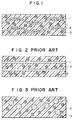
- Fig. 1 illustrates the construction of a laminate according to the present invention.
- the laminate can be fabricated by stacking and bonding two pieces of prepreg each of which is obtained in such a way that a woven reinforcement 1 is impregnated with a resin portion 2 having a sea-island structure and is then dried.
- the woven reinforcement 1 exists entirely in the planar direction of the laminate. Therefore, the effect of reducing the thermal expansion coefficient of the laminate in the planar direction thereof can be utilized to the utmost on the basis of the sea-island structure.
- numeral 3 in Fig. 1 designates a dispersed (island) phase.
- the laminate Since an organic resin matrix constituting the resin portion 2 of the sea-island structure is continuously existent penetrating the reinforcement members 1, the laminate is free from the problem of bonding at the interface between different phases in a composite material.
- Fig. 2 illustrates the construction of a laminate in the prior art.
- the construction is very effective in reducing the thermal expansion coefficient of the laminate in the planar direction thereof.
- a resin matrix which constitutes a resin portion 2 of sea-island structure including islands 3 does not continuously penetrate reinforcement members 1. Therefore, the laminate is liable to pose the problem of bonding at the interface between different phases, and so forth.
- Fig. 3 illustrates the construction of a laminate in the prior art.
- a woven reinforcement 1 exists in the form of independent particles, so that the whole laminate exhibits an isotropy. It is therefore impossible to make the most of the effect of reducing the thermal expansion coefficient of the laminate, in the planar direction thereof.
- the effect is based on the interaction between a resin matrix and islands 3 which form a resin portion 2 of sea-island structure.
- Pieces of E-glass (electrical glass) cloth each being 100 [ ⁇ m] thick were respectively impregnated and coated with the varnish samples, and then dried at 120 [°C] for 10 [min] so as to remove the solvent. Thus, pieces of prepreg were obtained.
- the resin content of each of the obtained prepreg pieces was 70 [weight-%].
- Copper foils (each being 18 [ ⁇ m] thick) were respectively superposed on both the surfaces of each of the obtained prepreg pieces, and the resulting structures were respectively pressed under heat by a press. Thus, laminates were obtained.
- two-stage reactions at 130 [°C] for 30 [min] and at 180 [°C] for 60 [min] were performed, and a pressure of 196.2 N/cm2 (20 [kg/cm2])was held.
- the copper foil peeling strengths of the obtained laminates, and the thermal expansion coefficients of the laminates in the planar directions thereof after having etched the copper foils were respectively evaluated by the TMA (Thermal Mechanical Analyzer) method.
- Resin components were prescribed in such a way that 55 parts [by weight] of phenol novolac (trade name "H100", produced by Hitachi Chamical Co., Ltd.) as a setting agent and 15 parts [by weight] of carboxyl-group-terminal perfluoroether type compound (produced by Mitsui Fluorochemical Kabushiki-Kaisha) as a component of low elastic modulus were added to 100 parts [by weight] of epoxy compound ("YX4000H", Yuka Shell Kabushiki-Kaisha).
- phenol novolac trade name "H100", produced by Hitachi Chamical Co., Ltd.
- carboxyl-group-terminal perfluoroether type compound produced by Mitsui Fluorochemical Kabushiki-Kaisha
- a laminate and a resin sheet were fabricated from the obtained prepreg by the same methods as in Examples 6 ⁇ 8, and their characteristics were similarly estimated.
- Examples 1 thru 4 and Comparative Examples 1 and 2 packaged articles were fabricated for Examples 6 thru 9, and the samples thereof were tested as to the defects of soldered connection parts.
- Example 6 thru 9 The measured characteristics of Examples 6 thru 9 are listed in Table 2 below: TABLE 2 Coeff. of In-plane thermal expansion [ ⁇ 106/K] Elastic modulus (kg ⁇ f/mm2) Glass transition temperature [°C] Number of Defective parts (in 100 parts) Example 6 8.7 297 188 0 Example 7 8.5 290 195 0 Example 8 7.6 280 197 0 Example 9 8.0 282 202 0
- the coefficients of thermal expansion of a laminate, a multilayer printed circuit board and a prepreg in the planar directions thereof are reduced along with the elastic moduli thereof, thereby making it possible to remarkably lower thermal stresses which arise on packaging surfaces and to sharply enhance the reliabilities of the connections of the laminate etc. with articles or elements which are to be packaged.
Landscapes
- Chemical & Material Sciences (AREA)
- Engineering & Computer Science (AREA)
- Materials Engineering (AREA)
- Manufacturing & Machinery (AREA)
- Health & Medical Sciences (AREA)
- Chemical Kinetics & Catalysis (AREA)
- Medicinal Chemistry (AREA)
- Polymers & Plastics (AREA)
- Organic Chemistry (AREA)
- Inorganic Chemistry (AREA)
- Textile Engineering (AREA)
- Microelectronics & Electronic Packaging (AREA)
- Laminated Bodies (AREA)
- Production Of Multi-Layered Print Wiring Board (AREA)
- Reinforced Plastic Materials (AREA)
Applications Claiming Priority (2)
| Application Number | Priority Date | Filing Date | Title |
|---|---|---|---|
| JP22844593A JP3648750B2 (ja) | 1993-09-14 | 1993-09-14 | 積層板及び多層プリント回路板 |
| JP228445/93 | 1993-09-14 |
Publications (2)
| Publication Number | Publication Date |
|---|---|
| EP0642919A1 true EP0642919A1 (fr) | 1995-03-15 |
| EP0642919B1 EP0642919B1 (fr) | 1997-10-22 |
Family
ID=16876609
Family Applications (1)
| Application Number | Title | Priority Date | Filing Date |
|---|---|---|---|
| EP94110617A Expired - Lifetime EP0642919B1 (fr) | 1993-09-14 | 1994-07-07 | Produit laminé et plaque de circuit imprimé multicouche |
Country Status (3)
| Country | Link |
|---|---|
| EP (1) | EP0642919B1 (fr) |
| JP (1) | JP3648750B2 (fr) |
| DE (1) | DE69406390T2 (fr) |
Cited By (6)
| Publication number | Priority date | Publication date | Assignee | Title |
|---|---|---|---|---|
| DE19635282A1 (de) * | 1995-09-07 | 1997-03-13 | Hitachi Chemical Co Ltd | Verfahren zur Herstellung eines Metallplattierungslaminats |
| EP0907204A3 (fr) * | 1997-10-03 | 1999-08-18 | Nec Corporation | Dispositif semiconducteur ayant la taille d'une puce et son procédé de fabrication |
| EP1073320A3 (fr) * | 1999-07-29 | 2004-01-02 | Mitsubishi Gas Chemical Company, Inc. | Matériau de base d'un tissu de verre et résine thermodurcissable comme laminé revêtu de cuivre ayant une haute élasticité |
| EP0959500A3 (fr) * | 1998-05-19 | 2004-09-29 | Lucent Technologies Inc. | Empaquetage de modules à multi-puces de type silicium-sur-silicium |
| US8322201B2 (en) | 2008-01-09 | 2012-12-04 | Dow Global Technologies Llc | Device and method for assessing the machinability of laminates |
| EP2639822A2 (fr) * | 2012-03-13 | 2013-09-18 | Shin-Etsu Chemical Co., Ltd. | Procédé de fabrication par moulage en résine d'un dispositif semi-conducteur |
Families Citing this family (10)
| Publication number | Priority date | Publication date | Assignee | Title |
|---|---|---|---|---|
| US6207595B1 (en) | 1998-03-02 | 2001-03-27 | International Business Machines Corporation | Laminate and method of manufacture thereof |
| JP2005243830A (ja) * | 2004-02-25 | 2005-09-08 | Kyocera Chemical Corp | プリント配線板 |
| US7078816B2 (en) | 2004-03-31 | 2006-07-18 | Endicott Interconnect Technologies, Inc. | Circuitized substrate |
| US7145221B2 (en) | 2004-03-31 | 2006-12-05 | Endicott Interconnect Technologies, Inc. | Low moisture absorptive circuitized substrate, method of making same, electrical assembly utilizing same, and information handling system utilizing same |
| US7270845B2 (en) | 2004-03-31 | 2007-09-18 | Endicott Interconnect Technologies, Inc. | Dielectric composition for forming dielectric layer for use in circuitized substrates |
| JP2006312751A (ja) * | 2006-08-10 | 2006-11-16 | Sumitomo Bakelite Co Ltd | 樹脂組成物、プリプレグ及びそれを用いた銅張積層板 |
| JP5361589B2 (ja) * | 2009-07-21 | 2013-12-04 | ユニチカ株式会社 | 離型シート |
| JP2012079765A (ja) * | 2010-09-30 | 2012-04-19 | Fdk Corp | 電子部品実装基板 |
| JP6255668B2 (ja) * | 2011-01-18 | 2018-01-10 | 日立化成株式会社 | プリプレグ及びこれを用いた積層板並びにプリント配線板 |
| JP2014111719A (ja) * | 2012-11-12 | 2014-06-19 | Panasonic Corp | 積層板、金属張積層板、プリント配線板、多層プリント配線板 |
Citations (4)
| Publication number | Priority date | Publication date | Assignee | Title |
|---|---|---|---|---|
| JPH02219853A (ja) * | 1989-02-21 | 1990-09-03 | Matsushita Electric Works Ltd | 配線板用樹脂組成物およびプリプレグ |
| EP0412827A2 (fr) * | 1989-08-09 | 1991-02-13 | Imperial Chemical Industries Plc | Composition de polymère |
| EP0559437A1 (fr) * | 1992-03-02 | 1993-09-08 | Toray Industries, Inc. | Tissu préimpregné et son procédé de production |
| EP0581314A2 (fr) * | 1992-07-31 | 1994-02-02 | International Business Machines Corporation | Résines de dicyanate ester modifié ayant une ténacité élevée à la rupture |
Family Cites Families (3)
| Publication number | Priority date | Publication date | Assignee | Title |
|---|---|---|---|---|
| JP2913886B2 (ja) * | 1991-04-24 | 1999-06-28 | 松下電工株式会社 | プリント配線板 |
| JP2898809B2 (ja) * | 1991-12-13 | 1999-06-02 | 住友ベークライト株式会社 | 積層板の製造方法 |
| JP3047593B2 (ja) * | 1992-02-13 | 2000-05-29 | 日立化成工業株式会社 | 印刷配線板用プリプレグの製造方法及びそれを用いた金属芯入り銅張積層板 |
-
1993
- 1993-09-14 JP JP22844593A patent/JP3648750B2/ja not_active Expired - Fee Related
-
1994
- 1994-07-07 DE DE69406390T patent/DE69406390T2/de not_active Expired - Lifetime
- 1994-07-07 EP EP94110617A patent/EP0642919B1/fr not_active Expired - Lifetime
Patent Citations (4)
| Publication number | Priority date | Publication date | Assignee | Title |
|---|---|---|---|---|
| JPH02219853A (ja) * | 1989-02-21 | 1990-09-03 | Matsushita Electric Works Ltd | 配線板用樹脂組成物およびプリプレグ |
| EP0412827A2 (fr) * | 1989-08-09 | 1991-02-13 | Imperial Chemical Industries Plc | Composition de polymère |
| EP0559437A1 (fr) * | 1992-03-02 | 1993-09-08 | Toray Industries, Inc. | Tissu préimpregné et son procédé de production |
| EP0581314A2 (fr) * | 1992-07-31 | 1994-02-02 | International Business Machines Corporation | Résines de dicyanate ester modifié ayant une ténacité élevée à la rupture |
Non-Patent Citations (1)
| Title |
|---|
| DATABASE WPI Week 9041, Derwent World Patents Index; AN 90-309588 * |
Cited By (8)
| Publication number | Priority date | Publication date | Assignee | Title |
|---|---|---|---|---|
| DE19635282A1 (de) * | 1995-09-07 | 1997-03-13 | Hitachi Chemical Co Ltd | Verfahren zur Herstellung eines Metallplattierungslaminats |
| DE19635282C2 (de) * | 1995-09-07 | 2002-10-31 | Hitachi Chemical Co Ltd | Verfahren zur Herstellung eines Metallplattierungslaminats |
| EP0907204A3 (fr) * | 1997-10-03 | 1999-08-18 | Nec Corporation | Dispositif semiconducteur ayant la taille d'une puce et son procédé de fabrication |
| EP0959500A3 (fr) * | 1998-05-19 | 2004-09-29 | Lucent Technologies Inc. | Empaquetage de modules à multi-puces de type silicium-sur-silicium |
| EP1073320A3 (fr) * | 1999-07-29 | 2004-01-02 | Mitsubishi Gas Chemical Company, Inc. | Matériau de base d'un tissu de verre et résine thermodurcissable comme laminé revêtu de cuivre ayant une haute élasticité |
| US8377544B2 (en) | 1999-07-29 | 2013-02-19 | Mitsubishi Gas Chemical Company, Inc. | Glass fabric base material/thermosetting resin copper-clad laminate having a high-elasticity |
| US8322201B2 (en) | 2008-01-09 | 2012-12-04 | Dow Global Technologies Llc | Device and method for assessing the machinability of laminates |
| EP2639822A2 (fr) * | 2012-03-13 | 2013-09-18 | Shin-Etsu Chemical Co., Ltd. | Procédé de fabrication par moulage en résine d'un dispositif semi-conducteur |
Also Published As
| Publication number | Publication date |
|---|---|
| JP3648750B2 (ja) | 2005-05-18 |
| DE69406390T2 (de) | 1998-05-20 |
| DE69406390D1 (de) | 1997-11-27 |
| JPH0786710A (ja) | 1995-03-31 |
| EP0642919B1 (fr) | 1997-10-22 |
Similar Documents
| Publication | Publication Date | Title |
|---|---|---|
| US5677045A (en) | Laminate and multilayer printed circuit board | |
| EP0642919B1 (fr) | Produit laminé et plaque de circuit imprimé multicouche | |
| US5103293A (en) | Electronic circuit packages with tear resistant organic cores | |
| US6849934B2 (en) | Dielectric film for printed wiring board, multilayer printed board, and semiconductor device | |
| US9236169B2 (en) | Electromagnetic wave shielding structure and method for fabricating the same | |
| EP2180772A1 (fr) | Tableau de connexions à couches multiples et dispositif à semi-conducteur | |
| KR100602537B1 (ko) | 반도체 접속 기판용 접착제 부착 테이프 및 그것을 사용한동박 적층판 | |
| US6489013B2 (en) | Resin compound, and adhesive film, metal-clad adhesive film, circuit board, and assembly structure, using the resin compound | |
| US20050269128A1 (en) | Semiconductor module with high process accuracy, manufacturing method thereof, and semiconductor device therewith | |
| KR101574907B1 (ko) | 프리프레그, 적층판, 반도체 패키지 및 적층판의 제조 방법 | |
| US6534181B2 (en) | Styrene-maleic anhydride copolymer and epoxy resin blend crosslinked with multifunctional amine compounds | |
| JP4269746B2 (ja) | プリント配線板の製造方法、プリント配線板および半導体パッケージ | |
| US5166037A (en) | Method of additive circuitization of circuit boards with high adhesion, voidless copper leads | |
| JP3838250B2 (ja) | 積層板及び多層プリント回路板 | |
| JPH10321974A (ja) | 回路形成用基板 | |
| US5176811A (en) | Gold plating bath additives for copper circuitization on polyimide printed circuit boards | |
| WO2007108087A1 (fr) | Couche de résine isolante, couche de résine isolante sur un support et carte à circuit imprimé multicouche | |
| JPH07224269A (ja) | 接着剤組成物及び複合体、プリント配線板 | |
| US5250347A (en) | Mechanically enhanced, high impact strength triazine resins, and method of preparing same | |
| JP5696302B2 (ja) | インターポーザ用の金属張積層板とそれを用いた半導体パッケージ | |
| US7931830B2 (en) | Dielectric composition for use in circuitized substrates and circuitized substrate including same | |
| JP2007129215A (ja) | 回路基板において使用される絶縁組成物、およびこの絶縁組成物を使用して形成した回路基板 | |
| Korleski et al. | New composite organic dielectric for high performance flip chip single chip packages | |
| Kikuchi et al. | Maleimide Resin Blends with Enhanced Toughness for High-Temperature Semiconductor Packaging | |
| JPH1135659A (ja) | 樹脂組成物、プリプレグおよびプリント配線基板とその製造方法 |
Legal Events
| Date | Code | Title | Description |
|---|---|---|---|
| PUAI | Public reference made under article 153(3) epc to a published international application that has entered the european phase |
Free format text: ORIGINAL CODE: 0009012 |
|
| 17P | Request for examination filed |
Effective date: 19950109 |
|
| AK | Designated contracting states |
Kind code of ref document: A1 Designated state(s): DE FR GB |
|
| 17Q | First examination report despatched |
Effective date: 19950420 |
|
| GRAG | Despatch of communication of intention to grant |
Free format text: ORIGINAL CODE: EPIDOS AGRA |
|
| GRAH | Despatch of communication of intention to grant a patent |
Free format text: ORIGINAL CODE: EPIDOS IGRA |
|
| GRAH | Despatch of communication of intention to grant a patent |
Free format text: ORIGINAL CODE: EPIDOS IGRA |
|
| GRAA | (expected) grant |
Free format text: ORIGINAL CODE: 0009210 |
|
| AK | Designated contracting states |
Kind code of ref document: B1 Designated state(s): DE FR GB |
|
| REF | Corresponds to: |
Ref document number: 69406390 Country of ref document: DE Date of ref document: 19971127 |
|
| ET | Fr: translation filed | ||
| PLBE | No opposition filed within time limit |
Free format text: ORIGINAL CODE: 0009261 |
|
| STAA | Information on the status of an ep patent application or granted ep patent |
Free format text: STATUS: NO OPPOSITION FILED WITHIN TIME LIMIT |
|
| 26N | No opposition filed | ||
| REG | Reference to a national code |
Ref country code: GB Ref legal event code: IF02 |
|
| PGFP | Annual fee paid to national office [announced via postgrant information from national office to epo] |
Ref country code: FR Payment date: 20110727 Year of fee payment: 18 |
|
| PGFP | Annual fee paid to national office [announced via postgrant information from national office to epo] |
Ref country code: GB Payment date: 20110706 Year of fee payment: 18 Ref country code: DE Payment date: 20110629 Year of fee payment: 18 |
|
| GBPC | Gb: european patent ceased through non-payment of renewal fee |
Effective date: 20120707 |
|
| REG | Reference to a national code |
Ref country code: FR Ref legal event code: ST Effective date: 20130329 |
|
| PG25 | Lapsed in a contracting state [announced via postgrant information from national office to epo] |
Ref country code: FR Free format text: LAPSE BECAUSE OF NON-PAYMENT OF DUE FEES Effective date: 20120731 Ref country code: DE Free format text: LAPSE BECAUSE OF NON-PAYMENT OF DUE FEES Effective date: 20130201 Ref country code: GB Free format text: LAPSE BECAUSE OF NON-PAYMENT OF DUE FEES Effective date: 20120707 |
|
| REG | Reference to a national code |
Ref country code: DE Ref legal event code: R119 Ref document number: 69406390 Country of ref document: DE Effective date: 20130201 |