EP0644521A2 - Speicherung und Auslesen von Daten unter Verwendung der residuellen Kapazität des Rasterpufferspeichers - Google Patents
Speicherung und Auslesen von Daten unter Verwendung der residuellen Kapazität des Rasterpufferspeichers Download PDFInfo
- Publication number
- EP0644521A2 EP0644521A2 EP94306816A EP94306816A EP0644521A2 EP 0644521 A2 EP0644521 A2 EP 0644521A2 EP 94306816 A EP94306816 A EP 94306816A EP 94306816 A EP94306816 A EP 94306816A EP 0644521 A2 EP0644521 A2 EP 0644521A2
- Authority
- EP
- European Patent Office
- Prior art keywords
- frame buffer
- address space
- data
- residual
- clipping
- Prior art date
- Legal status (The legal status is an assumption and is not a legal conclusion. Google has not performed a legal analysis and makes no representation as to the accuracy of the status listed.)
- Withdrawn
Links
- 239000000872 buffer Substances 0.000 title claims abstract description 104
- 238000000034 method Methods 0.000 claims abstract description 13
- 238000013500 data storage Methods 0.000 claims description 5
- 238000000638 solvent extraction Methods 0.000 claims description 4
- 238000009877 rendering Methods 0.000 abstract description 16
- 238000006243 chemical reaction Methods 0.000 abstract description 14
- 230000000873 masking effect Effects 0.000 abstract description 12
- 238000010586 diagram Methods 0.000 description 3
- 230000006870 function Effects 0.000 description 2
- 230000008520 organization Effects 0.000 description 2
- 239000007853 buffer solution Substances 0.000 description 1
- 230000003139 buffering effect Effects 0.000 description 1
- 230000008859 change Effects 0.000 description 1
- 239000002131 composite material Substances 0.000 description 1
- 238000013506 data mapping Methods 0.000 description 1
- 230000007423 decrease Effects 0.000 description 1
- 230000000694 effects Effects 0.000 description 1
- 230000008569 process Effects 0.000 description 1
Images

Classifications
-
- G—PHYSICS
- G09—EDUCATION; CRYPTOGRAPHY; DISPLAY; ADVERTISING; SEALS
- G09G—ARRANGEMENTS OR CIRCUITS FOR CONTROL OF INDICATING DEVICES USING STATIC MEANS TO PRESENT VARIABLE INFORMATION
- G09G5/00—Control arrangements or circuits for visual indicators common to cathode-ray tube indicators and other visual indicators
- G09G5/36—Control arrangements or circuits for visual indicators common to cathode-ray tube indicators and other visual indicators characterised by the display of a graphic pattern, e.g. using an all-points-addressable [APA] memory
- G09G5/39—Control of the bit-mapped memory
- G09G5/393—Arrangements for updating the contents of the bit-mapped memory
Definitions
- the present invention generally relates to the storage and retrieval of data during the computer generation of graphics images on a video display screen. More particularly, the invention is directed to a system and method for efficiently generating, storing and retrieving clipping, masking or stenciling plane data used in conjunction with video display images rendered into a frame buffer.
- the rendering, storage and eventual display of graphics images defined by computer systems is an area of technology undergoing much competition and evolution.
- Presently preferred systems used to generate high resolution and color range graphics images use high speed raster engines to convert primitives defined by central processors into color images stored as binary data in a video frequency random access memory known as a frame buffer.
- the data in the frame buffer is stored in a raster format corresponding to the video display, with the depth of the frame buffer, defined by bit planes, corresponding to the color resolution.
- the frame buffer is scanned in synchronism with the video display screen to generate the final image.
- High performance work stations also typically include additional bit planes, corresponding in size to the frame buffer, for storing windows data and data for other general masking or clipping applications.
- Configurations of VRAM chips normally create frame buffers having fixed addressable ranges incremented in powers of 2, while video display screens are not so proportioned. Therefore, unused or residual portions of frame buffer memory typically remain.
- the typical frame buffer is 1024x1024 in size. Therefore, the frame buffer contains an unused or residual addressable memory space of 1024x256.
- the depth of the residual memory corresponds to the number of the bit planes in the used portion of the frame buffer.
- the frame buffer is composed of 8 bit planes.
- 24 bits of data, 8 each of RGB, are used to represent each pixel in the frame buffer.
- the invention provides a data storage system for graphics data, including: a multiple bit plane frame buffer having address space for storing data to be displayed and having residual address space; means for partitioning the displayable frame buffer address space into two or more portions; means for relating displayable frame buffer address space in the two or more portions to particular bit planes of the residual address space; and means for locating clipping frame data by frame buffer portions in respective related bit planes of the residual address space.
- the invention provides a method for storing clipping plane data in the residual address space of a multiple bit plane frame buffer having adddress space for storing data to be displayed and residual address space, comprising the steps of; partitioning displayable frame buffer address space into two or more portions; relating displayable frame buffer address space in the two or more portions to particular bit planes of the residual address space; and locating clipping plane data by frame buffer portion in respective related bit planes of the residual address space.
- the system and method of the present invention efficiently utilizes residual frame buffer memory to render, store and access clipping, masking, stenciling, windowing, overlay, underlay, and the like data, hereinafter generally referred to as clipping data, on a per pixel basis with minimum complexity and at a speed consistent with the rendering rate of the graphics display system.
- clipping data corresponding by pixel to the screen image rendered into the frame buffer is stored in a succession of bit planes within the residual memory of the frame buffer.
- the relative size of the residual frame buffer memory to the full frame buffer memory defines the number of bit planes needed for storing the clipping planes.
- the invention as preferably embodied involves a multiple bit plane frame buffer which is larger in size than the video display which it supports.
- the unused or residual memory of the frame buffer is used to store clipping plane data in an arrangement which divides the displayed section of the frame buffer into portions, and folds or stacks the corresponding clipping plane data into the residual section of the frame buffer by relating frame buffer bit planes to the aforementioned portions of the addressed frame buffer.
- Rendering of the clipping data into the residual portion of the frame buffer is readily accomplished using frame buffer plane masking.
- Clipping data is applied to rendered images in relatively conventional manner.
- the address shifting needed to align clipping data by pixels to corresponding displayed frame buffer portion pixels is accomplished with relatively few comparison and addition circuits. Thereby, expensive VRAM frame buffer memory is efficiently utilized while maintaining system speed and without unduly complicating the rendering into the display portion of the frame buffer.
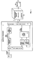
- Figure 1 illustrates by blocked diagram the key elements within the context of which the present invention is practiced. These include central processing unit 1, which defines the graphics primitives to be generated, graphics processor 2, used to render the individual pixels which make up the graphics image, frame buffer memory 3, storing the image to be displayed, and display 4, depicting the image in a form perceivable by a human user.
- the rasterization means used to convert multiple bit planes of data stored in the frame buffer into color images on the display is omitted in that it is well known and therefore does not contribute meaningfully to the understanding of the invention.
- display 4 is not square in pixel distribution, but, rather, represents a conventional rectangular graphic display screen of 1024x768 pixels.
- Frame buffer 3 uses conventional VRAM type memory devices and consequently needs an x-y direction address space of 1024x1024 to support 1024x768 display 4.
- Moderately priced graphics systems will typically have frame buffers with 8 bit planes, providing 8 bits per pixel position color resolution. It should be understood that the frame buffer can have greater or fewer bit planes, with fewer providing relatively meager color resolution while larger numbers, typically 24, provide near ideal color resolution. In like manner, the architecture of the overall system can use multiple frame buffers when the need arises, allowing one to be modified as the other is being scanned for display.
- the invention focuses on the effective and efficient utilization of the unused or residual portion 6 of frame buffer 3 to store data which can be used for clipping, masking or stenciling purposes during the rendering of the images into the displayed portion of the frame buffer.
- additional bit planes could be added to the frame buffer to store this data.
- these additional planes are relatively expensive VRAM memory, a part of which again is unused or residual. Therefore, the basic structure and organization of the frame buffer remains unchanged.
- Graphics processor 2 as detailed at 2 in Figure 1 is relatively conventional in organization and operation. Graphics processor 2 is shown to include bus interface 7 at one side and frame buffer memory interface 8 at the opposite side. Rendering engine 9 remains relatively normal, but is connected through clip address generator 11 to memory interface 8. In the present embodiment, clip address generator 11 provides the address conversion needed to properly locate the clipping plane data portion 6 of frame buffer 3.
- Graphics processor 2 also includes rendering data register 12, clipping data register 13, and clip compare logic 14, which together function in relatively conventional manner to mask or clip newly generated pixel data based upon the state of the corresponding pixel within the mask stored in residual portion 6 of frame buffer 3.
- the invention focuses on the effective use of this fundamental architecture to render, store and use clipping data.
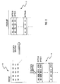
- FIG. 2 depicts and contrasts the storage of clipping data in the residual portion of the frame buffer as practiced through software manipulation in the prior art and as presently disclosed.
- Display referenced pixel positions are shown generally at 16, extending in a X-Y format across the screen.
- Storage of clipping data in unused or residual portions of the frame buffer according to the prior art is shown generally at 17, where the clip data for pixel positions AO, BO, CO and DO, are stacked in the successive 8 bit planes of each residual frame buffer address. Data for successive positions is then stacked in the planes of successive frame buffer addresses.
- the conversion of the clipping data addresses was slow, usually requiring software manipulation of the address information.
- the present system and method of storing clipping data creates the arrangement depicted generally at 18.
- a conceptual depiction of the address conversion this folded type storage of clipping data appears in Figure 3, the figure further depicts the earlier shown use of 1024x1024 pixel by 8 bit plane frame buffer 3 in association with a 1024x768 display.
- the residual memory is composed of 8 bit planes of 1024 by 256 dimension.
- the clipping data is stored in the first 6 bit planes of residual frame buffer memory 6.
- the address conversion is accomplished in the manner conceptually depicted in Figure 3.
- the displayed part of the frame buffer is divided into three portions, consistent with the 256 size of the residual memory.
- Two planes of clipping data 19, which are related to the pixels in upper portion 21 of frame buffer 3, are stored in the first two planes of residual frame buffer memory 6.
- the successive two planes of clipping data 22, which are associated with the pixels in portion 24 of the frame buffer, define the next two planes in the residual portion of the frame buffer.
- a similar address conversion relationship is established between the two planes of clipping data 26 and portion 27 of the pixel related frame buffer. As embodied, the last two planes of residual frame buffer 6 are unused.
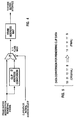
- Figure 4 schematically illustrates the operations which are performed within clip address generator 11 ( Figure 1).
- the rendering engine provides x-y pixel data and plane masked data.
- the normal address mode is selected and the addresses pass through gate 28 to the conventional VRAM address map.
- gate 28 is switched so that the converted address output from clip address conversion block 29 is provided to the VRAM address map circuitry.
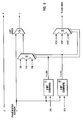
- Figure 6 provides a schematic of devices suitable to accomplish the clipping address conversion described with reference to Figure 4, and the plane masking described with reference to Figure 5. Note that the X direction address is not converted.
- 2 bit comparators 31 and 32 determine whether the pixel being addressed is situated within portions 21, 24 or 27 ( Figure 3) of the frame buffer. Depending on the outcome, gate 33 increments the frame buffer Y address to position the data within the appropriate relative pixel position as exists within residual frame buffer memory 6.
- Two bit adder 34 accomplishes this operation by incrementing the most significate bits of the Y address.
- the frame buffer bit plane masking information is generated in gate 36, and is likewise responsive to the outputs of comparators 31 and 32. During the rendering of clipping data into the residual portion of the frame buffer, gate 36 determines which of the frame buffer planes is to be masked in direct correspondence to the portion of the frame buffer to which the clipping data pertains.
- the clipping plane storage system and method of the present invention utilizes residual frame buffer memory so that address translation can be accomplished with high speed hardware for both the storing and the reading of the clipping plane data.
- a double buffered frame buffer system doubles the number of the planes available for storing clipping data.
- a double buffer version of frame buffer 3 as depicted in Figure 3 would provide 16 bit planes for clipping data.
- the preferred implementation for such a system involves the use of 4 clip planes folded into the first 12 of the 16 bit planes within the residual portion of the frame buffer. Though from a data storage perspective the 16 bit planes in the residual portion of the frame buffer have adequate memory to hold 5 clipping planes, the address translation associated with using the 5th plane would unacceptably reduce the conversion speed.
- a 24 bit plane graphics display system provides storage capability for 8 clipping, masking or stenciling patterns.
Landscapes
- Engineering & Computer Science (AREA)
- Physics & Mathematics (AREA)
- Computer Hardware Design (AREA)
- General Physics & Mathematics (AREA)
- Theoretical Computer Science (AREA)
- Image Generation (AREA)
- Controls And Circuits For Display Device (AREA)
- Digital Computer Display Output (AREA)
- Image Input (AREA)
- Memory System (AREA)
Applications Claiming Priority (2)
| Application Number | Priority Date | Filing Date | Title |
|---|---|---|---|
| US12382393A | 1993-09-20 | 1993-09-20 | |
| US123823 | 1993-09-20 |
Publications (1)
| Publication Number | Publication Date |
|---|---|
| EP0644521A2 true EP0644521A2 (de) | 1995-03-22 |
Family
ID=22411107
Family Applications (1)
| Application Number | Title | Priority Date | Filing Date |
|---|---|---|---|
| EP94306816A Withdrawn EP0644521A2 (de) | 1993-09-20 | 1994-09-19 | Speicherung und Auslesen von Daten unter Verwendung der residuellen Kapazität des Rasterpufferspeichers |
Country Status (3)
| Country | Link |
|---|---|
| US (1) | US5668979A (de) |
| EP (1) | EP0644521A2 (de) |
| JP (1) | JP2647348B2 (de) |
Families Citing this family (3)
| Publication number | Priority date | Publication date | Assignee | Title |
|---|---|---|---|---|
| US6359630B1 (en) * | 1999-06-14 | 2002-03-19 | Sun Microsystems, Inc. | Graphics system using clip bits to decide acceptance, rejection, clipping |
| JP2008299642A (ja) * | 2007-05-31 | 2008-12-11 | Mitsubishi Electric Corp | 図形描画装置 |
| WO2013097069A1 (en) * | 2011-12-26 | 2013-07-04 | Intel Corporation | Multiple scissor plane registers for rendering image data |
Family Cites Families (17)
| Publication number | Priority date | Publication date | Assignee | Title |
|---|---|---|---|---|
| JPS60217385A (ja) * | 1984-04-13 | 1985-10-30 | 株式会社日立製作所 | 画像表示方式 |
| US4646078A (en) * | 1984-09-06 | 1987-02-24 | Tektronix, Inc. | Graphics display rapid pattern fill using undisplayed frame buffer memory |
| JPH0774946B2 (ja) * | 1985-05-20 | 1995-08-09 | 株式会社日立製作所 | 記憶回路 |
| US4745407A (en) * | 1985-10-30 | 1988-05-17 | Sun Microsystems, Inc. | Memory organization apparatus and method |
| JPS62231380A (ja) * | 1986-03-31 | 1987-10-09 | Namuko:Kk | 画像合成装置 |
| US4903217A (en) * | 1987-02-12 | 1990-02-20 | International Business Machines Corp. | Frame buffer architecture capable of accessing a pixel aligned M by N array of pixels on the screen of an attached monitor |
| GB2203316B (en) * | 1987-04-02 | 1991-04-03 | Ibm | Display system with symbol font memory |
| US5061919A (en) * | 1987-06-29 | 1991-10-29 | Evans & Sutherland Computer Corp. | Computer graphics dynamic control system |
| CA1317041C (en) * | 1987-12-24 | 1993-04-27 | Ncr Corporation | Apparatus for creating a cursor pattern by strips related to individual scan lines |
| JPH01263778A (ja) * | 1988-04-14 | 1989-10-20 | Sanyo Electric Co Ltd | 画像メモリのアドレス制御方法 |
| JPH0281088A (ja) * | 1988-09-19 | 1990-03-22 | Hitachi Ltd | 表示装置 |
| JPH0281087A (ja) * | 1988-09-19 | 1990-03-22 | Seiko Epson Corp | 表示制御装置 |
| JP2796329B2 (ja) * | 1989-02-08 | 1998-09-10 | 株式会社日立製作所 | 表示メモリとそれを備えた画像処理装置 |
| JPH03185492A (ja) * | 1989-12-14 | 1991-08-13 | Matsushita Electric Ind Co Ltd | 画像メモリの割当て方法、及びアドレス生成回路 |
| US5007001A (en) * | 1990-01-24 | 1991-04-09 | Lloyd Williams Andrew | Method for reordering the pixel map of a digitized image |
| EP0448287B1 (de) * | 1990-03-16 | 1996-09-18 | Hewlett-Packard Company | Verfahren und Einrichtung zum Abschneiden von Pixeln von Quellen- und Zielfenstern in einem graphischen System |
| US5252953A (en) * | 1990-05-22 | 1993-10-12 | American Film Technologies, Inc. | Computergraphic animation system |
-
1994
- 1994-08-26 JP JP6202549A patent/JP2647348B2/ja not_active Expired - Lifetime
- 1994-09-19 EP EP94306816A patent/EP0644521A2/de not_active Withdrawn
-
1995
- 1995-01-06 US US08/369,577 patent/US5668979A/en not_active Expired - Fee Related
Also Published As
| Publication number | Publication date |
|---|---|
| US5668979A (en) | 1997-09-16 |
| JPH07152637A (ja) | 1995-06-16 |
| JP2647348B2 (ja) | 1997-08-27 |
Similar Documents
| Publication | Publication Date | Title |
|---|---|---|
| US6765581B2 (en) | Display apparatus and method capable of rotating an image by 180 degrees | |
| JP3286331B2 (ja) | ブロックテクスチャコンプレックスクリップマスクプロセッサ | |
| US4330834A (en) | Graphics display apparatus | |
| US5606650A (en) | Method and apparatus for storage and retrieval of a texture map in a graphics display system | |
| US4648045A (en) | High speed memory and processor system for raster display | |
| US5956049A (en) | Hardware that rotates an image for portrait-oriented display | |
| US3973245A (en) | Method and apparatus for point plotting of graphical data from a coded source into a buffer and for rearranging that data for supply to a raster responsive device | |
| GB2104354A (en) | Writing text characters on computer graphics display | |
| US6133923A (en) | Method and apparatus for texture data | |
| US4566000A (en) | Image display apparatus and method having virtual cursor | |
| JPS6049391A (ja) | ラスタ走査表示システム | |
| US6943797B2 (en) | Early primitive assembly and screen-space culling for multiple chip graphics system | |
| JPH05244402A (ja) | 必要な記憶装置の量を低減する方法 | |
| US20020149594A1 (en) | Video graphic interface device and method for portrait and landscape image display modes | |
| US4918429A (en) | Display system with symbol font memory | |
| EP0519694A2 (de) | Verfahren zur Zuteilung von Speicherplätzen ausserhalb des Bildschirms | |
| US5668979A (en) | Storage of clipping plane data in successive bit planes of residual frame buffer memory | |
| US20030231176A1 (en) | Memory access device, semiconductor device, memory access method, computer program and recording medium | |
| EP0593012B1 (de) | Videobilderanzeigevorrichtung und Verfahren zum Steuern einer Videobilderanzeige | |
| JPS58211186A (ja) | 分割画面表示制御方式 | |
| GB2226478A (en) | Converting rectilinear (x,y) information into pixel position for a raster scan display of plural horizontal resolutions | |
| US5093905A (en) | Inclined rectangular pattern generating system | |
| EP0744730A2 (de) | Anzeigeeinrichtung mit Zeichenmaskierungsfunktion | |
| Rost | Using OpenGL for imaging | |
| JP4195953B2 (ja) | 画像処理装置 |
Legal Events
| Date | Code | Title | Description |
|---|---|---|---|
| PUAI | Public reference made under article 153(3) epc to a published international application that has entered the european phase |
Free format text: ORIGINAL CODE: 0009012 |
|
| AK | Designated contracting states |
Kind code of ref document: A2 Designated state(s): DE FR GB |
|
| 17P | Request for examination filed |
Effective date: 19950714 |
|
| STAA | Information on the status of an ep patent application or granted ep patent |
Free format text: STATUS: THE APPLICATION HAS BEEN WITHDRAWN |
|
| 18W | Application withdrawn |
Withdrawal date: 19960730 |