EP0646871A2 - Système à gérer le transfert de données - Google Patents
Système à gérer le transfert de données Download PDFInfo
- Publication number
- EP0646871A2 EP0646871A2 EP94307121A EP94307121A EP0646871A2 EP 0646871 A2 EP0646871 A2 EP 0646871A2 EP 94307121 A EP94307121 A EP 94307121A EP 94307121 A EP94307121 A EP 94307121A EP 0646871 A2 EP0646871 A2 EP 0646871A2
- Authority
- EP
- European Patent Office
- Prior art keywords
- data
- transfer
- temporarily holding
- data transfer
- sending
- Prior art date
- Legal status (The legal status is an assumption and is not a legal conclusion. Google has not performed a legal analysis and makes no representation as to the accuracy of the status listed.)
- Granted
Links
Images


Classifications
-
- G—PHYSICS
- G06—COMPUTING OR CALCULATING; COUNTING
- G06F—ELECTRIC DIGITAL DATA PROCESSING
- G06F5/00—Methods or arrangements for data conversion without changing the order or content of the data handled
- G06F5/06—Methods or arrangements for data conversion without changing the order or content of the data handled for changing the speed of data flow, i.e. speed regularising or timing, e.g. delay lines, FIFO buffers; over- or underrun control therefor
-
- G—PHYSICS
- G06—COMPUTING OR CALCULATING; COUNTING
- G06F—ELECTRIC DIGITAL DATA PROCESSING
- G06F13/00—Interconnection of, or transfer of information or other signals between, memories, input/output devices or central processing units
- G06F13/10—Program control for peripheral devices
- G06F13/12—Program control for peripheral devices using hardware independent of the central processor, e.g. channel or peripheral processor
- G06F13/122—Program control for peripheral devices using hardware independent of the central processor, e.g. channel or peripheral processor where hardware performs an I/O function other than control of data transfer
Definitions
- the present invention relates to a data transfer control system for controlling a data request to a higher-rank CPU upon transfer of write data from the higher-rank CPU by means of the packet communication or the like in a lower-rank information recording sub-system connected to a higher-rank apparatus such as the higher-rank CPU or the like.
- a communication control unit such as an optical communication control unit or the like used in such a lower-rank information recording sub-system includes a buffer for controlling a different transfer speed (input from the higher-rank CPU and output to a lower-rank memory unit) and requests the higher-rank CPU to send data for the size or capacity of the buffer upon control of writing.
- the data request is stopped and the communication control unit waits until the data for one request is delivered from the buffer to a lower-rank memory unit provided at a lower-rank position.
- the communication control unit transmits the data request to the higher-rank CPU again.
- the communication control unit controls the data transfer from the higher-rank CPU to the lower-rank memory unit by repetition of the above operation.
- a conventional data transfer control system described above is disclosed in JP-A-4-225452.
- the cause that the buffer becomes empty is that the next data request to the higher-rank CPU is stopped until data is reached when the request of data for the buffer capacity is sent from the communication control unit to the higher-rank CPU.
- the reason why the data request is stopped is that data is prevented from overflowing from the buffer (a pointer at an input side is prevented from passing a pointer at an output side).
- the data request is sent with an interval corresponding to a delivering time of data for one data request from the buffer to the lower-rank memory unit between sending of the data request and sending of the next data request, so that an interval of sending the data request from the information recording sub-system to the higher-rank CPU is maintained to be fixed.
- utulization of a transfer delay time due to a length of cable for connecting the information recording sub-system and the higher-rank CPU can take data into the buffer periodically and since the buffer does not become the empty state, a transfer waiting time to the lower-rank memory unit can be removed to attain efficient data transfer.
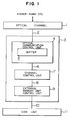
- Fig. 1 is a schematic diagram illustrating a disk unit sub-system according to an embodiment of the present invention.
- a disk control unit 3 includes an optical communication control unit 4 for controlling a communication protocol with a higher-rank optical channel 1, an external memory control unit 9 for controlling a lower-rank disk unit 11 and a channel control unit 7 communicating with both of them.
- the control units are connected through an optical fiber cable 2, a path 6 between the optical communication control unit and the channel control unit, a path 8 between the channel control unit and the external memory control unit, and a path 10 between the external memory control unit and the disk unit.
- the higher-rank optical channel 1 is connected to a higher-rank CPU (not shown).
- the optical communication control unit 4 includes a buffer 5 and stores write data from the higher-rank CPU through the optical channel 1 and read data from the disk unit 11 into the buffer 5 to thereby perform data transfer.
- the data stored in the buffer 5 is transferred to the channel control unit 7 or the higher-rank optical channel 1 by means of the hardware control of the optical communication control unit 4.
- Fig. 2 is a flow chart showing the write data transfer control of the optical communication control unit in the embodiment of the present invention.
- Fig. 3 is a detailed flow chart of the write data transfer control of the optical communication control unit in the embodiment of the present invention.
- the write data transfer control involves the data transfer control (step 101) of data for the buffer capacity or less at the beginning of the control, the data transfer control (step 102) before arrival of data, and the data transfer control (step 103) after arrival of data. After execution of the data transfer control, the data transfer is finished (step 104).
- the request of data for the capacity of the buffer 5 or less is indicated to the optical channel 1.
- step 101 the process proceeds to the data transfer control before arrival of data at the next step 102.
- the optical communication control unit 4 monitors a logical empty state of the buffer and indicates the data request to the optical channel 1.
- the data transfer from the buffer 5 to the channel control unit 7 by the physical hardware control is not performed yet before arrival of data and accordingly the empty state of the buffer 5 is monitored from an average data transfer speed of the hardware control for each transfer control request of data for the buffer capacity or less at step 101 to indicate the data request.
- the optical communication control unit 4 monitors the physical empty state of the buffer and indicates the data request to the optical channel 1.
- the data transfer from the buffer 5 to the channel control unit 7 by the hardware control is performed by the optical communication control unit 4 after arrival of the data and accordingly the empty state of the buffer 5 is monitored by the hardware control to indicate the data request for data left at steps 101 and 102.
- the buffer capacity B represents the number of data capable of being stored in the buffer 5.
- the packet capacity P represents the maximum number of data capable of being stored in a packet.
- a delivering timer value AT of the data number A represents a timer value (hour) of delivering data for the data number A starting from a final data request indication to proceed from step 102 to 103 on the basis of the average data transfer speed from the buffer 5 to the channel control unit 7 by the hardware control.
- a delivering timer value PT of the data number P represents a timer value (hour) of delivering data for the data number P from the buffer 5 starting from the final data request indication to proceed from step 102 to 103 on the basis of the average data transfer speed from the buffer 5 to the channel control unit 7 by the hardware control.
- step 101 of Fig. 2 the transfer control of write data for the capacity or less of the buffer 5 is first described.
- the write data transfer is started from step 200 in response to the transfer start indication of the write data to the optical communication unit 4 from the higher-rank optical channel 1.
- values A, B and P are set as the whole write data number, the buffer capacity, and the packet capacity, respectively (step 201).
- the request indication of data corresponding to the value A is performed to the higher-rank CPU (step 210) and the process proceeds to step 407.
- step 302 The values AT and PT for performing the data request indication are first set to timers (step 301). Then, as long as the value A is larger than or equal to the value P (A ⁇ P) (step 302), the logical buffer empty state is monitored in order to further perform the request of data requested up to step 206. That is, while the arrival of data is monitored (step 303), the arrival state to the buffer 5 of the data requested up to step 206 is monitored on the basis of the average data transfer speed of the hardware control.
- the request indication of data corresponding to the value P is performed to the higher-rank CPU (step 306) and the value P is subtracted from the value A (step 307).
- the monitoring of the data arrival and the delivering time of data corresponding to the value P is performed again (steps 303 - 305).
- step 303 When data at the head of the data requested at step 203 has arrived (step 303), the process proceeds to step 401. Then, when the remaining write data number from the higher-rank CPU is smaller than the packet capacity before arrival of data (step 302), the delivering time AT of data corresponding to the value A is monitored from the final data request indication at step 306 (step 308). The request indication of data number A is performed (step 310) to the higher-rank CPU and the process proceeds to step 407.
- step 401 sending of data to the channel control unit 7 by the hardware control is monitored from the final data request indication at step 306 and when the hardware has completed transfer of data corresponding to the value P to the channel control unit 7, the request indication of data corresponding to the value P is performed to the higher-rank CPU (step 402) and the value P is subtracted from the value A (step 403).
- step 401 - 403 As long as the value A is larger than or equal to the value P (A ⁇ P), the process at steps 401 - 403 is repeated.
- the value A is smaller than the value P, sending of data to the channel control unit 7 by the hardware control is monitored from the final data request indication and when the hardware has completed transfer of data corresponding to the value A to the channel control unit 7, the final request indication of data corresponding to the value A is performed to the higher-rank CPU (step 406) and the process proceeds to step 407.
- step 407 sending of data to the channel control unit 7 by the hardware control is monitored (step 407) and when data for the whole write data number can be sent to the channel control unit 7, the write data transfer is finished (step 408).
- This method is performed in order to improve the reliability of data transfer.
- a fixed transfer speed can be maintained by sending the request of a fixed amount of data at intervals of a fixed time.
Landscapes
- Engineering & Computer Science (AREA)
- Theoretical Computer Science (AREA)
- Physics & Mathematics (AREA)
- General Engineering & Computer Science (AREA)
- General Physics & Mathematics (AREA)
- Communication Control (AREA)
- Information Transfer Systems (AREA)
- Data Exchanges In Wide-Area Networks (AREA)
Applications Claiming Priority (3)
| Application Number | Priority Date | Filing Date | Title |
|---|---|---|---|
| JP24907793 | 1993-10-05 | ||
| JP249077/93 | 1993-10-05 | ||
| JP24907793 | 1993-10-05 |
Publications (3)
| Publication Number | Publication Date |
|---|---|
| EP0646871A2 true EP0646871A2 (fr) | 1995-04-05 |
| EP0646871A3 EP0646871A3 (fr) | 1996-07-31 |
| EP0646871B1 EP0646871B1 (fr) | 2003-11-26 |
Family
ID=17187666
Family Applications (1)
| Application Number | Title | Priority Date | Filing Date |
|---|---|---|---|
| EP94307121A Expired - Lifetime EP0646871B1 (fr) | 1993-10-05 | 1994-09-29 | Système à gérer le transfert de données |
Country Status (3)
| Country | Link |
|---|---|
| US (2) | US5623607A (fr) |
| EP (1) | EP0646871B1 (fr) |
| DE (1) | DE69433351T2 (fr) |
Families Citing this family (13)
| Publication number | Priority date | Publication date | Assignee | Title |
|---|---|---|---|---|
| US5991835A (en) * | 1994-11-22 | 1999-11-23 | Teac Corporation | Peripheral data storage device in which time interval used for data transfer from relatively fast buffer memory to relatively slower main memory is selected in view of average of time intervals during which data blocks were recently received from host |
| JP3190800B2 (ja) * | 1995-03-15 | 2001-07-23 | 甲府日本電気株式会社 | 転送速度切り替え機能付き非同期転送回路 |
| US5754771A (en) * | 1996-02-12 | 1998-05-19 | Sybase, Inc. | Maximum receive capacity specifying query processing client/server system replying up to the capacity and sending the remainder upon subsequent request |
| US6038620A (en) * | 1996-09-09 | 2000-03-14 | International Business Machines Corporation | Method and system for optimal high speed match in a high performance controller which ensures an input/output interface stays ahead of a host interface |
| US5878228A (en) * | 1996-11-15 | 1999-03-02 | Northern Telecom Limited | Data transfer server with time slots scheduling base on transfer rate and predetermined data |
| US6401167B1 (en) * | 1997-10-10 | 2002-06-04 | Rambus Incorporated | High performance cost optimized memory |
| AU9604698A (en) * | 1997-10-10 | 1999-05-03 | Rambus Incorporated | Method and apparatus for two step memory write operations |
| JP3569149B2 (ja) * | 1999-02-03 | 2004-09-22 | 株式会社日立製作所 | 通信制御装置 |
| US6993605B2 (en) | 2001-02-28 | 2006-01-31 | Sharp Laboratories Of America, Inc. | Adaptive run-time data transfer optimization |
| JP3703439B2 (ja) * | 2002-03-19 | 2005-10-05 | Necマイクロシステム株式会社 | データ転送制御装置及び方法 |
| CN1300703C (zh) * | 2003-11-05 | 2007-02-14 | 松下电器产业株式会社 | 调节电路及其具有它的功能处理电路 |
| US20050198459A1 (en) * | 2004-03-04 | 2005-09-08 | General Electric Company | Apparatus and method for open loop buffer allocation |
| JP4749002B2 (ja) * | 2005-02-25 | 2011-08-17 | ルネサスエレクトロニクス株式会社 | データ転送装置、画像処理装置及びデータ転送制御方法 |
Family Cites Families (16)
| Publication number | Priority date | Publication date | Assignee | Title |
|---|---|---|---|---|
| US3648247A (en) * | 1970-04-22 | 1972-03-07 | Scm Corp | Data handling system |
| NL165859C (nl) * | 1975-04-25 | 1981-05-15 | Philips Nv | Station voor informatie-overdracht. |
| US4258418A (en) * | 1978-12-28 | 1981-03-24 | International Business Machines Corporation | Variable capacity data buffer system |
| FR2466808A1 (fr) * | 1979-09-28 | 1981-04-10 | Ibm France | Systeme pour controler la duree de l'intervalle de temps entre blocs dans un systeme de communication calculateur a calculateur |
| JPS57179509A (en) * | 1981-04-28 | 1982-11-05 | Tokyo Shibaura Electric Co | Method of controlling temperature of superheated steam of boiler |
| US4860244A (en) * | 1983-11-07 | 1989-08-22 | Digital Equipment Corporation | Buffer system for input/output portion of digital data processing system |
| US5038277A (en) * | 1983-11-07 | 1991-08-06 | Digital Equipment Corporation | Adjustable buffer for data communications in a data processing system |
| US4901277A (en) * | 1985-09-17 | 1990-02-13 | Codex Corporation | Network data flow control technique |
| US4672613A (en) * | 1985-11-01 | 1987-06-09 | Cipher Data Products, Inc. | System for transferring digital data between a host device and a recording medium |
| US4860193A (en) * | 1986-05-22 | 1989-08-22 | International Business Machines Corporation | System for efficiently transferring data between a high speed channel and a low speed I/O device |
| JPH07122868B2 (ja) * | 1988-11-29 | 1995-12-25 | 日本電気株式会社 | 情報処理装置 |
| US4965793A (en) * | 1989-02-03 | 1990-10-23 | Digital Equipment Corporation | Method and apparatus for interfacing a system control unit for a multi-processor |
| US5117486A (en) * | 1989-04-21 | 1992-05-26 | International Business Machines Corp. | Buffer for packetizing block of data with different sizes and rates received from first processor before transferring to second processor |
| JPH077975B2 (ja) * | 1990-08-20 | 1995-01-30 | インターナショナル・ビジネス・マシーンズ・コーポレイション | データ伝送を制御するためのシステムおよび方法 |
| JPH04225452A (ja) * | 1990-12-27 | 1992-08-14 | Fujitsu Ltd | 光i/oインタフェース |
| US5247617A (en) * | 1991-02-26 | 1993-09-21 | Digi International, Inc. | Method for supplying data to a buffered uart |
-
1994
- 1994-09-29 US US08/314,782 patent/US5623607A/en not_active Expired - Lifetime
- 1994-09-29 DE DE69433351T patent/DE69433351T2/de not_active Expired - Fee Related
- 1994-09-29 EP EP94307121A patent/EP0646871B1/fr not_active Expired - Lifetime
-
1996
- 1996-12-18 US US08/769,217 patent/US5842042A/en not_active Expired - Lifetime
Also Published As
| Publication number | Publication date |
|---|---|
| EP0646871B1 (fr) | 2003-11-26 |
| DE69433351T2 (de) | 2004-05-27 |
| DE69433351D1 (de) | 2004-01-08 |
| US5623607A (en) | 1997-04-22 |
| EP0646871A3 (fr) | 1996-07-31 |
| US5842042A (en) | 1998-11-24 |
Similar Documents
| Publication | Publication Date | Title |
|---|---|---|
| EP0646871A2 (fr) | Système à gérer le transfert de données | |
| EP0009678B1 (fr) | Dispositif d'entrée/sortie pour ordinateur | |
| WO1998038580A1 (fr) | Determination dynamique de seuils de memoire tampon pour dispositif cible scsi | |
| US5129072A (en) | System for minimizing initiator processor interrupts by protocol controller in a computer bus system | |
| US4998246A (en) | Method for transmission of cyclic data | |
| US5878278A (en) | System for controlling connection requests by each IO controllers storing and managing a request queue wherein additional channel addresses can be added | |
| JP3517452B2 (ja) | データ転送制御方法 | |
| JPH1049344A (ja) | バッファのビジー制御方式 | |
| JP3221330B2 (ja) | バッファ制御方法 | |
| JPH06334705A (ja) | 通信制御装置 | |
| JP2584858B2 (ja) | 描画データ転送方式 | |
| JPH02268046A (ja) | パケット多重化装置 | |
| JPH02282855A (ja) | Dma転送制御方法 | |
| JPH0410652B2 (fr) | ||
| JPS5830256A (ja) | 通信制御装置 | |
| JPH02310649A (ja) | 受信フレーム転送方式および通信制御装置 | |
| JPH06195183A (ja) | プリンタ装置 | |
| JPS59173867A (ja) | デイスクキヤツシユデ−タ転送制御方式 | |
| JP2963229B2 (ja) | 磁気テープ記憶装置のテープマーク書込装置 | |
| JPS6158073A (ja) | デ−タ転送制御方式 | |
| JPS6294042A (ja) | 通信制御装置 | |
| JPS6269752A (ja) | デ−タ通信装置 | |
| JPH04317234A (ja) | 送信データのフロー制御方式 | |
| JPH06274440A (ja) | Scsiバス制御におけるsave data point処理方法 | |
| JPS60205628A (ja) | デ−タ転送方式 |
Legal Events
| Date | Code | Title | Description |
|---|---|---|---|
| PUAI | Public reference made under article 153(3) epc to a published international application that has entered the european phase |
Free format text: ORIGINAL CODE: 0009012 |
|
| 17P | Request for examination filed |
Effective date: 19940930 |
|
| AK | Designated contracting states |
Kind code of ref document: A2 Designated state(s): DE FR GB |
|
| PUAL | Search report despatched |
Free format text: ORIGINAL CODE: 0009013 |
|
| AK | Designated contracting states |
Kind code of ref document: A3 Designated state(s): DE FR GB |
|
| 17Q | First examination report despatched |
Effective date: 19991130 |
|
| GRAH | Despatch of communication of intention to grant a patent |
Free format text: ORIGINAL CODE: EPIDOS IGRA |
|
| GRAS | Grant fee paid |
Free format text: ORIGINAL CODE: EPIDOSNIGR3 |
|
| GRAA | (expected) grant |
Free format text: ORIGINAL CODE: 0009210 |
|
| AK | Designated contracting states |
Kind code of ref document: B1 Designated state(s): DE FR GB |
|
| REG | Reference to a national code |
Ref country code: GB Ref legal event code: FG4D |
|
| REF | Corresponds to: |
Ref document number: 69433351 Country of ref document: DE Date of ref document: 20040108 Kind code of ref document: P |
|
| ET | Fr: translation filed | ||
| PLBE | No opposition filed within time limit |
Free format text: ORIGINAL CODE: 0009261 |
|
| STAA | Information on the status of an ep patent application or granted ep patent |
Free format text: STATUS: NO OPPOSITION FILED WITHIN TIME LIMIT |
|
| 26N | No opposition filed |
Effective date: 20040827 |
|
| PGFP | Annual fee paid to national office [announced via postgrant information from national office to epo] |
Ref country code: FR Payment date: 20080814 Year of fee payment: 15 |
|
| PGFP | Annual fee paid to national office [announced via postgrant information from national office to epo] |
Ref country code: GB Payment date: 20080820 Year of fee payment: 15 |
|
| PGFP | Annual fee paid to national office [announced via postgrant information from national office to epo] |
Ref country code: DE Payment date: 20080908 Year of fee payment: 15 |
|
| GBPC | Gb: european patent ceased through non-payment of renewal fee |
Effective date: 20090929 |
|
| REG | Reference to a national code |
Ref country code: FR Ref legal event code: ST Effective date: 20100531 |
|
| PG25 | Lapsed in a contracting state [announced via postgrant information from national office to epo] |
Ref country code: FR Free format text: LAPSE BECAUSE OF NON-PAYMENT OF DUE FEES Effective date: 20090930 Ref country code: DE Free format text: LAPSE BECAUSE OF NON-PAYMENT OF DUE FEES Effective date: 20100401 |
|
| PG25 | Lapsed in a contracting state [announced via postgrant information from national office to epo] |
Ref country code: GB Free format text: LAPSE BECAUSE OF NON-PAYMENT OF DUE FEES Effective date: 20090929 |