EP0647018B1 - Digitaler Phasenkomparator - Google Patents
Digitaler Phasenkomparator Download PDFInfo
- Publication number
- EP0647018B1 EP0647018B1 EP94410083A EP94410083A EP0647018B1 EP 0647018 B1 EP0647018 B1 EP 0647018B1 EP 94410083 A EP94410083 A EP 94410083A EP 94410083 A EP94410083 A EP 94410083A EP 0647018 B1 EP0647018 B1 EP 0647018B1
- Authority
- EP
- European Patent Office
- Prior art keywords
- signal
- counter
- phase
- fref
- phase comparator
- Prior art date
- Legal status (The legal status is an assumption and is not a legal conclusion. Google has not performed a legal analysis and makes no representation as to the accuracy of the status listed.)
- Expired - Lifetime
Links
- 230000003247 decreasing effect Effects 0.000 claims description 2
- 238000012545 processing Methods 0.000 claims description 2
- 230000010363 phase shift Effects 0.000 claims 2
- 230000000630 rising effect Effects 0.000 description 16
- 238000010586 diagram Methods 0.000 description 13
- 238000012937 correction Methods 0.000 description 8
- 230000003071 parasitic effect Effects 0.000 description 4
- 238000010200 validation analysis Methods 0.000 description 4
- 238000005516 engineering process Methods 0.000 description 3
- 230000007257 malfunction Effects 0.000 description 2
- 238000000034 method Methods 0.000 description 2
- 244000045947 parasite Species 0.000 description 2
- 230000007704 transition Effects 0.000 description 2
- 230000002301 combined effect Effects 0.000 description 1
- 125000004122 cyclic group Chemical group 0.000 description 1
- 238000013479 data entry Methods 0.000 description 1
- 230000001934 delay Effects 0.000 description 1
- 238000013461 design Methods 0.000 description 1
- 235000021183 entrée Nutrition 0.000 description 1
- 230000007774 longterm Effects 0.000 description 1
- 238000005259 measurement Methods 0.000 description 1
- 238000012986 modification Methods 0.000 description 1
- 230000004048 modification Effects 0.000 description 1
Images
Classifications
-
- H—ELECTRICITY
- H03—ELECTRONIC CIRCUITRY
- H03D—DEMODULATION OR TRANSFERENCE OF MODULATION FROM ONE CARRIER TO ANOTHER
- H03D13/00—Circuits for comparing the phase or frequency of two mutually-independent oscillations
-
- H—ELECTRICITY
- H03—ELECTRONIC CIRCUITRY
- H03L—AUTOMATIC CONTROL, STARTING, SYNCHRONISATION OR STABILISATION OF GENERATORS OF ELECTRONIC OSCILLATIONS OR PULSES
- H03L7/00—Automatic control of frequency or phase; Synchronisation
- H03L7/06—Automatic control of frequency or phase; Synchronisation using a reference signal applied to a frequency- or phase-locked loop
- H03L7/08—Details of the phase-locked loop
- H03L7/085—Details of the phase-locked loop concerning mainly the frequency- or phase-detection arrangement including the filtering or amplification of its output signal
-
- H—ELECTRICITY
- H03—ELECTRONIC CIRCUITRY
- H03B—GENERATION OF OSCILLATIONS, DIRECTLY OR BY FREQUENCY-CHANGING, BY CIRCUITS EMPLOYING ACTIVE ELEMENTS WHICH OPERATE IN A NON-SWITCHING MANNER; GENERATION OF NOISE BY SUCH CIRCUITS
- H03B2200/00—Indexing scheme relating to details of oscillators covered by H03B
- H03B2200/006—Functional aspects of oscillators
- H03B2200/008—Functional aspects of oscillators making use of a reference frequency
Definitions
- the present invention relates to locking loops phase (PLL), and in particular a phase comparator digital used in a PLL of which all the elements are realized digitally.
- PLL locking loops phase
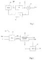
- FIG. 1 schematically represents a conventional PLL architecture.
- the PLL comprises a voltage controlled oscillator (VCO) 10 delivering a frequency NF to a divider by N 12.
- VCO voltage controlled oscillator
- a phase comparator 14 receives the output frequency F of the divider 12 and a reference frequency Fref.
- the phase comparator 14 supplies a phase error signal e to a filter 16 whose output c controls the oscillator 10.
- the signal F is calibrated in phase and in frequency on the signal Fref.
- the frequency F to be obtained is of the order of 15 kHz
- the frequency NF of the order of 12 MHz (N 768)
- the filter 16 is a low-pass filter with a cutoff frequency of a few hundred hertz.
- FIG. 2 shows a phase comparator 14 classic digital.
- This phase comparator includes a detector / frequency (PFD) 18 receiving the Fref and F. It provides UP pulses of widths equal to the delays phase of signal F with respect to signal Fref, and pulses DOWN of widths equal to the phase advances of signal F compared to the Fref signal.
- An up / down counter 20 receives a CK clock signal of high frequency compared to that of Fref and F signals. The up / down counting 20 is validated by UP pulses, and counting by pulses DOWN.
- a sequencer 22 receiving the signals F and CK, resets at zero the up / down counter 20 between two edges of the signal F, after the content of it is processed by the filter.
- up / down counter 20 contains a numerical value E corresponding to the phase error sought.
- each UP or DOWN pulse correspond respectively to an edge of the Fref signal and to an edge of signal F.
- the UP pulse or DOWN then generated is shortened or lengthened so wrong.
- Such a phase comparator is not suitable for process horizontal scanning signals in a television, because the Fref signal can then include many pulses parasites.
- the clock signal CK must be of frequency particularly high.
- the frequency of this CK signal must be of the order of 200 megahertz.
- Current technologies do not allow not to realize such a fast up / down counter.
- U.S. Patent 4,351,002 describes a comparator of digital phase providing numerical values corresponding to phase differences between a first signal and a second signal, including a one-way counter initialized at the frequency of first signal and clocked by a high frequency clock signal compared to that of the first and second signals, and a logic gate to validate the counter.
- the edges of the first and second signals cause state changes of flip-flops, and these are the states of these flip-flops which determine the validation or not of the counter via of the logic gate.
- this phase comparator is sensitive to fronts of the first and second signals and therefore has the disadvantage to be sensitive to parasitic impulses.
- An object of the present invention is to provide a digital phase comparator that can operate with a frequency particularly high clock.
- Another object of the present invention is to achieve a digital phase comparator little sensitive to pulses parasites.
- phase comparator digital device described in claim 1 and similar to that of the aforementioned US patent and which differs in that the first signal has a duty cycle substantially equal to 0.5 and in that the logic gate is connected to validate the counter when the first and second signals are at predetermined respective states, a phase difference being considered null when it corresponds to half the meter capacity.
- the comparator comprises a rocker cooperating with said logic gate to validate the counter only when a predetermined edge of the second signal arrives when the first signal is in its predetermined state respective.
- the comparator comprises a circuit for processing the first signal for decrease the duration of the respective predetermined state thereof duration corresponding to counting by the counter up to half of his capacity.
- the comparator includes a clock generator providing several clock signals of the same frequency but phase shifted of a constant value, these clock signals being successively supplied to the counter at the frequency of the first signal.
- a comparator of digital phase uses a sense counter single 30 which has the advantage, if it is asynchronous, of being able operate with a frequency clock signal CK also high than about 200 MHz in current technologies current (which is not the case of down-counters).
- the counter 30 receives the output of an AND gate 32 receiving on an input the signal Fref and on another input the signal F inverted.
- the validation signal EN supplied by gate 32 is sensitive to the states of the Fref signals and F and not at their fronts; if one of the signals Fref and F presents a parasitic pulse, the validation signal EN is active only for the duration of the parasitic pulse and the content of counter 30 varies very little.
- the counter 30 is reset periodically by a CLR signal supplied by a sequencer 22 receiving the F and CK signals.
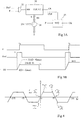
- FIG. 3B illustrates an example of signal shape F and Fref and the corresponding variation of the content E0 of the counter 30.
- the signal F supplied by the divider 12 (FIG. 1) of a PLL, has a duty cycle of 0.5.
- the Fref signal corresponds to synchronization pulses of assumed constant width (approximately 4.7 microseconds).
- the frequency of the CK clock is chosen so that the counter counts up to its maximum value (511) for the duration of a pulse of the Fref signal. So if a pulse of the Fref signal is centered on a rising edge of the signal F, the counter reaches a value (256) equal to half of its capacity. This half value is chosen to match at zero phase error; we synchronize the fronts amounts of signal F on the centers of the signal pulses Fref.
- the sequencer 22 resets the counter 30 to zero. The instant t 3 occurs before the next rising edge of the signal F.
- the counter reaches its maximum value 511 which corresponds to a negative maximum phase error -Emax (phase delay of the signal F with respect to the signal Fref) .
- the counter 30 is established at a value between its zero value and its maximum value, corresponding to a phase error E proportional to the phase error real. For example, at an instant t 4 , a rising edge of the signal F occurs shortly before the end of a pulse of the signal Fref. The counter 30 reaches a value close to 511 corresponding to a negative phase error E and proportional to the real phase error.
- FIG. 4 represents a diagram of the error of phase E provided by the phase comparator of FIG. 3A in function of the actual phase error Er. This diagram is symmetrical relative to the origin of the diagram. Around the value 0, the error E varies in proportion to the actual error Er. Beyond this linear area, the error E saturates at its value maximum positive or at its maximum negative value.
- phase comparator If a phase comparator according to the invention is used in the PLL of a horizontal TV scanning system, linear ranges are only about 4.7 microseconds on the 64 microseconds of a signal period Fref. This would suggest that the PLL cannot converge if the signal F is initially arbitrary.
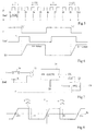
- FIG. 5 is used to show that such a PLL ends up converge.
- the period of signal F is initially equal to 1.
- the signal period Fref is constant and equal to 1.25.
- the pulse centers of the Fref signal are represented by vertical bars I1, I2 ... Under each bar, there is shown the corresponding sign of error E.
- PLL filter 16 is a correction filter proportional and integral.
- the filter time constant is particularly high, which means that the correction integral only works in the long term, when a large number of same sign values of the phase error are provided. So, for simplicity, we can assume below that this correction integral does not intervene.
- the phase error values are maximum, which is not far from reality because there is a high probability, when the signal F is arbitrary, that the centers of the pulses of the Fref signal occur in the saturation ranges of the figure 4.
- the filter 16 acts on the oscillator 10, which is a frequency synthesizer in a PLL entirely digital, so as to correct the period of signal F with a constant (low) value in the same direction as phase E error, the correction occurring, for example, at rising edge of signal F occurring after error measurement.
- the pulses I1 and I2 occur when the signal F is 0.
- the corresponding E errors are negative.
- the period of signal F is set to 1 when it was previously slightly higher.
- the period of signal F is maintained at 1 as long as the phase error is negative.
- Pulse I3 occurs when signal F is at 1. The corresponding error E is positive. This pulse I3 is fairly close to a preceding rising edge of signal F; if the signal period F had not been reduced, pulse I3 could have occurred when the signal F was at 0 and produce a negative E error. The period of signal F goes from 1 to 1.125 at the rising edge of signal F following pulse I3.
- the I4 and I5 pulses also occur when signal F is at 1; the corresponding error is positive and the signal F keeps the period of 1.125. Pulse I5 occurs just before a falling edge of signal F. If the period of signal F had not been increased, pulse I5 could have occur when signal F was at 0 and produce an error E negative.
- the pulses I6 and I7 occur when the signal F is at 0, the corresponding error E is negative and the period of signal F becomes 1 at the rising edge following pulse I6.
- the pulses I8 to I10 occur when the signal F is at 1, and the period of signal F becomes 1.125 at the edge amount following pulse I8.
- Figure 6 illustrates a situation where the pulses of the Fref signal have any width, and in any case greater to that corresponding to a count up to the value maximum of the counter 30.
- the phase comparator of Figure 3A in some cases works erroneously.
- this kind of error is likely to occur when the pulses of the Fref signal are wider than that corresponding to a count up to the maximum value of counter 30.
- This error is therefore likely to happen, as shown right of Figure 6, in a common case (other than in a scan where the F and Fref signals are related cyclic 0.5.
- a phase comparator according to the invention makes it possible to synchronize the rising edges of the signal F at a predetermined position at the start of games at 1 of the signal Fref, and not on the center of these parts. This case is particularly unfavorable because we can detect, like this is shown, a maximum delay of the signal F while the latter is only slightly ahead.
- FIG. 7 represents an embodiment of digital phase comparator according to the invention allowing avoid the aforementioned drawback.
- a door 32 receives, at the instead of the inverse of the signal F, the output Q of a flip-flop 34.
- the data entry D of this flip-flop receives the value 1, the clock input the Fref signal, and the reset input at 0 R signal F.
- counter 30 is validated only if a rising edge of the Fref signal then occurs signal F is 0. This removes erroneous counts from Figure 6.
- Figure 8 shows the diagram of error E supplied as a function of the actual error Er, obtained with the comparator in Figure 7. This diagram is not symmetrical and exhibits an abrupt transition at points where a falling edge of signal F occurs at the same time as a falling edge of the Fref signal (before the abscissa - ⁇ and ⁇ ).
- the diagram is made symmetrical, as shown in dotted lines, decreasing the time to 0 of signal F of the duration corresponding to the counting of the counter 30 up to half its capacity.
- This can be achieved, by example, as shown in Figure 7, treating the signal F in the sequencer 22 before supplying it to the scale 34 so as to delay its falling fronts by 256 periods the CK clock (in the example where the maximum value of the counter 30 is 511).
- the resolution of the phase comparator described so far is of a clock period CK, that is to say that in regime established, the value of the phase error oscillates between -1 and +1.
- the average resolution of the comparator can be improved thanks to the configuration described below.
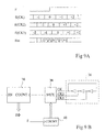
- FIG. 9A illustrates the operation of a PLL provided a phase comparator according to the invention in steady state.
- the result E (CK) provided by the comparator can be symbolized by a graduated rule ...- 1, 0, +1, +2 ...
- the value supplied as that phase error E corresponds to the graduation opposite which occurs a rising edge of the Fref signal.
- a rising edge of the Fref signal occurs opposite graduation 0, which provides a phase error of 0.
- the frequency of signal F is never exactly what it should be, and the rising front moves around 0 along the rule, so that errors provided tend to fluctuate between -1 and +1.
- the phase comparator proposes to increase the accuracy of errors E on average supplied by the phase comparator.
- CK three rules, rule E (CK) above and two additional rules E (CK2) and E (CK3) shifted one by compared to the previous one-third graduation.
- These rules are used cyclically to provide error E.
- the first rule provides the value 0
- the second rule also provides the value 0
- the third rule provides the value -1. So, if the signal F remains stable, the phase comparator provides the value -1 once in three, which corresponds on average to a phase error of -1/3.
- rule E CK3
- Em a rule Em corresponding to the average phase errors which are obtains every three periods of signal F.
- FIG. 9B represents an embodiment of phase comparator according to the invention making it possible to increase the accuracy of the comparator according to what has been described above.
- a oscillator 36 provides three clock signals CK, CK2, CK3 from same frequency and phase shifted by a third of a period one by compared to each other.
- the oscillator 36 is for example an oscillator in a ring with three inverters whose outputs provide the signals CK, CK2, CK3 respectively.
- a multiplexer 38 receives these three clock signals and supplies only one to the counter 30.
- the clock signal to be supplied is selected by a counter up to three 40 receiving as a signal clock signal F.
Landscapes
- Engineering & Computer Science (AREA)
- Power Engineering (AREA)
- Stabilization Of Oscillater, Synchronisation, Frequency Synthesizers (AREA)
Claims (4)
- Digitaler Phasenkomparator zur Bildung von Digitalwerten (E) entsprechend den Phasenunterschieden zwischen einem ersten Signal (F) und einem zweiten Signal (Fref), welcher einen nur in einer Richtung arbeitenden Zähler (30), welcher mit der Frequenz des ersten Signals initialisiert und durch ein Taktsignal (CK) von hoher Frequenz relativ bezüglich der Frequenz des ersten und des zweiten Signals getaktet wird, sowie ein logisches Gatter (32) zur Aktivierung des Zählers aufweist,
dadurch gekennzeichnet, daß das erste Signal ein Impulstastverhältnis im wesentlichen gleich 0,5 aufweist und daß das logische Gatter (32) so geschaltet ist, daß es den Zähler aktiviert, sobald sich das erste und das zweite Signal in jeweils vorgegebenen Zuständen befinden, wobei eine Phasendifferenz als Null betrachtet wird, sobald sie dem halben Wert der Zählkapazität des Zählers entspricht. - Phasenkomparator nach Anspruch 1,
dadurch gekennzeichnet, daß er eine Kippschaltung (34) aufweist, welche mit dem genannten logischen Gatter (32) zusammenwirkt, derart daß der Zähler (30) nur dann aktiviert wird, wenn eine vorgegebene Flanke des zweiten Signals (Fref) auftritt, während sich das erste Signal in seinem betreffenden vorgegebenen Zustand befindet. - Phasenkomparator nach Anspruch 2,
dadurch gekennzeichnet, daß er eine Schaltung (22) zur Bearbeitung des ersten Signals (F) umfaßt, um die Dauer des betreffenden vorgegebenen Zustands dieses Signals um die Dauer, welche dem Zählvorgang des Zählers (30) bis zu seiner halben Zählkapazität entspricht, zu verringern. - Phasenkomparator nach Anspruch 1 oder 2,
dadurch gekennzeichnet, daß er einen Taktgenerator zur Erzeugung mehrerer Taktsignale (CK, CK2, CK3) von gleicher Frequenz, die jedoch gegeneinander in der Phase um einen konstanten Wert versetzt sind, aufweist, und daß diese Taktsignale aufeinanderfolgend dem Zähler mit der Frequenz des ersten Signals zugeführt werden.
Applications Claiming Priority (2)
| Application Number | Priority Date | Filing Date | Title |
|---|---|---|---|
| FR9311864A FR2710797B1 (fr) | 1993-09-30 | 1993-09-30 | Comparateur de phase numérique. |
| FR9311864 | 1993-09-30 |
Publications (2)
| Publication Number | Publication Date |
|---|---|
| EP0647018A1 EP0647018A1 (de) | 1995-04-05 |
| EP0647018B1 true EP0647018B1 (de) | 1998-04-29 |
Family
ID=9451556
Family Applications (1)
| Application Number | Title | Priority Date | Filing Date |
|---|---|---|---|
| EP94410083A Expired - Lifetime EP0647018B1 (de) | 1993-09-30 | 1994-09-27 | Digitaler Phasenkomparator |
Country Status (5)
| Country | Link |
|---|---|
| US (1) | US5563531A (de) |
| EP (1) | EP0647018B1 (de) |
| JP (1) | JP3786440B2 (de) |
| DE (1) | DE69409903T2 (de) |
| FR (1) | FR2710797B1 (de) |
Families Citing this family (9)
| Publication number | Priority date | Publication date | Assignee | Title |
|---|---|---|---|---|
| US6121816A (en) * | 1999-04-23 | 2000-09-19 | Semtech Corporation | Slave clock generation system and method for synchronous telecommunications networks |
| JP3665512B2 (ja) * | 1999-07-12 | 2005-06-29 | 株式会社東芝 | 二値信号の比較装置及びこれを用いたpll回路 |
| US6826247B1 (en) | 2000-03-24 | 2004-11-30 | Stmicroelectronics, Inc. | Digital phase lock loop |
| US6628276B1 (en) | 2000-03-24 | 2003-09-30 | Stmicroelectronics, Inc. | System for high precision signal phase difference measurement |
| US6661295B2 (en) | 2001-04-09 | 2003-12-09 | Cts Corporation | Controllable crystal oscillator |
| US6946919B2 (en) * | 2002-01-14 | 2005-09-20 | Cts Corporation | Controllable crystal oscillator component |
| US6930516B2 (en) | 2001-05-30 | 2005-08-16 | Agere Systems Inc. | Comparator circuits having non-complementary input structures |
| US6597225B1 (en) | 2002-03-22 | 2003-07-22 | Agere Systems Inc. | Data capture circuit with series channel sampling structure |
| US6700448B1 (en) | 2002-08-30 | 2004-03-02 | Cts Corporation | High performance dual range oscillator module |
Family Cites Families (4)
| Publication number | Priority date | Publication date | Assignee | Title |
|---|---|---|---|---|
| FR2474794A1 (fr) * | 1980-01-25 | 1981-07-31 | Labo Electronique Physique | Circuit de correction des ecarts de phase entre les signaux de commande de balayage et les signaux de synchronisation lignes dans un recepteur de television |
| DE3443925C1 (de) * | 1984-12-01 | 1986-01-30 | Philips Patentverwaltung Gmbh, 2000 Hamburg | Schaltungsanordnung zum Unterscheiden der beiden Halbbilder in einem Fernsehsignal |
| US4654586A (en) * | 1985-06-10 | 1987-03-31 | The United States Of America As Represented By The Secretary Of The Air Force | Digital phase meter apparatus |
| JP2980267B2 (ja) * | 1992-01-20 | 1999-11-22 | 日本電信電話株式会社 | 位相比較回路およびこれを用いた位相同期発振回路 |
-
1993
- 1993-09-30 FR FR9311864A patent/FR2710797B1/fr not_active Expired - Fee Related
-
1994
- 1994-09-15 US US08/306,482 patent/US5563531A/en not_active Expired - Lifetime
- 1994-09-27 DE DE69409903T patent/DE69409903T2/de not_active Expired - Fee Related
- 1994-09-27 EP EP94410083A patent/EP0647018B1/de not_active Expired - Lifetime
- 1994-09-29 JP JP23481094A patent/JP3786440B2/ja not_active Expired - Fee Related
Also Published As
| Publication number | Publication date |
|---|---|
| DE69409903T2 (de) | 1998-08-27 |
| FR2710797A1 (fr) | 1995-04-07 |
| US5563531A (en) | 1996-10-08 |
| DE69409903D1 (de) | 1998-06-04 |
| EP0647018A1 (de) | 1995-04-05 |
| JP3786440B2 (ja) | 2006-06-14 |
| JPH07162298A (ja) | 1995-06-23 |
| FR2710797B1 (fr) | 1995-12-15 |
Similar Documents
| Publication | Publication Date | Title |
|---|---|---|
| EP0647018B1 (de) | Digitaler Phasenkomparator | |
| FR2498032A1 (fr) | Synchroniseur de bits pour signaux numeriques | |
| FR2790152A1 (fr) | Dispositif de suppression de decalage d'horloge | |
| FR2554994A1 (fr) | Dispositif de generation d'une frequence fractionnaire d'une frequence de reference | |
| EP0735694B1 (de) | Kostengünstige integrierbare Vorrichtung zur Verarbeitung elektrischer Signale nach der ARINC-429-Norm | |
| EP4354279B1 (de) | Erzeugung von echten zufallszahlen mit kohärenter abtastung in fd-soi-technologie | |
| EP1424774B1 (de) | Zufallszahlengenerator | |
| EP0680170B1 (de) | Übertragungsanordnung für ein Leitungskodiertes Signal über eine Fernsprechleitung mit Frequenzsynchronisierungsschaltung | |
| FR2553542A1 (fr) | Circuit integre a semi-conducteurs | |
| EP4390665B1 (de) | Entropiequelle mit on-board-berechnungsverfahren zur erzeugung von echten zufallszahlen | |
| EP0023852B1 (de) | Verfahren und Vorrichtung zur Phasenregelung eines lokalen Taktgebers | |
| EP0753941A1 (de) | Frequenzsynthetisierer | |
| FR2898743A1 (fr) | Compteur avec circuit de correction | |
| FR2773925A1 (fr) | Synthetiseur de frequence a boucle d'asservissement en phase avec circuit de detection d'asservissement | |
| EP0134374B1 (de) | Phasenverriegelter Taktgeber | |
| FR2610154A1 (fr) | Generateur de signaux de cadencement, notamment pour les systemes informatises de test de circuits integres | |
| EP0526359B1 (de) | Verfahren und Schaltungsanordnung zur Synchronisierung eines Signals | |
| EP0289385B1 (de) | Referenzzeitvorrichtung mit konstanter Stabilität für Kurz- und Langzeitmessungen | |
| FR2782387A1 (fr) | Circuit de detection de la disparition d'un signal periodique | |
| EP2327160A1 (de) | Analogzähler und ein einen solchen zähler enthaltenden bildgeber | |
| EP0644654B1 (de) | Digitaler Integrator und Filter erster Ordnung | |
| EP1291817B1 (de) | Nachweis von Umgebungsvariationen in einer Integrierten Schaltung | |
| EP0092879B1 (de) | Bitsynchronisiereinrichtung für Modulator-Demodulator oder Empfänger von Datenübertragung | |
| EP1073204A1 (de) | Anordnung zur Synchronisierung eines Bezugselements eines analogen Signals mit einem Taktsignal | |
| FR3025901A1 (fr) | Dispositif de generation d'un signal d'horloge par multiplication de frequence |
Legal Events
| Date | Code | Title | Description |
|---|---|---|---|
| PUAI | Public reference made under article 153(3) epc to a published international application that has entered the european phase |
Free format text: ORIGINAL CODE: 0009012 |
|
| AK | Designated contracting states |
Kind code of ref document: A1 Designated state(s): DE FR GB IT |
|
| 17P | Request for examination filed |
Effective date: 19950905 |
|
| 17Q | First examination report despatched |
Effective date: 19961022 |
|
| GRAG | Despatch of communication of intention to grant |
Free format text: ORIGINAL CODE: EPIDOS AGRA |
|
| GRAG | Despatch of communication of intention to grant |
Free format text: ORIGINAL CODE: EPIDOS AGRA |
|
| GRAH | Despatch of communication of intention to grant a patent |
Free format text: ORIGINAL CODE: EPIDOS IGRA |
|
| GRAH | Despatch of communication of intention to grant a patent |
Free format text: ORIGINAL CODE: EPIDOS IGRA |
|
| GRAA | (expected) grant |
Free format text: ORIGINAL CODE: 0009210 |
|
| AK | Designated contracting states |
Kind code of ref document: B1 Designated state(s): DE FR GB IT |
|
| REF | Corresponds to: |
Ref document number: 69409903 Country of ref document: DE Date of ref document: 19980604 |
|
| GBT | Gb: translation of ep patent filed (gb section 77(6)(a)/1977) |
Effective date: 19980605 |
|
| ITF | It: translation for a ep patent filed | ||
| RAP4 | Party data changed (patent owner data changed or rights of a patent transferred) |
Owner name: STMICROELECTRONICS S.A. |
|
| PLBE | No opposition filed within time limit |
Free format text: ORIGINAL CODE: 0009261 |
|
| STAA | Information on the status of an ep patent application or granted ep patent |
Free format text: STATUS: NO OPPOSITION FILED WITHIN TIME LIMIT |
|
| 26N | No opposition filed | ||
| REG | Reference to a national code |
Ref country code: GB Ref legal event code: IF02 |
|
| PGFP | Annual fee paid to national office [announced via postgrant information from national office to epo] |
Ref country code: DE Payment date: 20031009 Year of fee payment: 10 |
|
| PG25 | Lapsed in a contracting state [announced via postgrant information from national office to epo] |
Ref country code: DE Free format text: LAPSE BECAUSE OF NON-PAYMENT OF DUE FEES Effective date: 20050401 |
|
| PGFP | Annual fee paid to national office [announced via postgrant information from national office to epo] |
Ref country code: FR Payment date: 20050823 Year of fee payment: 12 |
|
| PGFP | Annual fee paid to national office [announced via postgrant information from national office to epo] |
Ref country code: GB Payment date: 20050921 Year of fee payment: 12 |
|
| PG25 | Lapsed in a contracting state [announced via postgrant information from national office to epo] |
Ref country code: IT Free format text: LAPSE BECAUSE OF NON-PAYMENT OF DUE FEES;WARNING: LAPSES OF ITALIAN PATENTS WITH EFFECTIVE DATE BEFORE 2007 MAY HAVE OCCURRED AT ANY TIME BEFORE 2007. THE CORRECT EFFECTIVE DATE MAY BE DIFFERENT FROM THE ONE RECORDED. Effective date: 20050927 |
|
| GBPC | Gb: european patent ceased through non-payment of renewal fee |
Effective date: 20060927 |
|
| REG | Reference to a national code |
Ref country code: FR Ref legal event code: ST Effective date: 20070531 |
|
| PG25 | Lapsed in a contracting state [announced via postgrant information from national office to epo] |
Ref country code: GB Free format text: LAPSE BECAUSE OF NON-PAYMENT OF DUE FEES Effective date: 20060927 |
|
| PG25 | Lapsed in a contracting state [announced via postgrant information from national office to epo] |
Ref country code: FR Free format text: LAPSE BECAUSE OF NON-PAYMENT OF DUE FEES Effective date: 20061002 |