EP0647026A2 - Dispositif de protection contre la surintensité pour transistor - Google Patents
Dispositif de protection contre la surintensité pour transistor Download PDFInfo
- Publication number
- EP0647026A2 EP0647026A2 EP94115435A EP94115435A EP0647026A2 EP 0647026 A2 EP0647026 A2 EP 0647026A2 EP 94115435 A EP94115435 A EP 94115435A EP 94115435 A EP94115435 A EP 94115435A EP 0647026 A2 EP0647026 A2 EP 0647026A2
- Authority
- EP
- European Patent Office
- Prior art keywords
- transistor
- gate
- current
- main
- main transistor
- Prior art date
- Legal status (The legal status is an assumption and is not a legal conclusion. Google has not performed a legal analysis and makes no representation as to the accuracy of the status listed.)
- Granted
Links
Images


Classifications
-
- H—ELECTRICITY
- H03—ELECTRONIC CIRCUITRY
- H03K—PULSE TECHNIQUE
- H03K17/00—Electronic switching or gating, i.e. not by contact-making and –breaking
- H03K17/08—Modifications for protecting switching circuit against overcurrent or overvoltage
- H03K17/082—Modifications for protecting switching circuit against overcurrent or overvoltage by feedback from the output to the control circuit
- H03K17/0822—Modifications for protecting switching circuit against overcurrent or overvoltage by feedback from the output to the control circuit in field-effect transistor switches
-
- H—ELECTRICITY
- H03—ELECTRONIC CIRCUITRY
- H03F—AMPLIFIERS
- H03F1/00—Details of amplifiers with only discharge tubes, only semiconductor devices or only unspecified devices as amplifying elements
- H03F1/52—Circuit arrangements for protecting such amplifiers
-
- H—ELECTRICITY
- H03—ELECTRONIC CIRCUITRY
- H03K—PULSE TECHNIQUE
- H03K17/00—Electronic switching or gating, i.e. not by contact-making and –breaking
- H03K17/08—Modifications for protecting switching circuit against overcurrent or overvoltage
- H03K17/082—Modifications for protecting switching circuit against overcurrent or overvoltage by feedback from the output to the control circuit
- H03K17/0828—Modifications for protecting switching circuit against overcurrent or overvoltage by feedback from the output to the control circuit in composite switches
-
- H—ELECTRICITY
- H10—SEMICONDUCTOR DEVICES; ELECTRIC SOLID-STATE DEVICES NOT OTHERWISE PROVIDED FOR
- H10D—INORGANIC ELECTRIC SEMICONDUCTOR DEVICES
- H10D89/00—Aspects of integrated devices not covered by groups H10D84/00 - H10D88/00
- H10D89/60—Integrated devices comprising arrangements for electrical or thermal protection, e.g. protection circuits against electrostatic discharge [ESD]
Definitions
- the present invention relates to an over current protection device for an insulated gate controlled transistor such as a power MOS transistor, an insulated gate bipolar transistor, etc..
- insulated gate controlled transistors Since the input impedance of insulated gate controlled transistors is very high, since power MOS transistors are applicable in a high frequency range and since insulated gate bipolar transistors, the output impedance of which is very low, are well suited for large current applications, these insulated gate controlled transistors are widely used in a form of a vertical element in a switching power supply, an inverter for controlling a motor, etc..
- a power transistor requires some protection measures against an over current since the power transistor is damaged or broken down rather easily by an over current caused by an abnormality on the load side.
- the protection measures have been incorporated into an integrated circuit together with related circuits.
- a protection scheme has been known which incorporates a current detector transistor as an over current protection means with a main transistor and executes protection by detecting an over current flowing through the main transistor on the basis of the principle of the Miller's current circuit. This protection scheme is described, for example, in Electro mini/micro Northeast Conf. Rec. E 10.4.1-10.4.4., 1986 by D. L. Zaremba Jr. and in the US Patent No. 4,783,690.
- Figure 6 schematically shows the protection technique according to this prior art.
- a load power supply 2 supplies voltage of typically several hundreds of volts to a load 1.
- a main transistor 10 which controls a current flowing through the load 1 is a power MOS transistor, the drain terminal D of which is connected with the load 1 and the source terminal S of which is grounded.
- the main transistor 10 is usually comprised of many unit structures connected in parallel with each other and incorporated into a semiconductor device.
- a current detector transistor 20 is comprised of from one to several unit structures, assigned to the current detection purpose, having the same unit structure with the unit structure of the main transistor 10 and being incorporated into the semiconductor device.
- the drain and the gate of the current detector transistor 20 are connected in common to the the drain and the gate of the main transistor 10, respectively.
- the common gate receives a drive command Ss from a drive circuit 3.
- a gate resistor Rg is connected as shown in Fig. 6 to the common gate for adjusting the speed of current changes (di/dt) supplied to the load 1.
- a small follower current i of one several thousandth of a reference current l of the main transistor 10 flows through the current detector transistor 20.
- the follower current i is detected as a voltage drop across a current detecting means Rd connected to the source of the current detector transistor 20.
- An operational amplifier 30 compares a detection signal Vd indicative of the voltage drop with a reference voltage Vr and outputs a comparison signal Sd indicative of the result of the comparison to a gate control circuit 40.
- the control circuit 40 outputs a control signal Sc to the common gate of the transistors 10 and 20 based on the comparison signal Sd.
- the detection signal Vd exceeds the reference voltage Vr and the control circuit 40 which receives the comparison signal Sd from the operational amplifier 30 outputs the control signal Sc to the main transistor 10 to limit or shut off the current l flowing through the main transistor 10.
- the control signal Sc lowers the HIGH signal or changes the HIGH signal to the LOW signal.
- the over current protection device protects the main transistor from an over current by correctly detecting the current l of the main transistor 10 by means of the current i of the detector transistor 20 based on the principle of the Miller's current circuit.
- oscillation tends to occur in the prior art circuit when the main transistor is of large current capacity and has a large electrostatic capacitance. This is because, though the feedback control system including the operational amplifier 30 which receives the detection signal Vd and the control circuit 40, shows quick response and high gain, the controlled system including the gate capacitance and the gate resistor Rg of the main and current detector transistors 10 and 20 can not quickly follow the control signals Sc.
- the simplest measure for preventing the oscillation is to lower the responsiveness and the gain of the feedback system, but this preventive measure causes insufficient over current detection sensitivity and too slow protective operation which in turn may cause damage or breakdown of the main transistor 10.
- Another measure for solving this problem has been known which provides the operational amplifier 30 with a phase compensation function (see for example "Circuit Techniques For Fully Utilizing Operational Amplifiers" by Iwao Sagara, pp14-15, published in 1987 from Nikkan Kougyou). This phase compensation technique will be briefly explained below with reference to Fig. 7.
- the operational amplifier 30 illustrated in Fig. 7 is comprised of a differential input block 31 which receives the detected voltage Vd and the reference voltage Vr; an amplifying block 32 which receives the output of the differential input block 31; and an output block 33 which is driven by the amplifying block 32 and outputs the comparison signal Sd.
- a phase compensation capacitor Cp is connected, for example on the input side of a transistor of the amplifying block 32 as shown in the figure.
- the phase compensation capacitor Cp shifts the phase of change of the comparison signal Sd corresponding to a change of the detected voltage Vd.
- the oscillation is prevented, without so much deteriorating the protective function, by appropriately adjusting the phase delay to the response delay caused by the gate capacitance of the main transistor 10 of the controlled system.
- an object of the present invention is to provide an over current protection device for a transistor which is free from oscillation, well suited for practical use and simply configured.
- the main transistor is a transistor which is controlled through its insulated gate, such as a MOS transistor, insulated gate bipolar transistor, etc., and is very often comprised of many repeated unit structures, it is preferable to assign one of the unit structures to the current detector transistor. It is simple but sufficient to use a resistor as the current detecting means.
- the over current protection device of the present invention which is comprised of a semiconductor base plate into which the main transistor and the current detector transistor are built in side by side to form a respective channel portion in a surface portion of the base plate; and an insulative film covering surface portions between the main transistor and the current detector transistor, in which the gate of the current detector transistor is extended to cover the insulative film.
- the insulative film is preferably thick enough like a field oxide film.
- the present invention which is based on the finding that oscillation in gate control is prevented simply by improving response of the gate control on the side of the current detector transistor, has solved the aforementioned problem by separating the gate of the current detector transistor from the gate of the main transistor, by setting the time constant of the detector transistor gate circuit at a shorter value than, preferably at less than one tenth of, the time constant of the main transistor gate circuit, and by feeding the control signal output from the feedback system which includes the current detecting means and the gate control means to the detector transistor gate circuit.
- the prior art has adopted a common gate, which is disposed commonly to the main and current detector transistors and which provides the gate circuits of the main and current detector transistors with the same time constant. According to the prior art, since the feedback system with quick response and with high gain controls the gates uselessly or forcibly based on the result of current detection of slow response, oscillation in the gate control tends to occur.
- the proportionality between the currents of the main and current detector transistors based on the principle of the Miller's current circuit is maintained with almost no trouble, except during a limited transient period, since, in the present invention, the gate of the current detector transistor is connected to the gate of the main transistor through its gate resistor, since the gates of the current detector and the main transistors receive the same control signal from the feedback system and since the resistance of the gate circuit of the current detector transistor is low. According to the present invention, it is not necessary to connect a phase compensation capacitor when an operational amplifier is used for the comparator circuit. If the phase compensation capacitor is used, a capacitor of small capacitance will be acceptable.
- Figure 1 (a) is a block circuit diagram of an embodiment of the present invention in which a main transistor is a MOS transistor
- Fig. 1 (b) is a graph showing response characteristics of the embodiment of Fig. 1 (a).
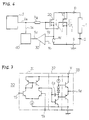
- Figure 2 is a block circuit diagram of an embodiment of the present invention in which a main transistor is an insulated gate bipolar transistor.
- Figure 3 is a block circuit diagram showing another embodiment modified from Fig. 1(a).
- Figure 4 is a block circuit diagram showing another embodiment modified from Fig. 2.
- Fig. 5 is a sectional view of a semiconductor device into which a main transistor and a current detector transistor are incorporated.
- the parts corresponding to those in Fig. 6 are designated by the same reference numerals or symbols, and their explanations are omitted for simplicity.
- the main transistor 10 and the current detector transistor 20 shown in Fig. 1 (a) are built in a semiconductor device in almost the same structure and their load side terminals are commonly connected as a drain terminal D, as shown in the figure similarly as in Fig. 6.
- a major difference between the embodiment of Fig. 1 (a) and the prior art of Fig 6 exists in that the gate potential is separated between the main and the current detector transistors 10 and 20 as shown in Fig. 1 (a).
- the electrostatic capacitance of the gate of the current detector transistor 20 is 1 pF or less, i. e.
- the drive command Ss from the drive circuit 3, which designates ON and OFF for example, is fed to the main transistor 10 as usual through gate resistor Rg and directly, in this embodiment, to the current detector transistor 20.
- a current detecting means Rd is comprised, for example, of a resistor which receives the current i flowing through the current detector transistor 20 and outputs the detection signal Vd indicative of voltage drop across the resistor.
- a gate control means 50 which receives the detection signal Vd is comprised, as illustrated by a single dotted chain line, of a comparator circuit 30 and a control circuit 40.
- the comparator circuit 30 compares the detection signal Vd with the reference voltage Vr and outputs a comparison output Sd.
- a comparator may be used as the comparator circuit 30, it is more preferable to use such an operational amplifier as shown in Fig. 7. In this case, a phase compensation capacitor shown in Fig. 7 is not always necessary.
- a capacitor with a small capacitance of from several to several ten pF may be used without any trouble.
- the same control circuit 40 as that of Fig. 6 may be used which feeds the control signal Sc to the gates of the main transistor 10 and the current detector transistor 20 by superimposing the control signal Sc onto the drive command Ss from the drive circuit 3 as illustrated in Fig. 1 (a).
- the time constant of the gate of the current detector transistor 20 is usually much smaller than that of the main transistor, less than one thousandth of the time constant of the main transistor.
- the time constant ratio shrinks to less than from one several tenth to one several hundredth because of the equivalent resistance of the gate itself and the gate wiring, the small resistance of a resistor connected for adjusting the response of current detection, and the stray capacitance of the wiring. It is effective to adjust the time constant of the gate circuit of the current detector transistor 20 to less than one tenth of that on the side of the main transistor 10 for fully utilizing the effect of the present invention.
- Figure 1 (b) is a graph showing response characteristics of the embodiment of Fig. 1 (a), i. e. change ⁇ l of the current l of the main transistor 10 when the control signal Sc is abruptly changed.
- the abscissa represents the time t and the ordinate represents the current l.
- curve A represents the response according to the present invention
- curve B the response according to the prior art.
- the characteristic curve A of the present invention does not show any oscillation and converges to a constant value in a short time after a small peak has occurred. Since current detection response is quick because of the short time constant of the current detector transistor 20 according to the present invention, it becomes unnecessary to forcibly conduct gate control based on the slow current detection response according to the prior art.
- a main and a current detector transistor 11 and 21 are comprised of insulated gate bipolar transistors. Load side collector terminals C of the transistors 11, 21 are connected in common, and an emitter terminal E of the main transistor 11 is grounded.
- the insulated gate bipolar transistor is especially suitable for large current use. Since the main transistor is comprised of many unit structures, similar to the power MOS transistor, the current detector transistor 21 is easily incorporated with the main transistor 11 by assigning one or two of the unit structures to the current detector transistor 21.
- the gate control means 50 is configured more simply than in the embodiments described above.
- a field effect type control transistor 51 is incorporated into the gate control means 50 and the operation threshold of the gate of the control transistor 51 is utilized as the limit value with which the voltage of the detection signal Vd from the current detecting means Rd is compared.
- the detection signal Vd is fed to the gate of the control transistor 51 to switch on the control transistor 51 when the voltage value of the detection signal Vd exceeds the threshold value of the gate as shown in the figure.
- the gate potential of the main transistor 10 and the gate potential of the current detector transistor 20 are lowered through a resistor 52 when the control transistor 51 is switched on to protect the main transistor from an over current.
- the gate threshold value of the control transistor 51 can satisfactorily be used as the limit value with which the voltage value of the detection signal Vd is compared for over current protection.
- the resistance value of the current detecting means Rd is, though different case by case, preferably set within a range between several ⁇ and 1 k ⁇ when the gate threshold value of the control transistor 51 is 1 V as usual.
- the resistor 52 is incorporated into the gate control means 50 in Fig. 3 for limiting a leakage current which flows via the control transistor 51 when the polarity of the drive command Ss from the drive circuit 3 turns to negative and for adjusting the gain of the control transistor 51 at a not too high value.
- the time constant of the gate circuit of the current detector transistor 20 is adjusted by connecting a gate resistor rg of small resistance value so as to maintain the proportionality of the ratio of current of the current detector transistor 20 to the current of the main transistor 10 as constant as possible even when the load 1 abruptly changes.
- the main transistor 10 and the current detector transistor 20 are shown as the MOS transistors in Fig. 3, the transistors 10, 20 may be insulated gate bipolar transistors. Further, a gate resistor rg may also be employed in the embodiment of Fig. 2 as indicated in the figure.
- the main transistor 11 and the current detector transistor 21 are insulated gate bipolar transistors.
- the main transistor 11 is used as a low side switch connected directly to a power supply 2.
- the gate resistor rg is connected to the current detector transistor 21 also in this embodiment.
- the control transistor 51 is incorporated into the gate control means 50 as in Fig. 3.
- a Zener diode 53 and a diode 54 are used in place of the resistor 52.
- the Zener diode 53 is used for preventing oscillation, which often happens in association with an abrupt change of the gate potential, by setting a minimum potential for the gates of the main and the current detector transistors 11, 21.
- the diode 54 prevents the aforementioned leakage current or a reverse current from flowing to the drive circuit 3 when the drive command Ss turns to negative.
- the electrostatic capacitance of the main power transistor 10 or 11 is typically about 5 nF, the electrostatic capacitance of the small current detector transistor 20 or 21 is less than 1 pF, and the capacitance ratio is from 1000 to 10000 : 1. It has been found by an experiment, in which the gate resistor Rg for the main transistor 10 or 11 was set to 100 ⁇ and the gate resistor rg for the current detector transistor 20 or 21 was varied, that the oscillation prevention function as shown by the curve A in Fig. 1 (b) is obtained with excellent reproducibility in a wide range of the gate resistor rg of from 1 ⁇ to 10 k ⁇ .
- a transistor or a switching element which has an operation threshold on the input side such as a junction type field effect transistor, a bipolar transistor, etc.
- a MOS transistor or an insulated gate bipolar transistor is used for the main transistor 10 or 11 in Figs. from 1 to 4, the present invention is also applicable to all the power semiconductor devices comprised of a semiconductor device having an insulated gate such as a MOS gate type thyristor.
- Figure 5 shows two unit structures for the main transistor 10 on the right hand side of the figure and one unit structure for the current detector transistor 20 on the left hand side.
- a semiconductor base plate 60 is comprised of an n-type semiconductor substrate 61 and an epitaxial layer 62 grown on the semiconductor substrate 61.
- the transistors 10 and 20 with vertical structure are built into the epitaxial layer 62 from the surface side.
- a deep well 63 for each unit structure and a stopper layer 64 between the transistors 10 and 20 with impurity concentration of from 1017 to 1018 atoms/cm3 are simultaneously diffused into the depth of from 4 to 8 ⁇ m from the surface of the epitaxial layer 62.
- a so-called field oxide film of about 1 ⁇ m in thickness is deposited as insulation film 65 on the entire surface of the epitaxial layer 62.
- the field oxide film is etched off leaving a portion between both transistors behind.
- a very thin gate oxide film 66 is then deposited on the surface of the etched-off portion.
- gate 67 is directly formed on the gate oxide film 66 on the side of the main transistor 10.
- an extended portion 67a of the gate 67 is extended from above the gate oxide film 66 over to the insulation film 65.
- the extended portion 67a of the gate 67 is also extended from the edge of the unit structure for the main transistor 10 over to the insulation film 65.
- a p-type well layer 68 and a pair of n-type source layers 69 are built in for each unit structure in a so-called double diffusion structure by ion implantation of p-type and n-type impurities using the gate 67 as a mask and by simultaneous thermal diffusion of the implanted impurities.
- the p-type well layer 68 with impurity concentration of 1017 atoms/cm3 is diffused deeply down to the depth of from 2 to 4 ⁇ m and the n-type source layer 69 with impurity concentration of 1019 atoms/cm3 is diffused to shallow depth.
- interlayer insulation film 70 predetermined portions of which are then opened for windows.
- An aluminum electrode 71 is then deposited to form a source terminal S1 of the main transistor 10 and a source terminal S2 of the current detector transistor 20.
- Electrode film 71 is deposited also on the back surface of the base plate 60 to form a common drain terminal D of the transistors 10, 20.
- Gate terminals 61 and 62 of the transistors 10 and 20 are individually led out from the portions not shown in Fig. 5.
- the current detector resistor Rd and the gate resistor Rg are built in the semiconductor base plate 60 in the from of, for example, so-called diffused resistors.
- the embodiment of Fig. 5 prevents the leakage current by reducing an electric field gradient on the epitaxial layer 62 with the relatively thick insulation film 65 covering the surface of the epitaxial layer 62 and the extended portion 67a of the gate 67 disposed on the insulation film 65.
- the embodiment of Fig. 5 almost completely shuts off the leakage current with the p-type stopper layer 64 in-diffused in the surface portion of the n-type epitaxial layer 62 around the gap between the edges of the extended portions 67 as of the gates of the transistors 10 and 20.
- the stopper layer 64 is preferably biased to the electric potential of the source terminal S1 or S2, among which the electric potential of the source terminal S2 is especially recommended, though the electric potential of the stopper layer 64 may be floated.
- the provision of the stopper layer 64 does not increase processing steps, since the stopper layer 64 is in-diffused simultaneously when the deep well 63 is formed in each unit structure for preventing latch-up.
- the over current protection device is shown for one main transistor 10 or 11.
- the over current protection device of the present invention may be provided for each of plural main transistors or for one representative transistor and a drive circuit 3 in common to the main transistors, since from 4 to 6 main transistors are used in a three-phase or two-phase bridge circuit for a power inverter or for motor drive. Since the integrated circuits into which the over current protection device is incorporated with several main transistors 10 or 11 have been increasing in these days, the structure of Fig. 5 can be effectively applied to these integrated circuits.
- the over current protection device of the present invention is best suited for over current protection of large capacity main transistors having a withstand voltage of from 600 to 2000 V and a rated current of from 10 to several hundreds A.
- the present invention has solved the problem of the prior art based on the finding that oscillation at gate control in over current protections is prevented simply by improving the response of gate control on the side of the current detector transistor.
- the present invention which protects the main transistor from over current by reducing the electrostatic gate capacitance of the current detector transistor by separating the gate of the current detector transistor from the gate of the main transistor, by setting the time constant of the detector transistor gate circuit at a much shorter value than, preferably at less than one tenth of, the time constant of the main transistor gate circuit, by feeding the detection signal obtained by detecting the current flowing through the detector transistor with a current detecting means to the gate control mains, and by controlling the gates of the main and current detector transistors when the detection signal exceeds a predetermined limit value, the following effects are obtained.
Landscapes
- Engineering & Computer Science (AREA)
- Power Engineering (AREA)
- Semiconductor Integrated Circuits (AREA)
- Metal-Oxide And Bipolar Metal-Oxide Semiconductor Integrated Circuits (AREA)
- Insulated Gate Type Field-Effect Transistor (AREA)
- Protection Of Static Devices (AREA)
- Continuous-Control Power Sources That Use Transistors (AREA)
- Power Conversion In General (AREA)
- Amplifiers (AREA)
Applications Claiming Priority (4)
| Application Number | Priority Date | Filing Date | Title |
|---|---|---|---|
| JP24584093 | 1993-10-01 | ||
| JP245840/93 | 1993-10-01 | ||
| JP6041654A JPH07146722A (ja) | 1993-10-01 | 1994-03-14 | トランジスタ用過電流保護装置 |
| JP41654/94 | 1994-03-14 |
Publications (3)
| Publication Number | Publication Date |
|---|---|
| EP0647026A2 true EP0647026A2 (fr) | 1995-04-05 |
| EP0647026A3 EP0647026A3 (fr) | 1996-01-17 |
| EP0647026B1 EP0647026B1 (fr) | 1998-01-14 |
Family
ID=26381306
Family Applications (1)
| Application Number | Title | Priority Date | Filing Date |
|---|---|---|---|
| EP94115435A Expired - Lifetime EP0647026B1 (fr) | 1993-10-01 | 1994-09-30 | Dispositif de protection contre la surintensité pour transistor |
Country Status (4)
| Country | Link |
|---|---|
| US (1) | US5621601A (fr) |
| EP (1) | EP0647026B1 (fr) |
| JP (1) | JPH07146722A (fr) |
| DE (1) | DE69407914T2 (fr) |
Cited By (9)
| Publication number | Priority date | Publication date | Assignee | Title |
|---|---|---|---|---|
| EP0793343A1 (fr) * | 1996-02-29 | 1997-09-03 | Co.Ri.M.Me. Consorzio Per La Ricerca Sulla Microelettronica Nel Mezzogiorno | Circuit programmable avec limitation de courant pour les actuateurs de puissance |
| EP0691687A3 (fr) * | 1994-06-22 | 1997-10-15 | Fuji Electric Co Ltd | Dispositif à semi-conducteur de type MOS vertical |
| DE19854821A1 (de) * | 1998-11-27 | 2000-05-31 | Bosch Gmbh Robert | Schutzschaltung für eine getaktete Halbleiter-Endstufe |
| WO2000069067A1 (fr) * | 1999-05-10 | 2000-11-16 | Tyco Electronics Logistics A.G. | Dispositif de detection de puissance pour amplificateurs de puissance |
| DE10060553A1 (de) * | 2000-12-06 | 2002-06-13 | Daimlerchrysler Rail Systems | Überstrom-Erfassungseinrichtung |
| WO2005027328A1 (fr) * | 2003-09-10 | 2005-03-24 | Toshiba Mitsubishi-Electric Industrial Systems Corporation | Circuit de commande de grille |
| EP1349251A3 (fr) * | 2000-07-24 | 2006-09-13 | Yazaki Corporation | Dispositif de commutation à semiconducteur comportant un FET de puissance à sources multiples fournissant un courant de mesure et permettant un nombre prédéterminé d'essais de reconnexion avant l'arrêt d'urgence |
| GB2427087A (en) * | 2005-06-06 | 2006-12-13 | Avago Technologies General Ip | An output-current-limited driver with improved stability |
| CN105960618A (zh) * | 2014-02-13 | 2016-09-21 | 罗伯特·博世有限公司 | 用于检测电流的电流探测装置和方法 |
Families Citing this family (59)
| Publication number | Priority date | Publication date | Assignee | Title |
|---|---|---|---|---|
| JPH08154022A (ja) * | 1994-11-29 | 1996-06-11 | Nec Corp | 過電流保護回路付き増幅回路 |
| JP3911566B2 (ja) * | 1998-01-27 | 2007-05-09 | 富士電機デバイステクノロジー株式会社 | Mos型半導体装置 |
| JP2982785B2 (ja) * | 1998-04-03 | 1999-11-29 | 富士電機株式会社 | デプレッション型mos半導体素子およびmosパワーic |
| JP3164065B2 (ja) * | 1998-06-24 | 2001-05-08 | 日本電気株式会社 | 半導体装置 |
| US6269011B1 (en) * | 1999-02-14 | 2001-07-31 | Yazaki Corporation | Power supply system having semiconductor active fuse |
| JP2000308340A (ja) * | 1999-02-19 | 2000-11-02 | Yazaki Corp | ヒューズレスdc/dcコンバータ |
| US6653669B2 (en) * | 1999-06-28 | 2003-11-25 | Stmicroelectronics Sa | Device for the adjustment of circuits after packaging |
| US20030054780A1 (en) * | 2000-09-05 | 2003-03-20 | Hitachi, Ltd. | High frequency power amplifying circuit, and mobile communication apparatus using it |
| US6717787B2 (en) | 2001-02-22 | 2004-04-06 | Koninklijke Philips Electronics N.V. | Current sensing IC with resistive sensing |
| TW517422B (en) * | 2001-05-18 | 2003-01-11 | Palmax Technology Co Ltd | Input protection circuit of hand-held electrical apparatus |
| JP2003197913A (ja) * | 2001-12-26 | 2003-07-11 | Nec Electronics Corp | 半導体集積回路 |
| JP3886876B2 (ja) * | 2002-01-17 | 2007-02-28 | 三菱電機株式会社 | 電力用半導体素子の駆動回路 |
| DE10205711A1 (de) * | 2002-02-12 | 2003-08-21 | Infineon Technologies Ag | Verfahren und Vorrichtung zum Erfassen eines Durchbruchs eines Bipolartransistors |
| US6897715B2 (en) * | 2002-05-30 | 2005-05-24 | Analog Devices, Inc. | Multimode voltage regulator |
| US6819165B2 (en) * | 2002-05-30 | 2004-11-16 | Analog Devices, Inc. | Voltage regulator with dynamically boosted bias current |
| AU2002950581A0 (en) * | 2002-08-02 | 2002-09-12 | Wayne Callen | Electrical safety circuit |
| US7372685B2 (en) * | 2003-05-20 | 2008-05-13 | On Semiconductor | Multi-fault protected high side switch with current sense |
| ITMI20040356A1 (it) * | 2004-02-27 | 2004-05-27 | St Microelectronics Srl | Circuito di pilotaggio di una configurazione emitter switching per controllare il livello di saturazione di un transistore di potenza in applicazioni che prevedono correnti di collettoree variabili in un ampio intervallo |
| JP2005260658A (ja) * | 2004-03-12 | 2005-09-22 | Nec Electronics Corp | 半導体装置 |
| US6992523B2 (en) * | 2004-04-27 | 2006-01-31 | Texas Instruments Incorporated | Low voltage current monitoring circuit |
| JP4807768B2 (ja) * | 2004-06-23 | 2011-11-02 | ルネサスエレクトロニクス株式会社 | パワートランジスタ装置及びそれを用いたパワー制御システム |
| JP2006053898A (ja) * | 2004-07-15 | 2006-02-23 | Rohm Co Ltd | 過電流保護回路およびそれを利用した電圧生成回路ならびに電子機器 |
| JP2008537414A (ja) * | 2005-04-18 | 2008-09-11 | フリースケール セミコンダクター インコーポレイテッド | 電力増幅器のための適応保護回路 |
| JP4996203B2 (ja) * | 2006-11-07 | 2012-08-08 | ルネサスエレクトロニクス株式会社 | 電源電圧回路 |
| US7843248B1 (en) * | 2007-11-01 | 2010-11-30 | Intersil Americas Inc. | Analog switch with overcurrent detection |
| CN101582632A (zh) * | 2008-05-12 | 2009-11-18 | 鸿富锦精密工业(深圳)有限公司 | 开关电源及使用该开关电源的用电设备 |
| US7986149B2 (en) * | 2008-08-19 | 2011-07-26 | Infineon Technologies Austria Ag | System and method for adaptive load fault detection |
| WO2010109596A1 (fr) | 2009-03-24 | 2010-09-30 | トヨタ自動車株式会社 | Dispositif à semi-conducteurs |
| EP2261190A1 (fr) | 2009-06-12 | 2010-12-15 | Treibacher Industrie AG | Composition d'émail à base d'yttrium |
| JP5289580B2 (ja) | 2009-10-20 | 2013-09-11 | 三菱電機株式会社 | 半導体装置 |
| JP5430438B2 (ja) * | 2010-02-18 | 2014-02-26 | パナソニック株式会社 | デジタルアンプ |
| JP2011174712A (ja) * | 2010-02-23 | 2011-09-08 | On Semiconductor Trading Ltd | 電流検出回路及び半導体集積回路 |
| JP5724281B2 (ja) | 2010-10-08 | 2015-05-27 | 富士電機株式会社 | パワー半導体デバイスの電流検出回路 |
| JP5170208B2 (ja) | 2010-10-22 | 2013-03-27 | 富士電機株式会社 | パワー半導体デバイスの電流検出回路 |
| US8766375B2 (en) * | 2011-03-21 | 2014-07-01 | International Rectifier Corporation | Composite semiconductor device with active oscillation prevention |
| WO2013005520A1 (fr) | 2011-07-06 | 2013-01-10 | 富士電機株式会社 | Circuit de correction de courant et procédé de correction de courant pour dispositif à semi-conducteur de puissance |
| CN102510046B (zh) * | 2011-11-03 | 2014-11-19 | 宁波沪江电机有限公司 | 一种电机用过流保护装置 |
| JPWO2014097739A1 (ja) | 2012-12-17 | 2017-01-12 | 富士電機株式会社 | 半導体装置 |
| JP5772842B2 (ja) | 2013-01-31 | 2015-09-02 | 株式会社デンソー | 炭化珪素半導体装置 |
| JP2015028969A (ja) * | 2013-07-30 | 2015-02-12 | 本田技研工業株式会社 | 半導体装置 |
| JP6324696B2 (ja) | 2013-10-03 | 2018-05-16 | 三菱重工オートモーティブサーマルシステムズ株式会社 | 負荷駆動装置及びそれを備えた車両用空調装置並びに負荷短絡保護回路 |
| JP2015119521A (ja) * | 2013-12-17 | 2015-06-25 | サンケン電気株式会社 | 半導体装置及びスイッチング回路 |
| JP2015119594A (ja) * | 2013-12-19 | 2015-06-25 | トヨタ自動車株式会社 | 半導体装置の駆動制御装置 |
| JP6510310B2 (ja) | 2014-05-12 | 2019-05-08 | ローム株式会社 | 半導体装置 |
| JP6772328B2 (ja) * | 2014-05-12 | 2020-10-21 | ローム株式会社 | 半導体装置 |
| JP6265099B2 (ja) * | 2014-10-08 | 2018-01-24 | 三菱電機株式会社 | 半導体装置 |
| US10141923B2 (en) * | 2016-08-25 | 2018-11-27 | Toyota Motor Engineering & Manufacturing North America, Inc. | System and method for eliminating gate voltage oscillation in paralleled power semiconductor switches |
| US11082039B2 (en) * | 2017-11-08 | 2021-08-03 | Gan Systems Inc. | GaN transistor with integrated drain voltage sense for fast overcurrent and short circuit protection |
| EP3518421A1 (fr) * | 2018-01-30 | 2019-07-31 | Siemens Aktiengesellschaft | Protection d'un transistor à effet de champ fonctionnant dans le mode de commutation contre un courant de surcharge |
| JP7155534B2 (ja) * | 2018-02-16 | 2022-10-19 | 富士電機株式会社 | 半導体装置 |
| JP2021076463A (ja) * | 2019-11-08 | 2021-05-20 | ルネサスエレクトロニクス株式会社 | 半導体装置 |
| JP7325314B2 (ja) * | 2019-12-12 | 2023-08-14 | 三菱電機株式会社 | 半導体装置 |
| US11309882B2 (en) | 2019-12-20 | 2022-04-19 | Texas Instruments Incorporated | OPAMP overload power limit circuit, system, and a method thereof |
| US11362504B2 (en) * | 2020-07-20 | 2022-06-14 | Analog Devices International Unlimited Company | Over current sensing scheme for switch applications |
| JP7572202B2 (ja) * | 2020-10-12 | 2024-10-23 | ローム株式会社 | 半導体装置、絶縁型スイッチング電源 |
| US11736100B2 (en) * | 2021-05-05 | 2023-08-22 | Gan Systems Inc. | Active gate voltage control circuit for burst mode and protection mode operation of power switching transistors |
| JP7686521B2 (ja) * | 2021-09-24 | 2025-06-02 | 三菱電機株式会社 | 半導体装置 |
| JPWO2023084948A1 (fr) * | 2021-11-12 | 2023-05-19 | ||
| US12130311B2 (en) * | 2022-12-14 | 2024-10-29 | Infineon Technologies Austria Ag | Current sense circuitry |
Family Cites Families (9)
| Publication number | Priority date | Publication date | Assignee | Title |
|---|---|---|---|---|
| US4783690A (en) * | 1983-09-06 | 1988-11-08 | General Electric Company | Power semiconductor device with main current section and emulation current section |
| US4893158A (en) * | 1987-06-22 | 1990-01-09 | Nissan Motor Co., Ltd. | MOSFET device |
| US4924344A (en) * | 1989-02-27 | 1990-05-08 | Teledyne Industries, Inc. | Circuitry for protection against electromotively-induced voltage transients in solid state relay circuits |
| US5184272A (en) * | 1989-03-31 | 1993-02-02 | Hitachi, Ltd. | High-side switch with overcurrent protecting circuit |
| JPH02266712A (ja) * | 1989-04-07 | 1990-10-31 | Fuji Electric Co Ltd | 半導体装置 |
| GB2237462A (en) * | 1989-10-23 | 1991-05-01 | Philips Nv | Overload protection drive circuit for a power transistor |
| US5023692A (en) * | 1989-12-07 | 1991-06-11 | Harris Semiconductor Patents, Inc. | Power MOSFET transistor circuit |
| JP2876694B2 (ja) * | 1990-03-20 | 1999-03-31 | 富士電機株式会社 | 電流検出端子を備えたmos型半導体装置 |
| EP0615342A3 (fr) * | 1993-03-10 | 1995-03-22 | Fuji Electric Co Ltd | Dispositif semi-conducteur. |
-
1994
- 1994-03-14 JP JP6041654A patent/JPH07146722A/ja active Pending
- 1994-09-28 US US08/314,320 patent/US5621601A/en not_active Expired - Lifetime
- 1994-09-30 EP EP94115435A patent/EP0647026B1/fr not_active Expired - Lifetime
- 1994-09-30 DE DE69407914T patent/DE69407914T2/de not_active Expired - Lifetime
Cited By (18)
| Publication number | Priority date | Publication date | Assignee | Title |
|---|---|---|---|---|
| EP0691687A3 (fr) * | 1994-06-22 | 1997-10-15 | Fuji Electric Co Ltd | Dispositif à semi-conducteur de type MOS vertical |
| EP1209745A3 (fr) * | 1994-06-22 | 2005-06-29 | Fuji Electric Co. Ltd. | Dispositif semiconducteur MOS vertical |
| US5804956A (en) * | 1996-02-29 | 1998-09-08 | Co.Ri.M.Me.-Consorzio Per La Ricerca Sulla Microelettronica Nel Messogiorno | Current limitation programmable circuit for smart power actuators |
| EP0793343A1 (fr) * | 1996-02-29 | 1997-09-03 | Co.Ri.M.Me. Consorzio Per La Ricerca Sulla Microelettronica Nel Mezzogiorno | Circuit programmable avec limitation de courant pour les actuateurs de puissance |
| USRE38657E1 (en) * | 1996-02-29 | 2004-11-23 | Stmicroelectronics, Srl | Current limitation programmable circuit for smart power actuators |
| DE19854821B4 (de) * | 1998-11-27 | 2004-07-29 | Robert Bosch Gmbh | Schutzschaltung für eine getaktete Halbleiter-Endstufe |
| DE19854821A1 (de) * | 1998-11-27 | 2000-05-31 | Bosch Gmbh Robert | Schutzschaltung für eine getaktete Halbleiter-Endstufe |
| WO2000069067A1 (fr) * | 1999-05-10 | 2000-11-16 | Tyco Electronics Logistics A.G. | Dispositif de detection de puissance pour amplificateurs de puissance |
| EP1349251A3 (fr) * | 2000-07-24 | 2006-09-13 | Yazaki Corporation | Dispositif de commutation à semiconducteur comportant un FET de puissance à sources multiples fournissant un courant de mesure et permettant un nombre prédéterminé d'essais de reconnexion avant l'arrêt d'urgence |
| EP1213827A3 (fr) * | 2000-12-06 | 2004-06-16 | Bombardier Transportation GmbH | Dispositif détecteur de surintensité de courant |
| DE10060553A1 (de) * | 2000-12-06 | 2002-06-13 | Daimlerchrysler Rail Systems | Überstrom-Erfassungseinrichtung |
| WO2005027328A1 (fr) * | 2003-09-10 | 2005-03-24 | Toshiba Mitsubishi-Electric Industrial Systems Corporation | Circuit de commande de grille |
| US7570102B2 (en) | 2003-09-10 | 2009-08-04 | Toshiba Mitsubishi - Electric Industrial Systems Corporation | Gate driving circuit for driving a gate electrode of an electric power switching element with simple structure |
| GB2427087A (en) * | 2005-06-06 | 2006-12-13 | Avago Technologies General Ip | An output-current-limited driver with improved stability |
| US7221227B2 (en) | 2005-06-06 | 2007-05-22 | Avago Technologies Ecbu Ip (Singapore) Pte. Ltd. | Methods and apparatus for reducing output current oscillations of a driver provided with circuitry that senses and responds to excessive current draws of an output stage of the driver |
| CN105960618A (zh) * | 2014-02-13 | 2016-09-21 | 罗伯特·博世有限公司 | 用于检测电流的电流探测装置和方法 |
| US10013008B2 (en) | 2014-02-13 | 2018-07-03 | Robert Bosch Gmbh | Current detection device and method for sensing an electrical current |
| CN105960618B (zh) * | 2014-02-13 | 2020-09-01 | 罗伯特·博世有限公司 | 用于检测电流的电流探测装置和方法 |
Also Published As
| Publication number | Publication date |
|---|---|
| EP0647026A3 (fr) | 1996-01-17 |
| DE69407914D1 (de) | 1998-02-19 |
| DE69407914T2 (de) | 1998-06-10 |
| JPH07146722A (ja) | 1995-06-06 |
| EP0647026B1 (fr) | 1998-01-14 |
| US5621601A (en) | 1997-04-15 |
Similar Documents
| Publication | Publication Date | Title |
|---|---|---|
| EP0647026B1 (fr) | Dispositif de protection contre la surintensité pour transistor | |
| US5557128A (en) | Insulated-gate type bipolar transistor | |
| US4994904A (en) | MOSFET having drain voltage detection function | |
| US5796290A (en) | Temperature detection method and circuit using MOSFET | |
| US5610425A (en) | Input/output electrostatic discharge protection circuit for an integrated circuit | |
| US5465190A (en) | Circuit and method for protecting power components against forward overvoltages | |
| US5061863A (en) | Transistor provided with a current detecting function | |
| KR100276414B1 (ko) | 절연 게이트형 반도체 장치 | |
| EP0706265B1 (fr) | Circuit détecteur de courant | |
| EP0733283B1 (fr) | Commutateur protege | |
| US5115369A (en) | Avalanche stress protected semiconductor device having variable input impedance | |
| US4562454A (en) | Electronic fuse for semiconductor devices | |
| US5909135A (en) | High-side MOSFET gate protection shunt circuit | |
| EP0523800B1 (fr) | Commutateur semi-conducteur protégé contre les surtensions | |
| US4489340A (en) | PNPN Light sensitive semiconductor switch with phototransistor connected across inner base regions | |
| US4514646A (en) | Semiconductor integrated circuit device including a protective resistor arrangement for output transistors | |
| US6441679B1 (en) | Semiconductor active fuse operating at higher supply voltage employing current oscillation | |
| US5559355A (en) | Vertical MOS semiconductor device | |
| US6248616B1 (en) | Method for suppressing parasitic effects in a junction-isolation integrated circuit | |
| US5652540A (en) | Current sensing circuit having at least one sense cell | |
| JP4256476B2 (ja) | 短絡検出器を有するパワーデバイス | |
| US5027251A (en) | MOSFET including current mirror FET therein | |
| EP0632501B1 (fr) | Dispositif semi-conducteur comprenant des moyens de protection | |
| DE102017002573B4 (de) | Überspannungsschutz | |
| US5559347A (en) | Insulated gate-type bipolar transistor |
Legal Events
| Date | Code | Title | Description |
|---|---|---|---|
| PUAI | Public reference made under article 153(3) epc to a published international application that has entered the european phase |
Free format text: ORIGINAL CODE: 0009012 |
|
| AK | Designated contracting states |
Kind code of ref document: A2 Designated state(s): DE FR GB IT NL |
|
| PUAL | Search report despatched |
Free format text: ORIGINAL CODE: 0009013 |
|
| AK | Designated contracting states |
Kind code of ref document: A3 Designated state(s): DE FR GB IT NL |
|
| 17P | Request for examination filed |
Effective date: 19960104 |
|
| 17Q | First examination report despatched |
Effective date: 19960315 |
|
| GRAG | Despatch of communication of intention to grant |
Free format text: ORIGINAL CODE: EPIDOS AGRA |
|
| GRAH | Despatch of communication of intention to grant a patent |
Free format text: ORIGINAL CODE: EPIDOS IGRA |
|
| GRAH | Despatch of communication of intention to grant a patent |
Free format text: ORIGINAL CODE: EPIDOS IGRA |
|
| GRAA | (expected) grant |
Free format text: ORIGINAL CODE: 0009210 |
|
| AK | Designated contracting states |
Kind code of ref document: B1 Designated state(s): DE FR GB IT NL |
|
| PG25 | Lapsed in a contracting state [announced via postgrant information from national office to epo] |
Ref country code: FR Free format text: LAPSE BECAUSE OF FAILURE TO SUBMIT A TRANSLATION OF THE DESCRIPTION OR TO PAY THE FEE WITHIN THE PRESCRIBED TIME-LIMIT Effective date: 19980114 |
|
| ITF | It: translation for a ep patent filed | ||
| REF | Corresponds to: |
Ref document number: 69407914 Country of ref document: DE Date of ref document: 19980219 |
|
| EN | Fr: translation not filed | ||
| PLBE | No opposition filed within time limit |
Free format text: ORIGINAL CODE: 0009261 |
|
| STAA | Information on the status of an ep patent application or granted ep patent |
Free format text: STATUS: NO OPPOSITION FILED WITHIN TIME LIMIT |
|
| 26N | No opposition filed | ||
| REG | Reference to a national code |
Ref country code: GB Ref legal event code: IF02 |
|
| REG | Reference to a national code |
Ref country code: GB Ref legal event code: 746 Effective date: 20080801 |
|
| PGFP | Annual fee paid to national office [announced via postgrant information from national office to epo] |
Ref country code: NL Payment date: 20080915 Year of fee payment: 15 Ref country code: IT Payment date: 20080926 Year of fee payment: 15 |
|
| PGFP | Annual fee paid to national office [announced via postgrant information from national office to epo] |
Ref country code: GB Payment date: 20081001 Year of fee payment: 15 |
|
| REG | Reference to a national code |
Ref country code: NL Ref legal event code: V1 Effective date: 20100401 |
|
| GBPC | Gb: european patent ceased through non-payment of renewal fee |
Effective date: 20090930 |
|
| PG25 | Lapsed in a contracting state [announced via postgrant information from national office to epo] |
Ref country code: NL Free format text: LAPSE BECAUSE OF NON-PAYMENT OF DUE FEES Effective date: 20100401 |
|
| PG25 | Lapsed in a contracting state [announced via postgrant information from national office to epo] |
Ref country code: GB Free format text: LAPSE BECAUSE OF NON-PAYMENT OF DUE FEES Effective date: 20090930 |
|
| PG25 | Lapsed in a contracting state [announced via postgrant information from national office to epo] |
Ref country code: IT Free format text: LAPSE BECAUSE OF NON-PAYMENT OF DUE FEES Effective date: 20090930 |
|
| REG | Reference to a national code |
Ref country code: DE Ref legal event code: R082 Ref document number: 69407914 Country of ref document: DE Representative=s name: HOFFMANN, ECKART, DIPL.-ING., DE Effective date: 20110826 Ref country code: DE Ref legal event code: R081 Ref document number: 69407914 Country of ref document: DE Owner name: FUJI ELECTRIC CO., LTD., KAWASAKI-SHI, JP Free format text: FORMER OWNER: FUJI ELECTRIC SYSTEMS CO., LTD., TOKYO/TOKIO, JP Effective date: 20110826 |
|
| PGFP | Annual fee paid to national office [announced via postgrant information from national office to epo] |
Ref country code: DE Payment date: 20130925 Year of fee payment: 20 |
|
| REG | Reference to a national code |
Ref country code: DE Ref legal event code: R071 Ref document number: 69407914 Country of ref document: DE |