EP0651399B1 - Durchsichtige Leiter enthaltend Gallium-Indium-Oxide - Google Patents
Durchsichtige Leiter enthaltend Gallium-Indium-Oxide Download PDFInfo
- Publication number
- EP0651399B1 EP0651399B1 EP94307654A EP94307654A EP0651399B1 EP 0651399 B1 EP0651399 B1 EP 0651399B1 EP 94307654 A EP94307654 A EP 94307654A EP 94307654 A EP94307654 A EP 94307654A EP 0651399 B1 EP0651399 B1 EP 0651399B1
- Authority
- EP
- European Patent Office
- Prior art keywords
- aliovalent
- composition
- gaino
- oxide
- matter
- Prior art date
- Legal status (The legal status is an assumption and is not a legal conclusion. Google has not performed a legal analysis and makes no representation as to the accuracy of the status listed.)
- Expired - Lifetime
Links
- 239000004020 conductor Substances 0.000 title claims description 11
- 229910003437 indium oxide Inorganic materials 0.000 title description 5
- 239000000463 material Substances 0.000 claims description 22
- 239000000203 mixture Substances 0.000 claims description 11
- 239000002019 doping agent Substances 0.000 claims description 6
- 239000010936 titanium Substances 0.000 claims description 4
- ATJFFYVFTNAWJD-UHFFFAOYSA-N Tin Chemical compound [Sn] ATJFFYVFTNAWJD-UHFFFAOYSA-N 0.000 claims description 2
- 229910052758 niobium Inorganic materials 0.000 claims description 2
- 229910052718 tin Inorganic materials 0.000 claims description 2
- 229910052719 titanium Inorganic materials 0.000 claims description 2
- 229910005264 GaInO3 Inorganic materials 0.000 claims 2
- XUIMIQQOPSSXEZ-UHFFFAOYSA-N Silicon Chemical compound [Si] XUIMIQQOPSSXEZ-UHFFFAOYSA-N 0.000 claims 1
- RTAQQCXQSZGOHL-UHFFFAOYSA-N Titanium Chemical compound [Ti] RTAQQCXQSZGOHL-UHFFFAOYSA-N 0.000 claims 1
- 229910052732 germanium Inorganic materials 0.000 claims 1
- GNPVGFCGXDBREM-UHFFFAOYSA-N germanium atom Chemical compound [Ge] GNPVGFCGXDBREM-UHFFFAOYSA-N 0.000 claims 1
- 239000010955 niobium Substances 0.000 claims 1
- GUCVJGMIXFAOAE-UHFFFAOYSA-N niobium atom Chemical compound [Nb] GUCVJGMIXFAOAE-UHFFFAOYSA-N 0.000 claims 1
- 229910052710 silicon Inorganic materials 0.000 claims 1
- 239000010703 silicon Substances 0.000 claims 1
- 239000008188 pellet Substances 0.000 description 15
- QZQVBEXLDFYHSR-UHFFFAOYSA-N gallium(III) oxide Inorganic materials O=[Ga]O[Ga]=O QZQVBEXLDFYHSR-UHFFFAOYSA-N 0.000 description 13
- 239000000758 substrate Substances 0.000 description 13
- PJXISJQVUVHSOJ-UHFFFAOYSA-N indium(iii) oxide Chemical compound [O-2].[O-2].[O-2].[In+3].[In+3] PJXISJQVUVHSOJ-UHFFFAOYSA-N 0.000 description 12
- XOLBLPGZBRYERU-UHFFFAOYSA-N tin dioxide Chemical compound O=[Sn]=O XOLBLPGZBRYERU-UHFFFAOYSA-N 0.000 description 12
- 238000000576 coating method Methods 0.000 description 10
- 239000011521 glass Substances 0.000 description 9
- 239000010408 film Substances 0.000 description 7
- 238000012545 processing Methods 0.000 description 7
- VYPSYNLAJGMNEJ-UHFFFAOYSA-N Silicium dioxide Chemical compound O=[Si]=O VYPSYNLAJGMNEJ-UHFFFAOYSA-N 0.000 description 6
- GWEVSGVZZGPLCZ-UHFFFAOYSA-N Titan oxide Chemical compound O=[Ti]=O GWEVSGVZZGPLCZ-UHFFFAOYSA-N 0.000 description 6
- YBMRDBCBODYGJE-UHFFFAOYSA-N germanium dioxide Chemical compound O=[Ge]=O YBMRDBCBODYGJE-UHFFFAOYSA-N 0.000 description 6
- 238000010304 firing Methods 0.000 description 5
- 239000000843 powder Substances 0.000 description 5
- 238000011282 treatment Methods 0.000 description 5
- 238000002474 experimental method Methods 0.000 description 4
- 238000010438 heat treatment Methods 0.000 description 4
- 239000001257 hydrogen Substances 0.000 description 4
- 229910052739 hydrogen Inorganic materials 0.000 description 4
- TWNQGVIAIRXVLR-UHFFFAOYSA-N oxo(oxoalumanyloxy)alumane Chemical compound O=[Al]O[Al]=O TWNQGVIAIRXVLR-UHFFFAOYSA-N 0.000 description 4
- 239000004065 semiconductor Substances 0.000 description 4
- 238000004544 sputter deposition Methods 0.000 description 4
- 238000010521 absorption reaction Methods 0.000 description 3
- 125000004429 atom Chemical group 0.000 description 3
- 239000011248 coating agent Substances 0.000 description 3
- 238000000151 deposition Methods 0.000 description 3
- 230000008021 deposition Effects 0.000 description 3
- AMGQUBHHOARCQH-UHFFFAOYSA-N indium;oxotin Chemical compound [In].[Sn]=O AMGQUBHHOARCQH-UHFFFAOYSA-N 0.000 description 3
- 238000000034 method Methods 0.000 description 3
- UFHFLCQGNIYNRP-UHFFFAOYSA-N Hydrogen Chemical compound [H][H] UFHFLCQGNIYNRP-UHFFFAOYSA-N 0.000 description 2
- QVGXLLKOCUKJST-UHFFFAOYSA-N atomic oxygen Chemical compound [O] QVGXLLKOCUKJST-UHFFFAOYSA-N 0.000 description 2
- 239000000919 ceramic Substances 0.000 description 2
- 238000001816 cooling Methods 0.000 description 2
- 239000013078 crystal Substances 0.000 description 2
- AJNVQOSZGJRYEI-UHFFFAOYSA-N digallium;oxygen(2-) Chemical compound [O-2].[O-2].[O-2].[Ga+3].[Ga+3] AJNVQOSZGJRYEI-UHFFFAOYSA-N 0.000 description 2
- 230000008020 evaporation Effects 0.000 description 2
- 238000001704 evaporation Methods 0.000 description 2
- 238000000227 grinding Methods 0.000 description 2
- 238000000608 laser ablation Methods 0.000 description 2
- 229910052751 metal Inorganic materials 0.000 description 2
- 239000002184 metal Substances 0.000 description 2
- 239000001301 oxygen Substances 0.000 description 2
- 229910052760 oxygen Inorganic materials 0.000 description 2
- BASFCYQUMIYNBI-UHFFFAOYSA-N platinum Chemical compound [Pt] BASFCYQUMIYNBI-UHFFFAOYSA-N 0.000 description 2
- 239000000377 silicon dioxide Substances 0.000 description 2
- 229910001887 tin oxide Inorganic materials 0.000 description 2
- 238000001429 visible spectrum Methods 0.000 description 2
- BQCADISMDOOEFD-UHFFFAOYSA-N Silver Chemical compound [Ag] BQCADISMDOOEFD-UHFFFAOYSA-N 0.000 description 1
- 229910000831 Steel Inorganic materials 0.000 description 1
- VVTSZOCINPYFDP-UHFFFAOYSA-N [O].[Ar] Chemical compound [O].[Ar] VVTSZOCINPYFDP-UHFFFAOYSA-N 0.000 description 1
- 238000000862 absorption spectrum Methods 0.000 description 1
- 238000003491 array Methods 0.000 description 1
- 230000005540 biological transmission Effects 0.000 description 1
- BEQNOZDXPONEMR-UHFFFAOYSA-N cadmium;oxotin Chemical compound [Cd].[Sn]=O BEQNOZDXPONEMR-UHFFFAOYSA-N 0.000 description 1
- 229910052681 coesite Inorganic materials 0.000 description 1
- 150000001875 compounds Chemical class 0.000 description 1
- 229910052906 cristobalite Inorganic materials 0.000 description 1
- 230000001419 dependent effect Effects 0.000 description 1
- 238000011161 development Methods 0.000 description 1
- 230000001747 exhibiting effect Effects 0.000 description 1
- 239000005350 fused silica glass Substances 0.000 description 1
- 229910001195 gallium oxide Inorganic materials 0.000 description 1
- 239000007789 gas Substances 0.000 description 1
- PCHJSUWPFVWCPO-UHFFFAOYSA-N gold Chemical compound [Au] PCHJSUWPFVWCPO-UHFFFAOYSA-N 0.000 description 1
- 229910052737 gold Inorganic materials 0.000 description 1
- 239000010931 gold Substances 0.000 description 1
- 239000004973 liquid crystal related substance Substances 0.000 description 1
- 238000001755 magnetron sputter deposition Methods 0.000 description 1
- 238000002844 melting Methods 0.000 description 1
- 230000008018 melting Effects 0.000 description 1
- 239000011812 mixed powder Substances 0.000 description 1
- 238000002156 mixing Methods 0.000 description 1
- 239000004570 mortar (masonry) Substances 0.000 description 1
- 230000003287 optical effect Effects 0.000 description 1
- 125000004430 oxygen atom Chemical group O* 0.000 description 1
- 239000002245 particle Substances 0.000 description 1
- 239000004033 plastic Substances 0.000 description 1
- 229910052697 platinum Inorganic materials 0.000 description 1
- 238000000634 powder X-ray diffraction Methods 0.000 description 1
- 238000002360 preparation method Methods 0.000 description 1
- 238000004549 pulsed laser deposition Methods 0.000 description 1
- 230000009257 reactivity Effects 0.000 description 1
- 235000012239 silicon dioxide Nutrition 0.000 description 1
- 229910052709 silver Inorganic materials 0.000 description 1
- 239000004332 silver Substances 0.000 description 1
- 239000007858 starting material Substances 0.000 description 1
- 239000010959 steel Substances 0.000 description 1
- 229910052682 stishovite Inorganic materials 0.000 description 1
- 239000010409 thin film Substances 0.000 description 1
- 239000004408 titanium dioxide Substances 0.000 description 1
- 238000000411 transmission spectrum Methods 0.000 description 1
- 229910052905 tridymite Inorganic materials 0.000 description 1
- 230000000007 visual effect Effects 0.000 description 1
- YVTHLONGBIQYBO-UHFFFAOYSA-N zinc indium(3+) oxygen(2-) Chemical compound [O--].[Zn++].[In+3] YVTHLONGBIQYBO-UHFFFAOYSA-N 0.000 description 1
Images
Classifications
-
- H—ELECTRICITY
- H01—ELECTRIC ELEMENTS
- H01B—CABLES; CONDUCTORS; INSULATORS; SELECTION OF MATERIALS FOR THEIR CONDUCTIVE, INSULATING OR DIELECTRIC PROPERTIES
- H01B1/00—Conductors or conductive bodies characterised by the conductive materials; Selection of materials as conductors
- H01B1/06—Conductors or conductive bodies characterised by the conductive materials; Selection of materials as conductors mainly consisting of other non-metallic substances
- H01B1/08—Conductors or conductive bodies characterised by the conductive materials; Selection of materials as conductors mainly consisting of other non-metallic substances oxides
-
- G—PHYSICS
- G02—OPTICS
- G02F—OPTICAL DEVICES OR ARRANGEMENTS FOR THE CONTROL OF LIGHT BY MODIFICATION OF THE OPTICAL PROPERTIES OF THE MEDIA OF THE ELEMENTS INVOLVED THEREIN; NON-LINEAR OPTICS; FREQUENCY-CHANGING OF LIGHT; OPTICAL LOGIC ELEMENTS; OPTICAL ANALOGUE/DIGITAL CONVERTERS
- G02F1/00—Devices or arrangements for the control of the intensity, colour, phase, polarisation or direction of light arriving from an independent light source, e.g. switching, gating or modulating; Non-linear optics
- G02F1/01—Devices or arrangements for the control of the intensity, colour, phase, polarisation or direction of light arriving from an independent light source, e.g. switching, gating or modulating; Non-linear optics for the control of the intensity, phase, polarisation or colour
- G02F1/13—Devices or arrangements for the control of the intensity, colour, phase, polarisation or direction of light arriving from an independent light source, e.g. switching, gating or modulating; Non-linear optics for the control of the intensity, phase, polarisation or colour based on liquid crystals, e.g. single liquid crystal display cells
- G02F1/133—Constructional arrangements; Operation of liquid crystal cells; Circuit arrangements
- G02F1/1333—Constructional arrangements; Manufacturing methods
- G02F1/1343—Electrodes
- G02F1/13439—Electrodes characterised by their electrical, optical, physical properties; materials therefor; method of making
-
- H—ELECTRICITY
- H10—SEMICONDUCTOR DEVICES; ELECTRIC SOLID-STATE DEVICES NOT OTHERWISE PROVIDED FOR
- H10F—INORGANIC SEMICONDUCTOR DEVICES SENSITIVE TO INFRARED RADIATION, LIGHT, ELECTROMAGNETIC RADIATION OF SHORTER WAVELENGTH OR CORPUSCULAR RADIATION
- H10F77/00—Constructional details of devices covered by this subclass
- H10F77/20—Electrodes
- H10F77/244—Electrodes made of transparent conductive layers, e.g. transparent conductive oxide [TCO] layers
Definitions
- This invention relates to conducting materials and, in particular, to conducting materials comprising gallium-indium-oxide, GaInO 3 , doped to exhibit electrical conductivity in a transparent state.
- Transparent conductive materials are important components in visual communications devices and useful in a variety of other applications.
- arrays of transparent electrodes define the display segments or even pixels to be activated.
- transparent conductors can be used as antistatic coatings on instrument panels, heating elements on aircraft windows, and electrodes on solar cells. Such materials are also useful as heat retaining and ultraviolet light-rejecting coatings on windows.
- ITO indium tin oxide
- ITO coatings typically have an index of about 2.0 whereas typical glasses have an index of about 1.5.
- the result is reflection loss at the ITO/glass interface, reducing the amount of transmitted light. Accordingly, there is a need for transparent conductive material having enhanced transparency and better index matching with glass.
- aliovalently doped gallium-indium-oxide can achieve electrical conductivity comparable to wide band-gap semiconductors presently in use while exhibiting enhanced transparency and improved index matching.
- the material can be doped to resistivity of less than 10 milliohm-cm by small quantities of aliovalent dopants, such as tetravalent atoms. It has a refractive index of about 1.6 and can be deposited on glass substrates in polycrystalline films.
- GaInO 3 is enhanced by small quantities of aliovalent dopants M in GaIn 1-x M x O 3 .
- An aliovalent dopant is a dopant which has a valence different from the other atoms in the host compound).
- the aliovalent dopant should have a valence greater than 3 and preferably is tetravalent.
- GaIn 0.94 Sn 0.06 O 3 for example, provided resistivity of 2 milliohm-cm in a 0.6 micrometer thick film.
- Ga 1-x Ge x InO 3 0.005 ⁇ x ⁇ 0.12
- GaIn 1-x Ge x O 3 also gives good transparency and conductivity.
- Doping with Ti or Nb provided enhanced conductivity, but it was two orders of magnitude lower than the conductivity produced by tin.
- Doping with Si yielded similar results when Si was substituted for Ga.
- a series of experiments with Ga 1+x In 1-x-y Sn y O 3 and Ga 1+x-y Ge y In 1-x O 3 for 0.25 ⁇ x and .005 ⁇ y ⁇ .12 also showed conductivity and good transparency.
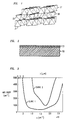
- FIG. 1 is a polyhedral representation of the crystal structure of GaInO 3 .
- the metal atoms are in the centers of the polyhedra, and the oxygen atoms are at the corners.
- the tetrahedra 20 represent GaO 4 and the octahedra 21 represent InO 6 .
- GaInO 3 exhibits a ⁇ gallia crystal structure similar to one of the forms of Ga 2 O 3 .
- Ga 2 O 3 analog Ga is present in two crystallographic metal sites: a four coordinate site and a six coordinate site.
- GaInO 3 Ga is on the four coordinate site, and In is on the six coordinate site.
- GaInO 3 can be mixed with Ga 2 O 3 in a continuous range.
- GaInO 3 is conductively doped if it is doped to a resistivity of 10 milliohm-cm or less.
- Powdered gallium oxide, Ga 2 O 3 , indium oxide, In 2 O 3 , and tin oxide, SnO 2 are weighed out to yield the appropriate mole ratios for GaIn 1-x Sn x O 3 .
- a 5-gram total weight sample of GaIn .94 Sn .06 O 3 2.0090 grams of Ga 2 O 3 , 2.7972 grams of In 2 O 3 and 0.1938 grams of SnO 2 are used.
- the powders are mixed together and ground together in a mechanical mortar and pestle for a minimum of five minutes to insure good mixing and contact of powder particles.
- the mixed powders are transferred into high density aluminum oxide crucibles with cover and heated in air for an initial period of 12-15 hours at temperatures between 1100 and 1200°C.
- the resulting powders are then ground mechanically again, re-introduced into the covered aluminum oxide crucibles, and heated for a period of 12-15 hours at 1300°C in air.
- pellets are pressed in a standard steel dye (typically to a load of 3000 pounds for a half-inch diameter pellet). The pellets are then heated again at 1300°C in air for a period of up to 60 hours.
- Pellets are typically placed on powder of their own composition inside the covered aluminum oxide crucibles for the pellet firing step.
- the pellets are cooled after this heating step at the natural cooling rate of the furnace, which in our case results in reaching 300°C in approximately three hours, at which point the pellets are removed from the furnace.
- the resulting pellets are typically single phase materials (to the detectability limits of standard powder x-ray diffraction) of the GaInO 3 structure type.
- Air is selected as an ambient for the initial processing steps because of its convenience. Covers are placed over the crucibles as a precaution to prevent evaporation of the oxides, but we have not observed evaporation under the conditions described.
- the first air firing need not necessarily be in the 1100-1200°C range, but we select an initial low temperature to reduce the possibility of metastable melting.
- the final heating temperature of 1300°C in air gave more satisfactory conductivities, in one set of experiments, than did a 1400°C air treatment.
- the times and temperatures of these treatments are expected to be dependent on the reactivities of the starting materials and the efficiencies of the grinding operations. Shorter times can be expected to give equally satisfactory results, for example, in the preparation of ceramic targets for sputtering or laser ablation.
- the material after air firings are not in their optimally conducting state.
- a further treatment is advantageous to improve the conductivity.
- a heating of duration 10-12 hours in flowing N 2 (approximately 100 cc/min, N 2 typically approximately 50-100 ppm O 2 ) in a ceramic tube furnace at 1200°C is employed, again with the pellets allowed to cool at the natural furnace cooling rate. Covered aluminum oxide crucibles and a powder bed for the pellets need not necessarily be employed for this step.
- the pellets emerge from the N 2 treatment with good electrical conductivity and a light grey-to-white color.
- GaIn 1-x Ti x O 3 Processing conditions as described in Example 1, with Ga 2 O 3 ,In 2 O 3 and TiO 2 (titanium dioxide) mixed in appropriate mole ratios to yield GaIn 1-x Ti x O 3 .
- GaIn .96 Ti .04 O 3 in a 5 gram batch, 2.0358 grams of Ga 2 O 3 , 0.0694 grams of TiO 2 , and 2.8948 grams of In 2 O 3 are employed.
- pellets of undoped GaInO 3 after firing can be heated in a reducing ambient (e.g. nitrogen-hydrogen (15 mole percent hydrogen) at 600-650°C).
- a reducing ambient e.g. nitrogen-hydrogen (15 mole percent hydrogen) at 600-650°C.
- nitrogen-hydrogen 15 mole percent hydrogen
- FIG. 2 is a schematic cross section of a substrate 30, such as a transparent glass, coated with a thin layer 31 comprising conductively doped GaInO 3 .
- the coating is in the form of a thin continuous polycrystalline layer having a thickness typically in the range 0.1 ⁇ m to 1 ⁇ m.
- the method for coating a substrate 30 can be understood by considering the following examples.
- a pressed pellet of Ga 0.9 Ge 0.1 InO 3 was placed in the target holder of a pulsed laser deposition vacuum chamber and a vitreous quartz substrate was mounted onto a heatable substrate holder facing the target and positioned about 8 cm from the target.
- the chamber was evacuated to a base pressure of 1-10x10 -7 Torr and 1 m Torr of oxygen was bled into the chamber.
- the substrate was heated to 250°C, and then the target was bombarded by pulses from a KrF excimer laser operating at 248 nm with a pulse repetition rate at 10 Hz.
- the energy density of the laser on target was 1-4 J/cm 2 .
- the deposition rate was 1000-1500 angstroms per hour. After growth of several thousand angstroms, the chamber was again evacuated and the substrate was permitted to cool to room temperature. The films subsequently removed from the chamber were transparent to the eye with good electrical conductivity.
- a pressed pellet of Ga 1-x Sn x InO 3 was placed in the target holder of a dc magnetron sputter deposition chamber.
- Corning glass and fused silica substrates were placed in proximity to the target in two configurations: (1) on-axis geometry directly underneath the target and (2) off-axis geometry outside the plasma plume, approximately 0.5-2.0 cm from the edge of the sputtering gun.
- the chamber was evacuated, and a sputtering gas consisting of an argon-oxygen mixture (15-1 ratio) at 4-20 m Torr was introduced.
- the substrate was heated to 250°C - 500°C.
- the target was then impacted by the sputter gun (a US 1'' magnetron source) operating at a dc voltage of 350V, a current of 0.78A, and a power level of 25 Watts.
- the growth rate was about 1.3 ⁇ m per hour in the on-axis geometry and .25 to 0.5 ⁇ m per hour in the off-axis geometry.
- the films had resistivity of about 2.5 milliohm-cm in a 0.4 micrometer thick film and exhibited transmission superior to indium tin oxide in the green and blue regions.
- FIG. 3 is a graphical illustration of the absorption spectrum of conductively doped GaInO 3 (curve 1) in comparison with that of conventional ITO (curve 2). As can be seen, the GalnO 3 film exhibits uniformly small absorption across the visible spectrum.
Landscapes
- Physics & Mathematics (AREA)
- Nonlinear Science (AREA)
- Mathematical Physics (AREA)
- Chemical & Material Sciences (AREA)
- Crystallography & Structural Chemistry (AREA)
- General Physics & Mathematics (AREA)
- Optics & Photonics (AREA)
- Non-Insulated Conductors (AREA)
- Conductive Materials (AREA)
- Physical Vapour Deposition (AREA)
- Compositions Of Oxide Ceramics (AREA)
- Manufacturing Of Electric Cables (AREA)
Claims (12)
- Aus GaInO3 bestehendes, lichtdurchlässiges, leitfähiges Material.
- Aus GaInO3 bestehendes, lichtdurchlässiges, leitfähiges, mit einem anderswertigen Stoff einer Wertigkeit über 3 dotiertes Material.
- Aus GaInO3 bestehende, mit einem anderswertigen Stoff einer Wertigkeit über 3 auf einen spezifischen Widerstand unter 10 Milliohm-cm dotierte Stoffzusammensetzung.
- Aus GaIn1-xMxO3 bestehende Stoffzusammensetzung, wobei M ein anderswertiger Stoff mit einer Wertigkeit über 3 sowie 0,005 ≤ x ≤ 0,12 ist.
- Aus Ga1-xMxInO3 bestehende Stoffzusammensetzung, wobei M ein anderswertiger Stoff mit einer Wertigkeit über 3 sowie 0,005 ≤ x ≤ 0,12 ist.
- Zusammensetzung nach Anspruch 3 oder 4 oder 5, bei der der anderswertige Stoff ein vierwertiger Stoff ist.
- Lichtdurchlässiges, leitendes Material nach Anspruch 2, bei dem der anderswertige Stoff ein vierwertiger Stoff ist.
- Aus Ga1-xMxIn1-yM'yO3 bestehende Stoffzusammensetzung, wobei M und M' anderswertige Stoffe mit Wertigkeiten über 3 sind.
- Zusammensetzung nach Anspruch 8, wobei M Ge und M' Sn bedeutet.
- Aus Ga1+xIn1-x-yMyO3 bestehende Stoffzusammensetzung, wobei M ein anderswertiger Stoff mit einer Wertigkeit über 3, 0,25 ≥ x sowie 0,005 ≤ y ≤ 0,12 ist.
- Aus Ga1+x-yMyIn1-xO3 bestehende Stoffzusammensetzung, wobei M ein anderswertiger Stoff mit einer Wertigkeit über 3, 0,25 ≥ x sowie 0,005 ≤ y ≤ 0,12 ist.
- Zusammensetzung nach Anspruch 2 oder 3 oder 4 oder 5 oder 7 oder 8 oder 10 oder 11, in der der Dotierstoff einen Stoff aus der Reihe Zinn, Germanium, Silicium, Niob und Titan enthält.
Applications Claiming Priority (2)
| Application Number | Priority Date | Filing Date | Title |
|---|---|---|---|
| US08/143,811 US5407602A (en) | 1993-10-27 | 1993-10-27 | Transparent conductors comprising gallium-indium-oxide |
| US143811 | 1993-10-27 |
Publications (2)
| Publication Number | Publication Date |
|---|---|
| EP0651399A1 EP0651399A1 (de) | 1995-05-03 |
| EP0651399B1 true EP0651399B1 (de) | 1998-01-14 |
Family
ID=22505756
Family Applications (1)
| Application Number | Title | Priority Date | Filing Date |
|---|---|---|---|
| EP94307654A Expired - Lifetime EP0651399B1 (de) | 1993-10-27 | 1994-10-19 | Durchsichtige Leiter enthaltend Gallium-Indium-Oxide |
Country Status (6)
| Country | Link |
|---|---|
| US (1) | US5407602A (de) |
| EP (1) | EP0651399B1 (de) |
| JP (1) | JP3358893B2 (de) |
| KR (1) | KR100328154B1 (de) |
| CA (1) | CA2130539C (de) |
| DE (1) | DE69407925T2 (de) |
Families Citing this family (33)
| Publication number | Priority date | Publication date | Assignee | Title |
|---|---|---|---|---|
| JP3925977B2 (ja) * | 1997-02-21 | 2007-06-06 | 旭硝子セラミックス株式会社 | 透明導電膜とその製造方法およびスパッタリングターゲット |
| DE29711973U1 (de) * | 1997-07-08 | 1998-11-05 | Firma Glas-Platz, 51580 Reichshof | Elektrische Vorrichtung, elektrisches Gerät bzw. Beleuchtungsvorrichtung |
| US6480633B1 (en) * | 1999-06-17 | 2002-11-12 | Agere Systems Inc. | Electro-optic device including a buffer layer of transparent conductive material |
| JP2001307553A (ja) * | 2000-04-24 | 2001-11-02 | Geomatec Co Ltd | 透明導電膜およびその製造方法並びにその用途 |
| KR100776505B1 (ko) * | 2000-12-30 | 2007-11-16 | 엘지.필립스 엘시디 주식회사 | 액정표시장치의 화소전극 제조 방법 |
| US6645843B2 (en) * | 2001-01-19 | 2003-11-11 | The United States Of America As Represented By The Secretary Of The Navy | Pulsed laser deposition of transparent conducting thin films on flexible substrates |
| CN1545567B (zh) * | 2001-08-02 | 2012-03-28 | 出光兴产株式会社 | 溅射靶、透明导电膜及它们的制造方法 |
| WO2003029512A1 (fr) * | 2001-09-27 | 2003-04-10 | Idemitsu Kosan Co., Ltd. | Cible de pulverisation et film electro-conducteur transparent |
| JP4006994B2 (ja) * | 2001-12-18 | 2007-11-14 | 株式会社リコー | 立体構造体の加工方法、立体形状品の製造方法及び立体構造体 |
| WO2005083722A1 (ja) | 2004-02-27 | 2005-09-09 | Sumitomo Metal Mining Co., Ltd. | 透明導電膜及びそれを用いた透明導電性基材 |
| US8314420B2 (en) * | 2004-03-12 | 2012-11-20 | Hewlett-Packard Development Company, L.P. | Semiconductor device with multiple component oxide channel |
| US7297977B2 (en) * | 2004-03-12 | 2007-11-20 | Hewlett-Packard Development Company, L.P. | Semiconductor device |
| US7427776B2 (en) * | 2004-10-07 | 2008-09-23 | Hewlett-Packard Development Company, L.P. | Thin-film transistor and methods |
| JP4687374B2 (ja) * | 2005-10-18 | 2011-05-25 | 住友金属鉱山株式会社 | 透明導電膜及びそれを含む透明導電性基材 |
| JP4816116B2 (ja) * | 2006-02-08 | 2011-11-16 | 住友金属鉱山株式会社 | スパッタリングターゲット用酸化物焼結体および、それを用いて得られる酸化物膜、それを含む透明基材 |
| JP4816137B2 (ja) * | 2006-02-24 | 2011-11-16 | 住友金属鉱山株式会社 | 透明導電膜及び透明導電性基材 |
| KR100813854B1 (ko) * | 2007-04-23 | 2008-03-17 | 삼성에스디아이 주식회사 | 유기 발광 소자 및 그 제조방법 |
| EP2942337A1 (de) | 2007-07-06 | 2015-11-11 | Sumitomo Metal Mining Co., Ltd. | Gesinterter oxidkörper und herstellungsverfahren dafür, target und transparenter leitfähiger film und transparentes leitendes substrat, das durch die verwendung davon erhalten wird |
| KR101481855B1 (ko) | 2008-03-06 | 2015-01-12 | 스미토모 긴조쿠 고잔 가부시키가이샤 | 반도체 발광소자, 반도체 발광소자의 제조방법 및 이 반도체 발광소자를 사용한 램프 |
| WO2009128424A1 (ja) * | 2008-04-16 | 2009-10-22 | 住友金属鉱山株式会社 | 薄膜トランジスタ型基板、薄膜トランジスタ型液晶表示装置および薄膜トランジスタ型基板の製造方法 |
| JPWO2010032422A1 (ja) | 2008-09-19 | 2012-02-02 | 出光興産株式会社 | 酸化物焼結体及びスパッタリングターゲット |
| JP2011174134A (ja) * | 2010-02-24 | 2011-09-08 | Idemitsu Kosan Co Ltd | In−Ga−Sn系酸化物焼結体、ターゲット、酸化物半導体膜、及び半導体素子 |
| WO2011108552A1 (ja) * | 2010-03-02 | 2011-09-09 | 住友金属鉱山株式会社 | 積層体およびその製造方法、並びにそれを用いた機能素子 |
| JP6167039B2 (ja) * | 2011-08-22 | 2017-07-19 | 出光興産株式会社 | In−Ga−Sn系酸化物焼結体 |
| US9391226B2 (en) * | 2011-11-10 | 2016-07-12 | Lei Guo | Semiconductor DC transformer |
| JP5925535B2 (ja) * | 2012-03-12 | 2016-05-25 | 三井金属鉱業株式会社 | ガリウム・インジウム複合酸化物粉末 |
| US9224820B2 (en) * | 2012-05-31 | 2015-12-29 | Samsung Corning Advanced Glass, Llc | Oxide semiconductor sputtering target, method of manufacturing thin-film transistors using the same, and thin film transistor manufactured using the same |
| JP5928657B2 (ja) | 2013-07-16 | 2016-06-01 | 住友金属鉱山株式会社 | 酸化物半導体薄膜および薄膜トランジスタ |
| US9941415B2 (en) * | 2014-05-23 | 2018-04-10 | Sumitomo Metal Mining Co., Ltd. | Oxide sintered body, sputtering target, and oxide semiconductor thin film obtained using sputtering target |
| JP6141381B2 (ja) * | 2015-10-14 | 2017-06-07 | 出光興産株式会社 | スパッタリングターゲットの製造方法 |
| JP6581057B2 (ja) | 2016-09-14 | 2019-09-25 | 株式会社東芝 | 半導体装置、半導体記憶装置及び固体撮像装置 |
| JP6830089B2 (ja) * | 2018-12-26 | 2021-02-17 | Jx金属株式会社 | スパッタリングターゲット部材、スパッタリングターゲット部材の製造方法、スパッタリングターゲット、スパッタ膜の製造方法、膜体の製造方法、積層構造体の製造方法、及び有機el装置の製造方法 |
| JP6722785B1 (ja) * | 2019-01-29 | 2020-07-15 | Jx金属株式会社 | スパッタリングターゲット部材、スパッタリングターゲット、スパッタ膜の製造方法、膜体の製造方法、積層構造体、積層構造体の製造方法、有機el装置、及び有機el装置の製造方法 |
Family Cites Families (4)
| Publication number | Priority date | Publication date | Assignee | Title |
|---|---|---|---|---|
| US3814996A (en) * | 1972-06-27 | 1974-06-04 | Us Air Force | Photocathodes |
| US3895131A (en) * | 1974-02-21 | 1975-07-15 | Xerox Corp | Electroless coating method |
| JPS5156998A (ja) * | 1974-11-13 | 1976-05-19 | Hitachi Ltd | Shitsudokenchizairyo |
| JPS6065760A (ja) * | 1983-09-21 | 1985-04-15 | 東ソー株式会社 | 高電気伝導性酸化錫薄膜材料の製造法 |
-
1993
- 1993-10-27 US US08/143,811 patent/US5407602A/en not_active Expired - Lifetime
-
1994
- 1994-08-19 CA CA002130539A patent/CA2130539C/en not_active Expired - Fee Related
- 1994-10-19 EP EP94307654A patent/EP0651399B1/de not_active Expired - Lifetime
- 1994-10-19 DE DE69407925T patent/DE69407925T2/de not_active Expired - Lifetime
- 1994-10-20 KR KR1019940027217A patent/KR100328154B1/ko not_active Expired - Lifetime
- 1994-10-27 JP JP26299594A patent/JP3358893B2/ja not_active Expired - Fee Related
Also Published As
| Publication number | Publication date |
|---|---|
| EP0651399A1 (de) | 1995-05-03 |
| JP3358893B2 (ja) | 2002-12-24 |
| US5407602A (en) | 1995-04-18 |
| CA2130539C (en) | 1998-08-25 |
| JPH07182924A (ja) | 1995-07-21 |
| CA2130539A1 (en) | 1995-04-28 |
| DE69407925T2 (de) | 1998-04-30 |
| DE69407925D1 (de) | 1998-02-19 |
| KR950011332A (ko) | 1995-05-15 |
| KR100328154B1 (ko) | 2002-06-22 |
Similar Documents
| Publication | Publication Date | Title |
|---|---|---|
| EP0651399B1 (de) | Durchsichtige Leiter enthaltend Gallium-Indium-Oxide | |
| Phillips et al. | Zinc‐indium‐oxide: a high conductivity transparent conducting oxide | |
| EP2128876B1 (de) | Prozess zum herstellen eines elektroleiters | |
| Nagatomo et al. | Electrical and optical properties of vacuum-evaporated indium-tin oxide films with high electron mobility | |
| US5397920A (en) | Light transmissive, electrically-conductive, oxide film and methods of production | |
| Nath et al. | Preparation of In2O3 and tin-doped In2O3 films by a novel activated reactive evaporation technique | |
| Phillips et al. | Transparent conducting thin films of GaInO3 | |
| US6761986B2 (en) | Thin film infrared transparent conductor | |
| CN101036200B (zh) | 透明导体、透明电极、太阳电池、发光元件及显示板 | |
| Mizuhashi | Electrical properties of vacuum-deposited indium oxide and indium tin oxide films | |
| JP2000044236A (ja) | 透明導電性酸化物薄膜を有する物品及びその製造方法 | |
| JP3644647B2 (ja) | 導電性酸化物およびそれを用いた電極 | |
| US5628933A (en) | Transparent conductors comprising zinc-indium-oxide and methods for making films | |
| JP2000067657A (ja) | 赤外線透過に優れた透明導電膜及びその製造方法 | |
| Farahamndjou | The study of electro-optical properties of nanocomposite ITO thin films prepared by e-beam evaporation | |
| JP3366046B2 (ja) | 非晶質透明導電膜 | |
| JPH08171824A (ja) | 透明導電膜の製造方法 | |
| US5652062A (en) | Devices using transparent conductive GaInO3 films | |
| US5473456A (en) | Method for growing transparent conductive gallium-indium-oxide films by sputtering | |
| JPS62154411A (ja) | 透明導電膜 | |
| JPH0344465A (ja) | Ito透明導電膜用スパッタリングターゲットの製造方法 | |
| JPH08264022A (ja) | 透明導電膜 | |
| JP2010231972A (ja) | 導電体基板、導電体基板の製造方法、デバイス及び電子機器 | |
| JPH08227614A (ja) | 亜鉛−インジウム酸化物を含む透明導電体及び薄膜の作製方法 | |
| JPH11302017A (ja) | 透明導電膜 |
Legal Events
| Date | Code | Title | Description |
|---|---|---|---|
| PUAI | Public reference made under article 153(3) epc to a published international application that has entered the european phase |
Free format text: ORIGINAL CODE: 0009012 |
|
| AK | Designated contracting states |
Kind code of ref document: A1 Designated state(s): DE FR GB NL |
|
| 17P | Request for examination filed |
Effective date: 19951019 |
|
| GRAG | Despatch of communication of intention to grant |
Free format text: ORIGINAL CODE: EPIDOS AGRA |
|
| 17Q | First examination report despatched |
Effective date: 19970411 |
|
| GRAG | Despatch of communication of intention to grant |
Free format text: ORIGINAL CODE: EPIDOS AGRA |
|
| GRAH | Despatch of communication of intention to grant a patent |
Free format text: ORIGINAL CODE: EPIDOS IGRA |
|
| GRAH | Despatch of communication of intention to grant a patent |
Free format text: ORIGINAL CODE: EPIDOS IGRA |
|
| GRAA | (expected) grant |
Free format text: ORIGINAL CODE: 0009210 |
|
| AK | Designated contracting states |
Kind code of ref document: B1 Designated state(s): DE FR GB NL |
|
| ET | Fr: translation filed | ||
| REF | Corresponds to: |
Ref document number: 69407925 Country of ref document: DE Date of ref document: 19980219 |
|
| PLBE | No opposition filed within time limit |
Free format text: ORIGINAL CODE: 0009261 |
|
| STAA | Information on the status of an ep patent application or granted ep patent |
Free format text: STATUS: NO OPPOSITION FILED WITHIN TIME LIMIT |
|
| 26N | No opposition filed | ||
| REG | Reference to a national code |
Ref country code: GB Ref legal event code: IF02 |
|
| REG | Reference to a national code |
Ref country code: FR Ref legal event code: TP Owner name: ALCATEL-LUCENT USA INC., US Effective date: 20130823 Ref country code: FR Ref legal event code: CD Owner name: ALCATEL-LUCENT USA INC., US Effective date: 20130823 |
|
| REG | Reference to a national code |
Ref country code: GB Ref legal event code: 732E Free format text: REGISTERED BETWEEN 20140102 AND 20140108 |
|
| PGFP | Annual fee paid to national office [announced via postgrant information from national office to epo] |
Ref country code: FR Payment date: 20131022 Year of fee payment: 20 Ref country code: GB Payment date: 20131021 Year of fee payment: 20 Ref country code: DE Payment date: 20131021 Year of fee payment: 20 |
|
| PGFP | Annual fee paid to national office [announced via postgrant information from national office to epo] |
Ref country code: NL Payment date: 20131022 Year of fee payment: 20 |
|
| REG | Reference to a national code |
Ref country code: FR Ref legal event code: GC Effective date: 20140410 |
|
| REG | Reference to a national code |
Ref country code: DE Ref legal event code: R071 Ref document number: 69407925 Country of ref document: DE |
|
| REG | Reference to a national code |
Ref country code: NL Ref legal event code: V4 Effective date: 20141019 |
|
| REG | Reference to a national code |
Ref country code: GB Ref legal event code: PE20 Expiry date: 20141018 |
|
| REG | Reference to a national code |
Ref country code: FR Ref legal event code: RG Effective date: 20141015 |
|
| PG25 | Lapsed in a contracting state [announced via postgrant information from national office to epo] |
Ref country code: GB Free format text: LAPSE BECAUSE OF EXPIRATION OF PROTECTION Effective date: 20141018 |