EP0654841B1 - Antennenweiche - Google Patents
Antennenweiche Download PDFInfo
- Publication number
- EP0654841B1 EP0654841B1 EP94308520A EP94308520A EP0654841B1 EP 0654841 B1 EP0654841 B1 EP 0654841B1 EP 94308520 A EP94308520 A EP 94308520A EP 94308520 A EP94308520 A EP 94308520A EP 0654841 B1 EP0654841 B1 EP 0654841B1
- Authority
- EP
- European Patent Office
- Prior art keywords
- filter
- antenna duplexer
- hole
- resonator holes
- antenna
- Prior art date
- Legal status (The legal status is an assumption and is not a legal conclusion. Google has not performed a legal analysis and makes no representation as to the accuracy of the status listed.)
- Expired - Lifetime
Links
- 239000004020 conductor Substances 0.000 claims description 67
- 230000002093 peripheral effect Effects 0.000 claims description 11
- 238000002955 isolation Methods 0.000 claims description 8
- 238000010295 mobile communication Methods 0.000 claims description 3
- 230000008878 coupling Effects 0.000 description 23
- 238000010168 coupling process Methods 0.000 description 23
- 238000005859 coupling reaction Methods 0.000 description 23
- 238000010586 diagram Methods 0.000 description 4
- 238000004519 manufacturing process Methods 0.000 description 4
- 239000000758 substrate Substances 0.000 description 3
- 239000003990 capacitor Substances 0.000 description 1
- 239000000919 ceramic Substances 0.000 description 1
- 230000003247 decreasing effect Effects 0.000 description 1
- 239000000463 material Substances 0.000 description 1
- 238000005476 soldering Methods 0.000 description 1
Images


Classifications
-
- H—ELECTRICITY
- H01—ELECTRIC ELEMENTS
- H01Q—ANTENNAS, i.e. RADIO AERIALS
- H01Q1/00—Details of, or arrangements associated with, antennas
- H01Q1/27—Adaptation for use in or on movable bodies
-
- H—ELECTRICITY
- H01—ELECTRIC ELEMENTS
- H01P—WAVEGUIDES; RESONATORS, LINES, OR OTHER DEVICES OF THE WAVEGUIDE TYPE
- H01P1/00—Auxiliary devices
- H01P1/20—Frequency-selective devices, e.g. filters
- H01P1/213—Frequency-selective devices, e.g. filters combining or separating two or more different frequencies
- H01P1/2136—Frequency-selective devices, e.g. filters combining or separating two or more different frequencies using comb or interdigital filters; using cascaded coaxial cavities
Definitions
- the present invention relates to an antenna duplexer. More specifically, the present invention relates to an antenna duplexer used for mobile communication equipments such as automobile telephone and portable telephone.
- Fig. 1 is an equivalent circuit diagram of an antenna duplexer serving both as an antenna for a transmitter and an antenna for a receiver.
- the antenna duplexer includes three terminals for input and output, that is, transmitting terminal TX, receiving terminal RX and an antenna terminal ANT.
- Resonators R1 and R2 are for the transmitter, and resonators R3 and R4 are for the receiver.
- One end of each of these resonators R1 to R4 is grounded.
- the other end of resonator R1 is connected to transmitting terminal TX through an external coupling capacitance Ce1
- the other end of resonator R2 is connected to antenna terminal ANT through external coupling capacitance Ce2.
- the other end of resonator R3 is also connected to antenna terminal ANT through external coupling capacitance Ce3, and the other end of resonator R4 is connected to receiving terminal RX through an external coupling capacitance Ce4.
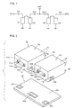
- Fig. 2 is a perspective view showing a specific example of the antenna duplexer shown in Fig. 1.
- the antenna duplexer includes two dielectric filters la and lb, and a coupling board 20.
- Each of the dielectric filters 1a and 1b consists of two stages of resonators.
- dielectric filter la includes an approximately rectangular dielectric block 10a which includes two resonator holes 21a and 22a extending from an apertured surface 11a to the other surface 12a opposing to the apertured surface 11a, and inner conductors 31a and 32a formed on inner peripheral surfaces of resonator holes 21a and 22a, respectively.
- a pair of input/output electrodes 5la and 52a are formed.
- an outer conductor 4a is provided on the outer peripheral surface except the regions on which input/output electrodes 51a and 52a are formed.
- the inner conductors 31a and 32a are not provided at end portions of resonator holes 21a and 22a on the side of the apertured surface (hereinafter referred to as open end surface) 11a, and therefore on this side 11a, inner conductors 31a and 32a are isolated from external conductor 4a (not connected).
- the resonator holes 21a and 22a are connected with the external conductor 4a (short-circuited).
- the other dielectric filter 1b is formed similarly as the above described dielectric filter 1a. Namely, it includes a dielectric block 10b, resonator holes 21b and 22b, inner conductors 31b and 32b, an outer conductor 4b, input and output electrodes 51b and 52b, an open end surface 11b and a short-circuited end surface 12b.
- the coupling board 20 is for coupling two dielectric filters 1a and 1b placed parallel to each other, and it includes input/output electrodes 201 and 202 and an antenna electrode 203 formed on the surface thereof.
- Input/output electrode 201 corresponds to the input/output electrode 51a of one dielectric filter 1a
- input/output electrode 202 corresponds to the input/output electrode 52b of the other dielectric filter 1b
- antenna electrode 203 corresponds to input/output electrodes 52a and 51b of the dielectric filters 1a and 1b.
- a ground conductor 204 is formed on the entire surface of coupling board 20 except the regions where input/output electrodes 201 and 202 and antenna electrode 203 are formed.
- the dielectric filters 1a and 1b structured as described above constitute filters each having two stages of resonators, by the coupling of the resonators formed in resonator holes 21a and 22a, and 21b and 22b, respectively.
- resonators R1 and R2 shown in Fig. 1 represent resonators formed by resonator holes 21a and 22a of dielectric filter 1a
- resonators R3 and R4 represent resonators formed by resonator holes 21b and 22b of dielectric filter 1b.
- the external coupling capacitance Cel between resonator R1 and transmitting terminal TX, the external coupling capacitance Ce4 between resonator R4 and receiving terminal RX and external coupling capacitances Ce2 and Ce3 between resonators R2 and R3 and antenna terminal ANT respectively, are provided by interelectrode capacitances formed between input/output electrodes 51a, 52a, 51b, 52b and corresponding inner conductors 31a, 32a, 31b, and 32b of the dielectric filters 1a, and 1b.
- Another known example of the conventional antenna duplexer includes a number of dielectric resonators each having one resonator hole formed in one dielectric block, arranged parallel to each other.
- external component such as capacitor element is necessary in addition to the coupling board, which results in larger number of parts.
- US-A-5250916 describes a filter duplexer for a radio transceiver.
- a first filter portion of the duplexer filter includes resonators of a first geometric configuration
- a second filter circuit portion of the duplexer filter comprises resonators of a second geometric configuration.
- EP-A-0508734 describes a filter which can be manufactured in a single ceramic block.
- the filter has on one side surface strip-like areas of electrically conducting material located in the area between the resonators of the filter. The dimensions of the strip-like areas are selected so that they substantially cancel the electric and magnetic field between the resonators.
- an antenna duplexer comprising: a dielectric block having a pair of opposing end surfaces; a plurality of resonator holes formed extending from one to the other of the pair of end surfaces of said dielectric block; inner conductors formed on inner peripheral surfaces of said resonator holes; an outer conductor formed on an outer peripheral surface of said dielectric block; and a common electrode and a pair of input/output electrodes electrically coupled to said inner conductors, formed at portions of said outer conductor; wherein said plurality of resonator holes and said plurality of inner conductors provides a portion serving as a transmitting filter and a portion serving as a receiving filter formed in said dielectric block; characterised in that the antenna duplexer further comprises a through hole having an inner conductor which is connected to said outer conductor and is formed between the transmitting filter portion and the receiving filter portion, parallel to said plurality of resonator holes, said through hole being arranged to improve isolation between said transmitting filter portion and said receiving
- two dielectric filters that is, a transmitting filter and a receiving filter, are formed in one dieletric block, input/output electrodes and a common electrode for connection with external circuit are formed on an outer surface of the dielectric block, and the two filters are coupled by the common electrode, so that an antenna duplexer can be formed only by one dielectric block.
- a through hole having an inner conductor conducted to outer conductor is formed parallel to the plurality of resonator holes.
- an inductance can be formed between the common terminal and the ground for absorbing reflected phase of the transmitting filter and the receiving filter.
- an antenna duplexer for use in mobile communications, said antenna duplexer comprising: a single dielectric body, a plurality of resonator holes formed within said dielectric body; and a plurality of electrodes provided as terminals for said duplexer; wherein said plurality of resonator holes and said plurality of electrodes are arranged into portions providing at least one transmitting filter and at least one receiving filter, characterised in that a through hole having an inner conductor is provided between said at least one transmitting and said at least one receiving filter, said through hole being arranged to improve isolation between said at least one transmitting filter and said at least one receiving filter.
- Fig. 1 is an equivalent circuit diagram of a conventional antenna duplexer.
- Fig. 2 is a perspective view of a conventional antenna duplexer.
- Fig. 3 is a perspective view of another conventional duplexer.
- Fig. 4 is a perspective view of an embodiment of the present invention.
- Fig. 5 is a perspective view of another embodiment of the present invention.
- Fig. 6 is an equivalent circuit diagram of the embodiment shown in Fig. 5.
- Fig. 3 is a perspective view of an antenna duplexer.
- the antenna duplexer includes an approximately rectangular parallelepiped dielectric block 1.
- Four resonator holes 2a, 2b, 2c and 2d are formed extending from one to the other of a pair of opposing end surfaces of the dielectric block 1.
- Inner conductors 3a, 3b, 3c and 3d are formed on inner peripheral surfaces of resonators 2a to 2d, respectively.
- an outer conductor 4 is formed except at regions where a pair of input/output electrodes 5a and 5b and one antenna electrode 6 are formed.
- a pair of input/output electrodes 5a and 5b is formed extending from the surface of dielectric block 1 which will be surface-mounted onto the substrate (upper surface of Fig. 3) to one and the other side surfaces of dielectric block 1, respectively, near the open end surface 13a.
- Antenna electrode 6 is formed at the side surface of dielectric block 1 near the open end surface 13a, between the input/output electrodes 5a and 5b.
- Each one end of inner conductors 3a to 3d are isolated from (not connected with) outer conductor 4 which slightly comes into the resonator holes 2a to 2d, since there are portions not provided with any conductor near the open end surface 13a (in other words, the surface of the dielectric block material is exposed in a ring-shape near the end surface 13a around the resonator holes 2a to 2d), while the other ends of the inner conductors 3a to 3d are connected (short-circuited) with outer conductor 4 at the short-circuited end surface 13b opposite to the open end surface 13a.
- Input/output electrodes 5a, 5b and antenna electrode 6 are isolated from outer conductor 4, as there is a non-conductive portion around each of these electrodes.
- the transmitting filter and the receiving filter are coupled sharing the antenna electrode 6, and thus an integrated antenna duplexer having three terminals for input/output, that is, antenna electrode 6 and a pair of input/output electrodes 5a and 5b is provided, which corresponds to the equivalent circuit shown in Fig. 1 of the prior art.
- resonators R1 and R2 shown in Fig. 1 correspond to the resonators formed by resonator holes 2a and 2b, while resonators R3 and R4 correspond to the resonators formed by resonator holes 2c and 2d.
- the external coupling capacitances Ce1 and Ce4 between resonator R1 and transmitting terminal TX and resonator R4 and receiving terminal RX are obtained by interelectrode capacitances formed between input/output electrodes 5a and 5b and inner conductors 3a and 3d of resonator holes 2a and 2d corresponding thereto, while external coupling capacitances Ce2 and Ce3 between resonators R2 and R3 and antenna terminal ANT are obtained by interelectrode capacitances formed between the antenna electrode 6 and inner conductors 3b and 3c of resonator holes 2b and 2c, respectively.
- the surface on which input/output electrodes 5a and 5b and antenna electrode 6 are formed (upper surface of Fig. 3) serves as the bottom surface which is mounted on the substrate.
- an antenna duplexer can be implemented by only one dielectric block 1. Therefore, the number of components can be reduced, the number of manufacturing steps can be decreased and the cost can be reduced.
- Fig. 4 is a perspective view showing an embodiment of the present invention.
- the embodiment shown in Fig. 4 includes a through hole 7 formed between the transmitting and receiving filters of the antenna duplexer of the embodiment shown in Fig. 3, that is, between resonator holes 2b and 2c, parallel to the holes 2b and 2c.
- An inner conductor 3e is formed on the inner peripheral surface of through hole 7, and the conductor is connected (short-circuited) with the outer conductor 4 at both end surfaces, that is, the open end surface 13a and the short-circuited end surface 13b.
- Other structures are the same as those of Fig. 3.
- Fig. 5 is a perspective view showing still another embodiment of the present invention
- Fig. 6 is an equivalent circuit diagram of the embodiment shown in Fig. 5.
- a through hole 8 is formed between the transmitting filter and the receiving filter of the antenna duplexer shown in Fig. 3, that is, between resonators 2b and 2c, parallel to the resonators 2b and 2c.
- An inner conductor 3f is formed on the inner peripheral surface of the through hole 8, and a through hole 9 is further provided which connects (conducts) inner conductor 3f to antenna electrode 6.
- one end of inner conductor 3f formed on the inner peripheral surface of through hole 8 is isolated from outer conductor 4 as there is a portion not provided with any conductor near the open end surface 13a, while it is conducted with outer conductor 4 at the short-circuited end surface 13b.
- Other structures are the same as those of Fig. 3.
- an inductance L such as shown in Fig. 6 is formed between antenna electrode 6 and outer conductor 4, by the inner conductor 3f of the through hole 8 connected to antenna electrode 6 by means of through hole 9.
- the inductance L is capable of absorbing or annulling reflected phase or susceptance of the transmitting filter and the receiving filter between the antenna terminal ANT and the ground.
- the transmitting filter and the receiving filter are provided by one dielectric block 1, and input/output electrodes 5a and 5b and antenna electrode 6 for connection to an outer circuit are formed on an outer surface of dielectric block 1, and therefore a component such as coupling board used in the conventional antenna duplexer becomes unnecessary.
- an antenna duplexer having an inductance for absorbing reflected phase of transmitting and receiving filters inserted between antenna terminal ANT and the ground can be provided by one dielectric block.
- the shape, location and the like of the input/output electrodes 5a, 5b and antenna electrode 6 of respective embodiments are not limited to those disclosed, and the shape, dimension, positions may be arbitrarily changed so as to change the capacitance values, and to provide aimed filter characteristics.
- Isolation between the outer conductor and the inner conductor on the side of the open end surface 13a is implemented by not providing the inner conductor near the open end surface 13a in the embodiments described above. However, it is not limited to this, and a non-conducting portion may be provided on the open end surface 13a. Namely, one end in the axial direction of the inner conductor may reach the open end surface 13a. Alternatively, the outer conductor may not be provided at all on the open end surfaces 13a.
- a resonator hole has a constant diameter in the embodiments above, the diameter of the resonator hole may be changed midway, and a coupling groove for changing the degree of coupling between each of the resonators may be provided at the top and bottom surfaces of dielectric block 1, or a coupling hole for changing the degree of coupling between each of the resonators may be provided between the resonators.
- each filter may be constituted by three or more stages of resonators including three or more resonator holes.
Landscapes
- Control Of Motors That Do Not Use Commutators (AREA)
Claims (5)
- Ein Antennenduplexer mit folgenden Merkmalen:einem dielektrischen Block (1) mit einem Paar von gegenüberliegenden Endoberflächen (13a, 13b);einer Mehrzahl von Resonatorlöchern (2a bis 2d), die sich von einer zu der anderen des Paar von Endoberflächen (13a, 13b) des dielektrischen Blocks (1) erstreckend gebildet sind;inneren Leitern (3a bis 3d), die auf inneren peripheren Oberflächen der Resonatorlöcher (2a bis 2d) gebildet sind;einem äußeren Leiter (4), der auf einer äußeren peripheren Oberfläche des dielektrischen Blocks gebildet ist (1); undeiner gemeinsamen Elektrode (6) und einem Paar von Eingangs/Ausgangs-Elektroden (5a, 5b), die mit den inneren Leitern (3a bis 3d) elektrisch gekoppelt sind und an Abschnitten des äußeren Leiters (4) gebildet sind; wobeidie Mehrzahl von Resonatorlöchern (2a bis 2d) und die Mehrzahl von inneren Leitern (3a bis 3d) einen Abschnitt (R1, R2) liefern, der als ein Sendefilter dient, und einen Abschnitt (R3, R4) liefern, der als ein Empfangsfilter dient, die in dem dielektrischen Block (1) gebildet sind; dadurch gekennzeichnet, daß der Antennenduplexer ferner ein Durchgangsloch (7) mit einem inneren Leiter (3e), der mit dem äußeren Leiter (4) verbunden ist, das zwischen dem Sendefilterabschnitt (R1, R2) und dem Empfangsfilterabschnitt (R3, R4) parallel zu der Mehrzahl von Resonatorlöchern (2a bis 2d) gebildet ist, aufweist, wobei das Durchgangsloch (7) angeordnet ist, um eine Trennung zwischen dem Sendefilterabschnitt (R1, R2) und dem Empfangsfilterabschnitt (R3, R4) zu verbessern.
- Der Antennenduplexer gemäß Anspruch 1, der ferner folgende Merkmale aufweist:ein Verbindungsbauglied (9) zum elektrischen Verbinden eines Endes des inneren Leiters (3f) des Durchgangslochs (8) mit der gemeinsamen Elektrode (6); wobeider innere Leiter (3f) des Durchgangslochs (8) mit dem äußeren Leiter (4) an dem anderen Ende verbunden ist (Fig. 5).
- Der Antennenduplexer gemäß Anspruch 2, bei dem das Verbindungsbauglied (9) und das Durchgangsloch (8) angeordnet sind, um einen Induktor (L) zu bilden (Fig. 5).
- Der Antennenduplexer gemäß einem beliebigen vorhergehenden Anspruch, bei demdas Paar von Eingangs/Ausgangs-Elektroden (5a, 5b) Elektroden aufweist, die an Ecken vorgesehen sind, die aus Seitenoberflächen und einer Ebene zwischen der einen und der anderen des Paars von Endoberflächen (13a, 13b) gebildet sind, unddie gemeinsame Elektrode (6) eine Elektrode aufweist, die auf der Ebene zwischen dem Paar von Eingangs/Ausgangs-Elektroden (5a, 5b) gebildet ist.
- Ein Antennenduplexer zur Verwendung bei der mobil Kommunikation, wobei der Antennenduplexer folgende Merkmale aufweist:einen einzigen dielektrischen Körper (1),eine Mehrzahl von Resonatorlöchern (2a bis 2d), die innerhalb des dielektrischen Körpers (1) gebildet sind;eine Mehrzahl von Elektroden (5a, 5b, 6), die als Anschlüsse für den Duplexer vorgesehen sind;wobei die Mehrzahl von Resonatorlöchern (2a bis 2d) und die Mehrzahl von Elektroden (5a, 5b, 6) in Abschnitte angeordnet sind, die mindestens ein Sendefilter (R1, R2) und mindestens ein Empfangsfilter (R3, R4) liefern, dadurch gekennzeichnet, daß ein Durchgangsloch (7) mit einem inneren Leiter (3e) zwischen dem mindestens einen Sendefilter (R1, R2) und dem mindestens einen Empfangsfilter (R3, R4) vorgesehen ist, wobei das Durchgangsloch (7) angeordnet ist, um die Trennung zwischen dem mindestens einen Sendefilter (R1, R2) und dem mindestens einen Empfangsfilter (R3, R4) zu verbessern.
Applications Claiming Priority (2)
| Application Number | Priority Date | Filing Date | Title |
|---|---|---|---|
| JP289400/93 | 1993-11-18 | ||
| JP28940093A JP3230353B2 (ja) | 1993-11-18 | 1993-11-18 | アンテナ共用器 |
Publications (2)
| Publication Number | Publication Date |
|---|---|
| EP0654841A1 EP0654841A1 (de) | 1995-05-24 |
| EP0654841B1 true EP0654841B1 (de) | 1999-05-19 |
Family
ID=17742743
Family Applications (1)
| Application Number | Title | Priority Date | Filing Date |
|---|---|---|---|
| EP94308520A Expired - Lifetime EP0654841B1 (de) | 1993-11-18 | 1994-11-18 | Antennenweiche |
Country Status (6)
| Country | Link |
|---|---|
| US (1) | US5686873A (de) |
| EP (1) | EP0654841B1 (de) |
| JP (1) | JP3230353B2 (de) |
| KR (1) | KR0167806B1 (de) |
| DE (1) | DE69418573T2 (de) |
| TW (1) | TW301811B (de) |
Families Citing this family (21)
| Publication number | Priority date | Publication date | Assignee | Title |
|---|---|---|---|---|
| US6008707A (en) * | 1993-11-18 | 1999-12-28 | Murata Manufacturing Co., Ltd. | Antenna duplexer |
| JP3119176B2 (ja) * | 1996-10-23 | 2000-12-18 | 株式会社村田製作所 | 誘電体線路用アンテナ共用分配器および送受信装置 |
| KR100198944B1 (ko) * | 1996-11-05 | 1999-06-15 | 이계철 | 이중 결합 선로 특성을 갖는 듀플렉서 |
| US6052040A (en) * | 1997-03-03 | 2000-04-18 | Ngk Spark Plug Co., Ltd. | Dielectric duplexer with different capacitive coupling between antenna pad and transmitting and receiving sections |
| JPH10335906A (ja) * | 1997-03-31 | 1998-12-18 | Murata Mfg Co Ltd | 誘電体フィルタ、誘電体デュプレクサ及び通信機装置 |
| JPH10308607A (ja) * | 1997-05-07 | 1998-11-17 | Ngk Spark Plug Co Ltd | 誘電体デュプレクサ装置 |
| JPH11122139A (ja) * | 1997-10-17 | 1999-04-30 | Murata Mfg Co Ltd | アンテナ共用器 |
| JP3387422B2 (ja) * | 1998-08-25 | 2003-03-17 | 株式会社村田製作所 | アンテナ共用器及び通信機装置 |
| JP3344333B2 (ja) * | 1998-10-22 | 2002-11-11 | 株式会社村田製作所 | フィルタ内蔵誘電体アンテナ、デュプレクサ内蔵誘電体アンテナおよび無線装置 |
| US6181223B1 (en) * | 1998-12-29 | 2001-01-30 | Ngk Spark Plug Co., Ltd. | Dielectric duplexer device |
| DE19903855B4 (de) * | 1999-02-01 | 2010-04-15 | Epcos Ag | Antennenweiche |
| JP2002026602A (ja) | 2000-07-10 | 2002-01-25 | Murata Mfg Co Ltd | 誘電体共振器装置、フィルタ、デュプレクサおよび通信装置 |
| JP3317404B1 (ja) * | 2001-07-25 | 2002-08-26 | ティーディーケイ株式会社 | 誘電体装置 |
| JP3329450B1 (ja) * | 2001-09-28 | 2002-09-30 | ティーディーケイ株式会社 | 誘電体装置 |
| DE10322136B4 (de) * | 2003-05-16 | 2011-05-19 | Epcos Ag | Frontend-Modul mit geringer Einfügedämpfung |
| EP1644475A4 (de) * | 2003-06-20 | 2009-06-03 | Isis Pharmaceuticals Inc | Doppelstrang-zusammensetzungen mit einem 3'-endo-modifizierten strang zur verwendung bei der genmodulation |
| DE102004001347B3 (de) * | 2004-01-08 | 2005-07-07 | Epcos Ag | Duplexer mit niedriger Bauhöhe |
| US9030275B2 (en) | 2008-12-09 | 2015-05-12 | Cts Corporation | RF monoblock filter with recessed top pattern and cavity providing improved attenuation |
| US9030276B2 (en) | 2008-12-09 | 2015-05-12 | Cts Corporation | RF monoblock filter with a dielectric core and with a second filter disposed in a side surface of the dielectric core |
| JP2012514954A (ja) * | 2009-01-08 | 2012-06-28 | シーティーエス・コーポレーション | 凹型上部パターンとキャビティを具備した複式フィルタ |
| US9030272B2 (en) | 2010-01-07 | 2015-05-12 | Cts Corporation | Duplex filter with recessed top pattern and cavity |
Family Cites Families (18)
| Publication number | Priority date | Publication date | Assignee | Title |
|---|---|---|---|---|
| JPS5773501A (en) * | 1980-10-25 | 1982-05-08 | Fujitsu Ltd | Dielectric filter element and dielectric filter |
| US4742562A (en) * | 1984-09-27 | 1988-05-03 | Motorola, Inc. | Single-block dual-passband ceramic filter useable with a transceiver |
| JPS61161806A (ja) * | 1985-01-11 | 1986-07-22 | Mitsubishi Electric Corp | 高周波ろ波器 |
| JPS62169503A (ja) * | 1986-01-21 | 1987-07-25 | Tdk Corp | 一体型共用器 |
| JPS62217701A (ja) * | 1986-03-19 | 1987-09-25 | Fujitsu Ltd | 分波器 |
| US5103197A (en) * | 1989-06-09 | 1992-04-07 | Lk-Products Oy | Ceramic band-pass filter |
| FI87853C (fi) * | 1991-04-12 | 1993-02-25 | Lk Products Oy | Keramiskt spaerrfilter |
| US5241693A (en) * | 1989-10-27 | 1993-08-31 | Motorola, Inc. | Single-block filter for antenna duplexing and antenna-switched diversity |
| JPH0484501A (ja) * | 1990-07-27 | 1992-03-17 | Oki Electric Ind Co Ltd | 分波器 |
| JPH04103203A (ja) * | 1990-08-22 | 1992-04-06 | Murata Mfg Co Ltd | 誘電体フィルタ |
| US5216394A (en) * | 1991-07-19 | 1993-06-01 | Uniden Corporation | Dielectric multi-line resonator including a coupling conductor line mainly inductively coupled to a resonator conductor line |
| JP2910807B2 (ja) * | 1991-10-25 | 1999-06-23 | 株式会社村田製作所 | 誘電体共振器装置、誘電体フィルタおよびそれらの製造方法 |
| US5250916A (en) | 1992-04-30 | 1993-10-05 | Motorola, Inc. | Multi-passband dielectric filter construction having filter portions with dissimilarly-sized resonators |
| JPH06132706A (ja) * | 1992-09-07 | 1994-05-13 | Murata Mfg Co Ltd | 誘電体共振部品 |
| US5379011A (en) * | 1992-10-23 | 1995-01-03 | Motorola, Inc. | Surface mount ceramic filter duplexer having reduced input/output coupling and adjustable high-side transmission zeroes |
| TW225047B (en) * | 1992-12-16 | 1994-06-11 | Daiichi Denpa Kogyo Kk | A linkup device and a antenna device of a co-axial cable |
| US5537082A (en) * | 1993-02-25 | 1996-07-16 | Murata Manufacturing Co., Ltd. | Dielectric resonator apparatus including means for adjusting the degree of coupling |
| JP3309483B2 (ja) * | 1993-04-12 | 2002-07-29 | 松下電器産業株式会社 | 誘電体フィルタ |
-
1993
- 1993-11-18 JP JP28940093A patent/JP3230353B2/ja not_active Expired - Lifetime
-
1994
- 1994-11-16 US US08/340,542 patent/US5686873A/en not_active Expired - Lifetime
- 1994-11-17 KR KR1019940030151A patent/KR0167806B1/ko not_active Expired - Lifetime
- 1994-11-17 TW TW083110655A patent/TW301811B/zh not_active IP Right Cessation
- 1994-11-18 DE DE69418573T patent/DE69418573T2/de not_active Expired - Lifetime
- 1994-11-18 EP EP94308520A patent/EP0654841B1/de not_active Expired - Lifetime
Also Published As
| Publication number | Publication date |
|---|---|
| US5686873A (en) | 1997-11-11 |
| DE69418573T2 (de) | 1999-09-16 |
| JPH07142910A (ja) | 1995-06-02 |
| KR950015850A (ko) | 1995-06-17 |
| EP0654841A1 (de) | 1995-05-24 |
| JP3230353B2 (ja) | 2001-11-19 |
| KR0167806B1 (ko) | 1999-02-01 |
| DE69418573D1 (de) | 1999-06-24 |
| TW301811B (de) | 1997-04-01 |
Similar Documents
| Publication | Publication Date | Title |
|---|---|---|
| EP0654841B1 (de) | Antennenweiche | |
| US6696903B1 (en) | Laminated dielectric filter, and antenna duplexer and communication equipment using the same | |
| EP0617478B1 (de) | Geschichteter dielektrischer Resonator und dielektrisches Filter | |
| KR0147726B1 (ko) | 유전체 필터 | |
| US20070176712A1 (en) | High frequency filter | |
| US7443262B2 (en) | Two-port isolator, characteristic adjusting method therefor, and communication apparatus | |
| US6008707A (en) | Antenna duplexer | |
| KR100401963B1 (ko) | 유전체 공진기, 유전체 필터, 유전체 듀플렉서 및 이들을사용한 통신장치 | |
| US5977848A (en) | Polar dielectric filter and dielectric duplexer incorporating same | |
| JP3329450B1 (ja) | 誘電体装置 | |
| KR100394805B1 (ko) | 유전체 필터, 안테나 공용기 및 통신기 장치 | |
| US7005949B2 (en) | Dielectric filter | |
| US7535318B2 (en) | Dielectric device | |
| US6747527B2 (en) | Dielectric duplexer and communication apparatus | |
| US6369668B1 (en) | Duplexer and communication apparatus including the same | |
| US6798311B2 (en) | Nonreciprocal circuit device with a solenoid-shaped inductor generating perpendicular flux | |
| US20260025118A1 (en) | Filter device and radio-frequency front-end circuit | |
| KR200167764Y1 (ko) | 듀플렉서 | |
| JPH11261398A (ja) | 複合スイッチ回路及び複合スイッチ回路部品 | |
| KR19990049687A (ko) | 듀플렉스 유전체 필터 | |
| KR100258788B1 (ko) | 동축선 공진기의 절반구조를 이용한 대역 통과 여파기 | |
| US6642817B2 (en) | Dielectric filter, dielectric duplexer, and communication device | |
| JPH0846403A (ja) | 誘電体フィルタ用基板及び誘電体フィルタ | |
| JPH0597106U (ja) | 誘電体フィルタ |
Legal Events
| Date | Code | Title | Description |
|---|---|---|---|
| PUAI | Public reference made under article 153(3) epc to a published international application that has entered the european phase |
Free format text: ORIGINAL CODE: 0009012 |
|
| AK | Designated contracting states |
Kind code of ref document: A1 Designated state(s): DE FR GB |
|
| 17P | Request for examination filed |
Effective date: 19950501 |
|
| 17Q | First examination report despatched |
Effective date: 19970904 |
|
| GRAG | Despatch of communication of intention to grant |
Free format text: ORIGINAL CODE: EPIDOS AGRA |
|
| GRAG | Despatch of communication of intention to grant |
Free format text: ORIGINAL CODE: EPIDOS AGRA |
|
| GRAG | Despatch of communication of intention to grant |
Free format text: ORIGINAL CODE: EPIDOS AGRA |
|
| GRAH | Despatch of communication of intention to grant a patent |
Free format text: ORIGINAL CODE: EPIDOS IGRA |
|
| GRAH | Despatch of communication of intention to grant a patent |
Free format text: ORIGINAL CODE: EPIDOS IGRA |
|
| GRAA | (expected) grant |
Free format text: ORIGINAL CODE: 0009210 |
|
| AK | Designated contracting states |
Kind code of ref document: B1 Designated state(s): DE FR GB |
|
| REF | Corresponds to: |
Ref document number: 69418573 Country of ref document: DE Date of ref document: 19990624 |
|
| ET | Fr: translation filed | ||
| PLBE | No opposition filed within time limit |
Free format text: ORIGINAL CODE: 0009261 |
|
| STAA | Information on the status of an ep patent application or granted ep patent |
Free format text: STATUS: NO OPPOSITION FILED WITHIN TIME LIMIT |
|
| 26N | No opposition filed | ||
| REG | Reference to a national code |
Ref country code: GB Ref legal event code: IF02 |
|
| PGFP | Annual fee paid to national office [announced via postgrant information from national office to epo] |
Ref country code: FR Payment date: 20131108 Year of fee payment: 20 Ref country code: GB Payment date: 20131113 Year of fee payment: 20 Ref country code: DE Payment date: 20131113 Year of fee payment: 20 |
|
| REG | Reference to a national code |
Ref country code: DE Ref legal event code: R071 Ref document number: 69418573 Country of ref document: DE |
|
| REG | Reference to a national code |
Ref country code: GB Ref legal event code: PE20 Expiry date: 20141117 |
|
| PG25 | Lapsed in a contracting state [announced via postgrant information from national office to epo] |
Ref country code: GB Free format text: LAPSE BECAUSE OF EXPIRATION OF PROTECTION Effective date: 20141117 |