EP0655785B1 - Nichtflüchtige Halbleiterspeicheranordnung und Verfahren zur Herstellung - Google Patents
Nichtflüchtige Halbleiterspeicheranordnung und Verfahren zur Herstellung Download PDFInfo
- Publication number
- EP0655785B1 EP0655785B1 EP94118861A EP94118861A EP0655785B1 EP 0655785 B1 EP0655785 B1 EP 0655785B1 EP 94118861 A EP94118861 A EP 94118861A EP 94118861 A EP94118861 A EP 94118861A EP 0655785 B1 EP0655785 B1 EP 0655785B1
- Authority
- EP
- European Patent Office
- Prior art keywords
- region
- mos transistor
- gate electrode
- data storage
- insulating film
- Prior art date
- Legal status (The legal status is an assumption and is not a legal conclusion. Google has not performed a legal analysis and makes no representation as to the accuracy of the status listed.)
- Expired - Lifetime
Links
- 239000004065 semiconductor Substances 0.000 title claims description 68
- 238000004519 manufacturing process Methods 0.000 title claims description 12
- 238000013500 data storage Methods 0.000 claims description 105
- 239000000758 substrate Substances 0.000 claims description 92
- 239000012535 impurity Substances 0.000 claims description 84
- 238000009792 diffusion process Methods 0.000 claims description 25
- 238000000034 method Methods 0.000 claims description 15
- 230000006870 function Effects 0.000 claims description 6
- OAICVXFJPJFONN-UHFFFAOYSA-N Phosphorus Chemical compound [P] OAICVXFJPJFONN-UHFFFAOYSA-N 0.000 claims description 4
- 229910052698 phosphorus Inorganic materials 0.000 claims description 4
- 239000011574 phosphorus Substances 0.000 claims description 4
- 230000005689 Fowler Nordheim tunneling Effects 0.000 claims description 3
- 229910052785 arsenic Inorganic materials 0.000 claims description 2
- RQNWIZPPADIBDY-UHFFFAOYSA-N arsenic atom Chemical compound [As] RQNWIZPPADIBDY-UHFFFAOYSA-N 0.000 claims description 2
- 238000005530 etching Methods 0.000 claims description 2
- VYPSYNLAJGMNEJ-UHFFFAOYSA-N Silicium dioxide Chemical compound O=[Si]=O VYPSYNLAJGMNEJ-UHFFFAOYSA-N 0.000 description 48
- 229910052814 silicon oxide Inorganic materials 0.000 description 48
- 239000010410 layer Substances 0.000 description 28
- 229910021420 polycrystalline silicon Inorganic materials 0.000 description 13
- 229920005591 polysilicon Polymers 0.000 description 13
- 230000005641 tunneling Effects 0.000 description 13
- 230000007423 decrease Effects 0.000 description 6
- 230000000694 effects Effects 0.000 description 6
- 230000008878 coupling Effects 0.000 description 5
- 238000010168 coupling process Methods 0.000 description 5
- 238000005859 coupling reaction Methods 0.000 description 5
- 230000008569 process Effects 0.000 description 5
- XUIMIQQOPSSXEZ-UHFFFAOYSA-N Silicon Chemical compound [Si] XUIMIQQOPSSXEZ-UHFFFAOYSA-N 0.000 description 2
- 230000015572 biosynthetic process Effects 0.000 description 2
- 230000008859 change Effects 0.000 description 2
- 230000010354 integration Effects 0.000 description 2
- 230000009467 reduction Effects 0.000 description 2
- 229910052710 silicon Inorganic materials 0.000 description 2
- 239000010703 silicon Substances 0.000 description 2
- 229910052581 Si3N4 Inorganic materials 0.000 description 1
- 230000008901 benefit Effects 0.000 description 1
- 239000000969 carrier Substances 0.000 description 1
- 230000015556 catabolic process Effects 0.000 description 1
- 230000000593 degrading effect Effects 0.000 description 1
- 230000005684 electric field Effects 0.000 description 1
- 239000007943 implant Substances 0.000 description 1
- 238000002347 injection Methods 0.000 description 1
- 239000007924 injection Substances 0.000 description 1
- 239000005001 laminate film Substances 0.000 description 1
- 230000003647 oxidation Effects 0.000 description 1
- 238000007254 oxidation reaction Methods 0.000 description 1
- 238000005036 potential barrier Methods 0.000 description 1
- 230000000630 rising effect Effects 0.000 description 1
- HQVNEWCFYHHQES-UHFFFAOYSA-N silicon nitride Chemical compound N12[Si]34N5[Si]62N3[Si]51N64 HQVNEWCFYHHQES-UHFFFAOYSA-N 0.000 description 1
- 239000002356 single layer Substances 0.000 description 1
Images



Classifications
-
- H—ELECTRICITY
- H10—SEMICONDUCTOR DEVICES; ELECTRIC SOLID-STATE DEVICES NOT OTHERWISE PROVIDED FOR
- H10B—ELECTRONIC MEMORY DEVICES
- H10B41/00—Electrically erasable-and-programmable ROM [EEPROM] devices comprising floating gates
- H10B41/30—Electrically erasable-and-programmable ROM [EEPROM] devices comprising floating gates characterised by the memory core region
-
- H—ELECTRICITY
- H10—SEMICONDUCTOR DEVICES; ELECTRIC SOLID-STATE DEVICES NOT OTHERWISE PROVIDED FOR
- H10B—ELECTRONIC MEMORY DEVICES
- H10B41/00—Electrically erasable-and-programmable ROM [EEPROM] devices comprising floating gates
- H10B41/30—Electrically erasable-and-programmable ROM [EEPROM] devices comprising floating gates characterised by the memory core region
- H10B41/35—Electrically erasable-and-programmable ROM [EEPROM] devices comprising floating gates characterised by the memory core region with a cell select transistor, e.g. NAND
-
- H—ELECTRICITY
- H10—SEMICONDUCTOR DEVICES; ELECTRIC SOLID-STATE DEVICES NOT OTHERWISE PROVIDED FOR
- H10B—ELECTRONIC MEMORY DEVICES
- H10B69/00—Erasable-and-programmable ROM [EPROM] devices not provided for in groups H10B41/00 - H10B63/00, e.g. ultraviolet erasable-and-programmable ROM [UVEPROM] devices
-
- H—ELECTRICITY
- H10—SEMICONDUCTOR DEVICES; ELECTRIC SOLID-STATE DEVICES NOT OTHERWISE PROVIDED FOR
- H10D—INORGANIC ELECTRIC SEMICONDUCTOR DEVICES
- H10D30/00—Field-effect transistors [FET]
- H10D30/60—Insulated-gate field-effect transistors [IGFET]
- H10D30/68—Floating-gate IGFETs
- H10D30/681—Floating-gate IGFETs having only two programming levels
- H10D30/683—Floating-gate IGFETs having only two programming levels programmed by tunnelling of carriers, e.g. Fowler-Nordheim tunnelling
-
- H—ELECTRICITY
- H10—SEMICONDUCTOR DEVICES; ELECTRIC SOLID-STATE DEVICES NOT OTHERWISE PROVIDED FOR
- H10D—INORGANIC ELECTRIC SEMICONDUCTOR DEVICES
- H10D30/00—Field-effect transistors [FET]
- H10D30/60—Insulated-gate field-effect transistors [IGFET]
- H10D30/68—Floating-gate IGFETs
- H10D30/6891—Floating-gate IGFETs characterised by the shapes, relative sizes or dispositions of the floating gate electrode
-
- Y—GENERAL TAGGING OF NEW TECHNOLOGICAL DEVELOPMENTS; GENERAL TAGGING OF CROSS-SECTIONAL TECHNOLOGIES SPANNING OVER SEVERAL SECTIONS OF THE IPC; TECHNICAL SUBJECTS COVERED BY FORMER USPC CROSS-REFERENCE ART COLLECTIONS [XRACs] AND DIGESTS
- Y10—TECHNICAL SUBJECTS COVERED BY FORMER USPC
- Y10S—TECHNICAL SUBJECTS COVERED BY FORMER USPC CROSS-REFERENCE ART COLLECTIONS [XRACs] AND DIGESTS
- Y10S438/00—Semiconductor device manufacturing: process
- Y10S438/981—Utilizing varying dielectric thickness
Definitions
- This invention relates to a nonvolatile semiconductor memory device capable of electrically rewriting data and semipermanently retaining data.
- Nonvolatile semiconductor memory devices using double-gate MOS transistors with a floating gate and a control gate are well known.
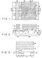
- a conventional nonvolatile semiconductor memory device will be explained with reference to FIGS. 1 to 10.
- FIGS. 1 and 2 show a first structure of a conventional nonvolatile semiconductor memory device.
- FIG. 1 is a plan view of a memory cell in the nonvolatile semiconductor memory device.
- FIG. 2 is a sectional view taken along line II-II' of FIG. 1.
- the memory cell is composed of a data storage MOS transistor MT and a select MOS transistor ST, which are connected to each other in series.
- the source region of the select MOS transistor ST and the drain region of the data storage MOS transistor MT are made up of n-type regions 12 and 13 at the surface of a p-type semiconductor substrate 10, respectively.
- a floating-gate electrode 19 and a control gate electrode 20 are formed on and above the channel region 22 of the data storage MOS transistor MT and the silicon oxide film 17.
- the floating-gate electrode 19 and control gate electrode 20 are made of polysilicon, for example.
- silicon oxide films 23, 16 (of several tens nm) several times as thick as the silicon oxide film 17 are formed.
- the drain region of the select MOS transistor ST is composed of n-type regions 11, 12', and the source region of the data storage MOS transistor MT is made up of n-type regions 14, 15.
- the erasing of data is effected by applying a high potential to the control gate electrode 20 of the data storage MOS transistor MT. Specifically, once a high potential has been applied to the control gate electrode 20, Fowler-Nordheim tunneling allows electrons to move from the n-type region (drain region) 13 via the silicon oxide film 17 to the floating-gate electrode 19.
- the writing of data is performed by applying a high potential to the n-type region (drain region) 11 and the gate electrode 18 of the select MOS transistor ST, and 0V to the control gate electrode 20 of the data storage MOS transistor MT.
- the n-type regions (drain region) 12, 13 of the data storage MOS transistor MT are at a high potential, so that the tunnel effect allows electrons to move from the floating-gate electrode 19 to the drain region via the silicon oxide film 17.
- the n-type region (drain region) 13 of the data storage MOS transistor is formed directly under the floating-gate electrode 19 before the floating-gate electrode 19 is formed.
- the n-type region (source region) 15 of the data storage MOS transistor MT is formed in a self-aligning manner by implanting n-type impurities into the substrate 10 using the floating-gate electrode 29 and control gate electrode 20 as a mask.
- the channel length of the data storage MOS transistor MT is the distance between the n-type region 13 and the n-type region 15. Therefore, the channel length of the data storage MOS transistor MT varies depending on the misalignment of the mask for forming the n-type region 13 from the mask for forming a polysilicon mask used in forming the n-type region 15.
- n-type impurities are implanted into region D enclosed by a dot-dash line in FIG. 1, thereby forming the n-type region 13 and n-type region 14 at the same time.
- the channel length of the data storage MOS transistor MT is the distance between the n-type region 13 and the n-type region 14. Since the n-type regions 13, 14 are formed with the same mask, the channel length of the data storage MOS transistor MT is always constant. As a result, the channel length of the data storage MOS transistor MT will not vary due to mask misalignment.
- this method has a disadvantage in that, to assure the formation of the n-type region 14 directly under the floating-gate electrode 19, the floating-gate electrode 19 must be lengthened along the channel length of the data storage MOS transistor MT, by the sum of the amount of misalignment of the mask for forming the floating-gate electrode 19 and the amount of misalignment of the mask for forming the n-type regions 13, 14.
- the thin silicon oxide film 17 of nearly 10 nm in thickness between the n-type region 13 and the floating-gate electrode 19 will be examined.
- the silicon oxide film 17 is formed by removing the thick silicon oxide films 16, 23 of several tens nm in thickness using a mask with an opening in area F in FIG. 1 and then performing thermal oxidation.
- the thin silicon oxide film 17 must be formed on the n-type region 13 and directly under the floating-gate electrode 19.
- the floating-gate electrode 19 must be lengthened along the channel length by the sum of the amount of misalignment of the mask for forming the floating-gate electrode 19 from the mask for forming an opening in area F and the amount of misalignment of the mask for forming an opening in area F from the mask for forming the n-type region 13.
- the minimum dimension along the channel of the data storage MOS transistor MT in the memory cell is determined as shown in FIG. 3.
- the minimum dimension along the channel of the data storage MOS transistor MT is determined by the sum of the following:
- the memory cell of the structure shown in FIGS. 1 and 2 requires a lot of misalignments to be taken into account in designing, as compared with an ordinary MOS transistor having a self-aligning structure, and therefore has the disadvantage of resulting in larger memory cells.
- the gate oxide film of the select MOS transistor ST is several times as thick as the gate oxide film of a MOS transistor to which only an ordinary power-supply voltage (e.g., 5V) is applied.
- an ordinary power-supply voltage e.g., 5V
- the gate oxide film of the data storage MOS transistor MT and the gate oxide film of the select MOS transistor ST are formed simultaneously.
- the gate oxide film of the data storage MOS transistor MT is as thick as the gate oxide film of the select MOS transistor ST.
- the gate oxide film of the data storage MOS transistor MT is as thick as the gate oxide film of the select MOS transistor ST, that is, several times as thick as the gate oxide film of an ordinary MOS transistor. For this reason, the channel length of the data storage MOS transistor MT is larger than the channel length of an ordinary MOS transistor.
- the potential of the floating gate when a high potential is applied to the drain region is determined by the capacitive coupling between the drain region and the floating gate.
- the capacitive coupling between the drain region and the floating gate of the data storage MOS transistor MT varies according to the misalignment of the mask for forming the n-type region 13 from the mask for forming the floating-gate electrode 19.
- the variation in the capacitive coupling results in a variation in the amount of electrons released from the floating-gate electrode into the drain region.
- this causes variations in the threshold voltage of the data storage MOS transistor MT after electrons have been released.
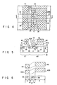
- FIGS. 4 and 5 show a double structure of a conventional nonvolatile semiconductor memory device.
- FIG. 4 is a plan view of a conventional nonvolatile semiconductor memory device.
- FIG. 5 is a sectional view taken along line V-V'.
- the conventional nonvolatile semiconductor memory device has been disclosed in Jpn. Pat. Appln. KOKAI Publication No. 63-84168.
- the memory cell is composed of a data storage MOS transistor MT and a select MOS transistor ST, which are connected to each other in series.
- a first portion 40B of a floating-gate electrode is provided via a gate insulating film 37 of several tens nm in thickness.
- a second portion 40A of the floating-gate electrode is provided on the gate insulating film 36.
- first portion 40B and second portion 40A of the floating-gate electrode are spaced apart, they are electrically connected to each other above a field region.
- an insulating film 42 and a control gate electrode 44 are provided on and above the first portion 40B and second portion 40A of the floating-gate electrode. It is preferable that the shape of the control gate electrode 44 should be the same as that of the floating-gate electrode.
- the source region of the select MOS transistor ST and the drain region of the data storage MOS transistor are made up of n-type regions 32, 33, 34 formed continuously at the surface of a p-type semiconductor substrate 30.
- the drain region of the select MOS transistor ST is made up of n-type regions 31, 32', and an n-type region 35 is the source region of the data storage MOS transistor MT.
- the n-type region 33 is formed before the formation of the floating-gate electrode and control gate electrode, as with the conventional device of FIGS. 1 and 2.
- the n-type region 33 is formed by implanting n-type impurities into area E of the substrate 30 enclosed by a dot-dash line in FIG. 4.
- the n-type regions 32', 32, 34 are formed in a self-aligning manner by implanting n-type impurities into the substrate 30 using the floating-gate electrodes 40A, 40B and control gate electrode 44 as a mask.
- the n-type regions 31, 35 are formed by implanting n-type impurities into the substrate 30 using a specific mask.
- the capacitive coupling between the n-type regions (drain region) 32 to 34 and the floating-gate electrodes 40A, 40B is determined by the area of the portion where the n-type region (drain region) 33 overlaps with the second portion 40A of the floating-gate electrode and the area is constant regardless of mask misalignment.
- the n-type regions 34, 35 can be formed in a self-aligning manner using the floating-gate electrodes 40A, 40B and control gate electrode 44 as a mask. Therefore, it is not necessary to take into account a misalignment of the mask for forming the n-type regions 34, 35 and a misalignment of the masks for forming the floating-gate electrodes 40A, 40B and control gate electrode 44.
- the minimum dimension along the channel length of the data storage MOS transistor MT is shown in FIG. 6.
- the minimum dimension along the channel length of the data storage MOS transistor MT is determined by the sum of the following:
- the minimum spacing (expressed by “e") in which the floating-gate electrode and control gate electrode (polysilicon) can be processed is greater than b+c, the minimum dimension is determined by a+d+e.
- FIGS. 1 and 2 is compared with the conventional device in FIGS. 4 and 5.
- the data storage MOS transistor MT of FIG. 6 can be made smaller by the length of e.
- the dimensions of a memory cell can be made smaller than those of a memory cell in the conventional device of FIGS. 1 and 2.
- the thickness of the gate oxide film 37 of the data storage MOS transistor MT is larger. Accordingly, the channel length of the data storage MOS transistor MT is larger, so that the area of the memory cell cannot be made much smaller than that of the memory cell in the conventional device of FIGS. 1 and 2.
- FIG. 7 shows a third structure of a conventional nonvolatile semiconductor memory device.
- FIG. 8 is a sectional view taken along line VIII-VIII' of FIG. 7.
- the memory cell is composed of a data storage MOS transistor MT and a select MOS transistor ST, which are connected to each other in series.
- the source region of the select MOS transistor ST and the drain region of the data storage MOS transistor MT are composed of an n-type region 52 formed at the surface of a p-type semiconductor substrate 50.
- a thin silicon oxide film 54 of nearly 10 nm in thickness is formed on the entire surface of the channel region 57 of the data storage MOS transistor MT.
- a floating-gate electrode 58 made of polysilicon is formed on the thin silicon oxide film 54.
- an insulating film 60 and a control gate electrode 61 are formed.
- an insulating film much thicker than the silicon oxide film 54 for example, a silicon oxide film 55 of nearly several tens nm in thickness, is formed.
- the drain region of the select MOS transistor ST is composed of n-type regions 51, 52', and an n-type region 53 is the source region of the data storage MOS transistor MT.
- the erasing of data is performed by applying a high potential to the control gate electrode 61 of the data storage MOS transistor MT.
- Fowler-Nordheim tunneling allows electrons to move from the n-type region (drain region) 52, channel region 57, and n-type region (source region) 53 via the silicon oxide film 54 to the floating-gate electrode 58.
- the writing of data is performed by applying a high potential to the n-type region (drain region) 51 and gate electrode 59 of the select MOS transistor ST, and 0V to the control gate electrode 61 of the data storage MOS transistor MT.
- the n-type region (drain region) 52 of the data storage MOS transistor MT are at a high potential, so that the tunnel effect allows electrons to move from the floating-gate electrode 58 to the n-type region (drain region) 52 via the silicon oxide film 54.
- the n-type regions 52', 52, 53 are formed in a self-aligning manner using the gate electrode 59 of the select MOS transistor ST, the floating-gate electrode 58 and control gate 61 of the data storage MOS transistor MT as masks, respectively.
- the thin silicon oxide film 54 is formed on the entire surface of the channel region of the data storage MOS transistor MT.
- the gate oxide film of the data storage MOS transistor MT is as thin as nearly 10 nm, the channel length can be made very small.
- the area of the memory cell is much smaller than that in the conventional device of FIGS. 1 and 2 and that in the conventional device of FIGS. 4 and 5.
- n-channel MOS transistor when a voltage higher than the gate voltage is applied to its source or drain, a depletion layer at the surface of the source or drain overlapping with the gate electrode expands.
- the phenomenon of electrons tunneling from the valence band to the conduction band, or what is called a band-to-band tunneling phenomenon, has occurred, and at the surface, electrons and holes are generated. Then, as the electrons move to the drain and the holes move to the substrate, thus, a substrate current develops.
- a thin oxide film 54 is formed on the entire surface of the channel region of a data storage MOS transistor MT.
- a depletion layer at the surface of the n-type region (drain region) 52 overlapping with a floating-gate electrode 58 expands, allowing a substrate current Is to flow through band-to-band tunneling.
- the gate oxide film 23 of the data storage MOS transistor MT is as thick as several tens nm, and one end of the n-type region (drain region) of the data storage MOS transistor MT is under the thick gate oxide film 23.
- a substrate current during a write operation increases the power consumption in the LSI. Therefore, in the case of an LSI required to be less power-consuming, such as a battery-powered LSI, the generation of substrate current is not desirable. That is, the conventional device of FIGS. 7 and 8 has the following disadvantage: although the cell area can be made very small, a substrate current flows due to band-to-band tunneling in a write operation, thus preventing a high potential from being generated within the LSI, with the result that a less power-consuming operation cannot be achieved.
- the conventional nonvolatile semiconductor memory devices have disadvantages in that when they are designed to make smaller the drawn current during a write operation, the area of the memory cell becomes larger, and in that, conversely, when they are designed to make the area of the memory cell much smaller, the drawn current during a write operation becomes larger.
- EP-A-0 256 993 discloses a nonvolatile semiconductor memory device, wherein the gate oxide layer in the injection area between the drain region and the floating gate has an increased thickness in respect of the thickness of the same gate oxide layer over the channel region of the device.
- this document discloses a device being comparable with the device shown in fig. 5 of the present application documents.
- US-A-5 066 992 discloses a MOS memory device having only one floating-gate electrode, wherein the insulating layer beneath this floating-gate electrode is thinner than the insulating layer for the select MOS transistor. According to claim 1 of this document a relatively thin oxide tunnel layer is disposed over a second channel and the program-and-erase implant and a relatively thick oxide layer is disposed over the entire first channel.
- an object of the present invention is to provide a nonvolatile semiconductor memory device the area of whose memory cell is small and in which the drawn current during a write operation is small, thereby enabling high integration of memory cells, a step-up operation in the LSI, and a less power-consuming operation.
- a nonvolatile semiconductor memory device comprising: a semiconductor substrate of a first conductivity type with an element region, a select MOS transistor formed in said element region; a data storage MOS transistor which is formed in said element region and which contains a source region of a second conductivity type, a drain region of a second conductivity type, a floating-gate electrode, and a control gate electrode, said floating-gate electrode being composed of a first portion above said drain region and a second portion above said semiconductor substrate between said source region and said drain region, an insulating film thinner than a gate insulating film of said select MOS transistor placed between said drain region and said first portion and between said semiconductor substrate and said second portion, and said first portion and said second portion being spaced apart above said element region, and connected to each other the drain region of said data storage MOS transistor containing: a first region which is placed in a region directly under said first portion and extending to the spacing between said first portion and the second portion, and a second region, one end of which is
- said first region comprises a first diffusion layer containing first impurities of a second conductive type and having an edge located just below said insulating region, and a second diffusion layer containing second impurities of the second conductive type having a diffusion coefficient smaller than a diffusion coefficient of the first impurities.
- a method of manufacturing a nonvolatile semiconductor memory device containing a select MOS transistor and a data storage MOS transistor on a semiconductor substrate of a first conductivity type, wherein said semiconductor substrate comprises an element region said method comprising the steps of: forming a first region by implanting impurities of a second conductivity type into a restricted area of said element region of said semiconductor substrate, forming a first insulating film in said element region, removing said first insulating film in said first region and a region being, in a first direction, adjacent to said first region, forming a second insulating film thinner than said first insulating film on said semiconductor substrate exposed in said element region by the removing step, forming a first conducting film on the entire surface of said semiconductor substrate, forming a slit-like hole in said first conducting film at a position being, in a second direction which is orthogonal to the first direction, respectively spaced from said region defined by the step of forming said second insulating film,
- the channel length of the data storage MOS transistor can be shortened. Since the first and second portions of the floating-gate electrode are spaced apart, an impurity region for determining the channel length of the data storage MOS transistor can be formed in a self-aligning manner. Therefore, the memory cell can be made smaller.
- the drain region of the data storage MOS transistor contains the first region formed directly under the first portion of the floating-gate electrode and the second region formed between the first region and the second portion of the floating-gate electrode.
- the impurity concentration in the second region is more than several times lower than that in the first region.
- a substrate current can be prevented at one end of the drain region along the channel length of the data storage MOS transistor during a write operation. Namely, only a write current is allowed to flow, resulting in a smaller drawn current.
- the first region is composed of impurities of more than two types whose diffusion coefficient differs from each other.
- the impurities whose diffusion coefficient is lower determines the impurity concentration at the surface of the drain region, and the impurities whose diffusion coefficient is higher extends to directly under the field region.
- a substrate current can be prevented at one end of the drain region across the channel width of the data storage MOS transistor during a write operation. Namely, only a write current is allowed to flow, resulting in a smaller drawn current.
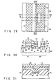
- FIGS. 11 to 13 show the main portion of a nonvolatile semiconductor memory device of the present invention.
- FIG. 11 is a plan view of the structure of a memory cell used in the nonvolatile semiconductor memory device of the invention.
- FIG. 12 is a sectional view taken along line XII-XII'.
- FIG. 13 is a sectional view taken along line XIII-XIII'.
- the memory cell is composed of a select MOS transistor ST and a data storage MOS transistor MT with a floating-gate electrode and a control gate electrode, these two transistor being connected to each other in series.
- Numeral 60 is a p-type silicon semiconductor substrate, for example.
- the surface region of the substrate 60 is made up of an SDG region (source, drain, and gate regions) and a field region.
- SDG region source, drain, and gate regions
- n-type regions 61, 62', 62, 63, 64, 65 and channel regions 69, 70 are formed.
- n-type regions 61, 62' constitute the drain region of the select MOS transistor ST.
- the n-type regions 62, 63, 64 constitute the source region of the select MOS transistor ST and the drain region of the storage MOS transistor MT. These n-type regions 62, 63, 64 are arranged continuously in a line.
- the n-type region 65 is the source region of the data storage MOS transistor MT.
- the impurity concentration in the n-type region 64 is set lower than that in the n-type region 63. For instance, the difference in impurity concentration between the n-type regions 63 and 64 is set at more than several times. Therefore, when the dosage of the n-type region 63 is approximately 5 ⁇ 10 13 cm -2 , the dosage of the n-type region 64 is set at approximately 1 ⁇ 10 13 cm -2 .
- the impurity concentration in the n-type region 62 is not limited to a specific value or a specific range. That is, even if the impurity concentration in the n-type region 62 takes any value, the memory cell operates properly. Since making the impurity concentration in the n-type region 62 equal to that in the n-type region 64 enables the n-type region 62 and the n-type region 64 to be formed simultaneously, this helps reduce the number of manufacturing processes.
- a very thin silicon oxide film 66 of nearly 10 nm in thickness is formed on a part of the substrate where area A indicated by a dot-dash line overlaps with the SDG region as shown in FIG. 11, a very thin silicon oxide film 66 of nearly 10 nm in thickness is formed.
- the silicon oxide film 66 is formed on the most surface or the entire surface of the n-type region 63, on the n-type region 64, and on the substrate 60 between the n-type region 64 and the n-type region 65 (on the channel region 70 of the data storage MOS transistor MT).
- the silicon oxide film 66 serves not only as a path through which electrons pass during a write operation or an erase operation, but also as a gate insulating film of the data storage MOS transistor MT.
- a silicon oxide film 68 of several tens nm in thickness is formed on the remaining area of the SDG region where the silicon oxide film 66 has not been formed.
- the silicon oxide film 68 functions as a gate oxide film of the select MOS transistor ST.
- the floating-gate electrode 71 is formed into a shape with a slit-like opening in its center.
- the floating-gate electrode 71 is made up of a first portion 71A and a second portion 71B.
- the first portion 71A and the second portion 71B are electrically connected to each other on the field region.
- the thin silicon oxide film 66 is formed at least on a part of the substrate 60 where the SDG region overlaps with the first and second portions 71A, 71B of the floating-gate electrode. Only the silicon oxide film 66 directly under the first portion 71A of the floating-gate electrode acts as a tunnel insulating film, whereas only the silicon oxide film 66 directly under the second portion 71B of the floating-gate electrode acts as a gate insulating film.
- the silicon oxide film 68 of nearly several tens nm in thickness and a gate electrode 72 made of polysilicon are formed.
- an insulating film 74 of several tens nm in thickness and a control gate electrode 75 made of polysilicon are formed.
- the insulating film 74 consists of a silicon oxide film, a silicon nitride film, or a laminate film of these films (e.g., an ONO film), for example. It is preferable that the shape of the control gate electrode 75 should be almost equal to the shape of the floating-gate electrode 71 in the direction in which the drain and source are arranged.
- an insulating film 74 and a gate electrode 73 made of polysilicon are formed on and above the gate electrode 72 of the select MOS transistor ST.
- the gate electrode 72 and the gate electrode 73 are electrically connected to each other.
- the gate electrode 72 virtually functions as the gate electrode of the select MOS transistor ST.
- the reason why the select MOS transistor ST has a double-layered gate electrode is to form the floating-gate electrode and control electrode of the data storage MOS transistor MT and the gate electrode of the select MOS transistor ST in the same process at the same time.
- the two-layered gate electrode of the select MOS transistor ST has the effect of simplifying the manufacturing processes. It should be noted that even if the gate electrode of the select MOS transistor ST is designed to have a single-layer structure, the memory cell will operate properly.
- the dimension along the channel length of the data storage MOS transistor MT is determined by the sum of the following:
- the dimension is determined by the sum of a, d, and e.
- the n-type region 64 and n-type region 65 that determine the channel length of the data storage MOS transistor MT are formed in a self-aligning manner using the floating-gate electrode 71 and control gate electrode 75 as a mask. Therefore, with the invention, the problem with the conventional device of FIGS. 1 and 2 can be avoided. Specifically, it is not necessary to take into account the misalignment of the mask for forming the n-type region (source region) 65 of the data storage MOS transistor MT from the mask for forming the floating-gate electrode 71. Therefore, the memory cell can be made smaller by the amount of mask misalignment.
- the thickness of the gate oxide film of the data storage MOS transistor MT in the conventional devices in FIGS. 1 and 2 and FIGS. 4 and 5 is nearly several tens nm, whereas the thickness of the gate oxide film of the data storage MOS transistor MT in the memory cell in FIGS. 11 to 13 is nearly 10 nm.
- the channel length can be theoretically made several times shorter than that in the conventional device of FIGS. 1 and 2 or of FIGS. 4 and 5. Namely, since the channel length which accounts for the largest percentage of the factors determining the dimension along the channel length of the data storage MOS transistor MT, can be reduced, the area of the memory cell can be made much smaller.
- the width of the SDG region can be made smaller by the amount of mask misalignment.
- the spacing between adjacent SDG regions is determined by the withstand voltage between them. Therefore, reducing the dimension of the memory cell across the channel width decreases the spacing between adjacent SDG regions, thereby contributing to high integration of memory cells.
- the floating-gate electrode 71B since above the edge of the n-type region 64, the floating-gate electrode 71B exists, a substrate current develops.
- the impurity concentration in the n-type region 64 is much lower than that in the n-type region 63 (several times lower than the latter). Accordingly, the curve of the band at the edge of the n-type region 64 at the surface of the substrate is gentle, with the result that a substrate current due to band-to-band tunneling is very small.
- the depletion layer at the surface of the n-type region 63 can be prevented from expanding. This makes larger the effective electric field between the drain region and the floating-gate electrode, resulting in an increase in the write current due to the tunnel effect. As a result, the writing or erasing of data can be effected easily.
- the write current depends on the impurity concentration in the n-type region 63, the write current will not decrease even if the impurity concentration in the n-type region 64 is made lower.
- the impurity concentration in the n-type region 63 and that in the n-type region 64 can be set at the respective optimum values. Furthermore, by setting the impurity concentration in the n-type regions 63 and 64 at the optimum values, the drain voltage at which a write current starts to flow can be set lower than the drain voltage at which a substrate current starts to flow.
- drain voltage V D write current I R
- substrate current I S substrate current I S in the data storage MOS transistor MT.
- the impurity concentration in the n-type regions 63 and 64 at the optimum values, almost no substrate current is allowed to flow during a write operation.
- the write current I R first flows from the drain region 63 to the floating-gate electrode 71 by the FN tunnel effect.
- the write current I R and substrate current Is depend only on the impurity concentration in the drain region (n-type region) 52.
- the increase of the impurity concentration in the drain region 52 increases both the write current IR and the substrate current Is, whereas the decrease of the impurity concentration in the drain region 52 decreases both the write current I R and the substrate current Is.
- the ratio of the write current I R to the substrate current Is hardly changes with respect to the drain voltage V D .
- the drain voltage V D at which the write current IR starts to flow is higher than the drain voltage V D at which the substrate current Is starts to flow. Therefore, as the drain voltage V D is raised, the substrate current Is first starts to flow.
- the substrate voltage reaches the voltage at which the substrate current Is balances with the current supplied from the internal step-up circuit, the rise of the drain voltage V D stops.
- the substrate current Is during a write operation can be reduced to almost zero. Furthermore, not only an internal step-up operation but also a low power-consuming operation can be performed, thereby realizing a highly reliable memory cell.
- the floating-gate electrodes 71A and 71B are connected to each other in the field regions on the right and left sides of the SDG region.
- the floating-gate electrodes 71A and 71B may be connected to each other in the field region only on one side of the SDG region.
- the floatinggate electrode is formed into a U shape.
- a field oxide film 76 is formed on a p-type silicon substrate 60, and a SDG region and a field region are set.
- a silicon oxide film (not shown) formed on the SDG region.
- n-type impurities are implanted into the substrate 60 to form a n-type region 63 in the region where area B overlaps with the SDG region.
- the silicon oxide film is removed.
- a silicon oxide film 68 of nearly several tens nm in thickness is formed on the entire surface of the SDG region of the substrate 60. Thereafter, using a mask with an opening in area A enclosed by a dot-dash line, the silicon oxide film 68 in the region where area A overlaps with the SDG region, is removed. On the region of the substrate where the silicon oxide film 68 has been removed, another thin silicon oxide film 66 of approximately 10 nm in thickness is formed.
- a first polysilicon layer 71' is deposited on the entire surface of the substrate 60. Then, using a mask with a slit-like opening in area C enclosed by a dot-dash line, the first polysilicon layer is selectively removed.
- an insulating film 74 of nearly several tens nm in thickness is formed on the entire surface of the substrate 60. Then, on the insulating film 74, a second polysilicon layer 75' is deposited.
- the second polysilicon layer 75', the insulating film 74, and the first polysilicon layer 71' are etched consecutively to form floating-gate electrodes 71A, 71B, a control gate electrode 75, and two layers of gate electrodes 72, 73 for each memory cell in a selfaligning manner.
- n-type impurities are implanted into the substrate 60 to form n-type regions 62, 62', 64 in a self-aligning manner. At this time, the n-type regions 62, 64 are connected to the n-type region previously formed.
- n-type impurities are implanted into the substrate 60 to form n-type regions 61, 65.
- the n-type regions 62, 62', 64 are formed simultaneously in a self-aligning manner. This not only reduces the number of manufacturing processes, but also eliminates the necessity of taking mask misalignment into account. Furthermore, in the method, the impurity concentration in the n-type regions 62, 62' is equal to that in the n-type region 64. If it is desired that the impurity concentration in the n-type regions 62, 62' differ from that in the n-type region 64, the n-type regions 62, 62' have only to be formed independently from the n-type region 64, using a specific mask.
- FIG. 32 is a detail sectional view taken along line XIII-XIII' of FIG. 11.
- the very thin silicon oxide film 66 is formed on the entire surface of the SDG region overlapping with the floating-gate electrode 71.
- n-type region 63 is formed of only n-type impurities of a single type, the following drawback will arise:
- n-type region 63 is formed of only n-type impurities of a single type, the end of the drain region across the channel width of the data storage MOS transistor MT will be positioned directly under the very thin silicon oxide film 66.
- a depletion layer at the end of the drain region 63 expands as shown in FIG. 32, allowing a substrate current Is to flow by band-to-band tunneling at the end of the drain region 63 or at the boundary between the SDG region and the field region.
- the n-type region 63 is formed of n-type impurities of more than two types whose diffusion coefficient differs from each other, for example, arsenic (As), whose diffusion coefficient is low, and phosphorus (P), whose diffusion coefficient is high.
- As arsenic
- P phosphorus
- FIG. 33 a sectional view taken along line XIII-XIII' of FIG. 11 is given in FIG. 33.
- the end of the n-type region 63' formed of n-type impurities whose diffusion coefficient is high is positioned directly under the very thick field oxide film 76.
- the impurity concentration at the surface necessary for the drain region of the data storage MOS transistor MT is maintained by n-type impurities whose diffusion coefficient is low, and the position of the end of the drain region is controlled by n-type impurities whose diffusion coefficient is high. Therefore, the write characteristics can be improved by using n-type impurities whose diffusion coefficient is low, and a substrate current can be prevented using n-type impurities whose diffusion coefficient is high.
- n-type impurities of a single type whose diffusion coefficient is high e.g., phosphorus
- an attempt to optimize the impurity concentration at the surface of the drain region permits the drain region to penetrate the channel portion of the data storage MOS transistor, for example.
- An attempt to limit the extension of the drain region due to diffusion lowers the impurity concentration at the surface of the drain region, resulting in an insufficient write current.
- the method of manufacturing nonvolatile semiconductor memory devices according to the invention produces the following effects.
- both the channel length and the channel width can be shortened as compared with those of a conventional equivalent. As a result, the memory cell area can be made smaller.
- the drain region of the data storage MOS transistor is composed of an n-type region whose impurity concentration is high, and an n-type region whose impurity concentration is more than several times lower than the high impurity concentration in the preceding n-type region.
- the drain region of the data storage MOS transistor On the end of the channel length of the n-type region whose impurity concentration is high, there is a slit-like opening and therefore no floating-gate electrode exists above the end.
- a field oxide film is located on the end of the channel width.
Landscapes
- Non-Volatile Memory (AREA)
- Semiconductor Memories (AREA)
Claims (14)
- Nichtflüchtige Halbleiterspeichervorrichtung, die folgendes aufweist:ein Halbleitersubstrat (60) eines ersten Leitfähigkeitstyps mit einem Elementenbereich;einen Auswahl-MOS-Transistor (ST), der im Elementenbereich ausgebildet ist;einen Datenspeicherungs-MOS-Transistor (MT), der im Elementenbereich ausgebildet ist und der einen Sourcebereich (65) eines zweiten Leitfähigkeitstyps enthält, einen Drainbereich (62, 63, 64) eines zweiten Leitfähigkeitstyps, eine Floating-Gateelektrode (71A, 71B) und eine Steuergateelektrode (75), wobei die Floating-Gateelektrode aus einem ersten Teil (71A) über dem Drainbereich und einem zweiten Teil (71B) über dem Halbleitersubstrat zwischen dem Sourcebereich und dem Drainbereich zusammengesetzt ist, wobei der erste und der zweite Teil mit einem isolierenden Film (66) verbunden sind, der dünner als ein Gate-Isolierfilm (68) des Auswahl-MOS-Transistors ist, der zwischen dem Drainbereich und dem ersten Teil und zwischen dem Halbleitersubstrat und dem zweiten Teil angeordnet ist und wobei der erste Teil und der zweite Teil vom Elementenbereich beabstandet sind, wobei der Drainbereich des Datenspeicherungs-MOS-Transistors folgendes enthält:einen ersten Bereich (63), der in einem Bereich direkt unter dem ersten Teil angeordnet ist und sich zu dem Raum zwischen dem ersten Teil und dem zweiten Teil erstreckt; undeinen zweiten Bereich (64), von welchem ein Ende auf der Seite des zweiten Teils angeordnet ist und von welchem das andere Ende mit einem Ende des ersten Bereichs verbunden ist, und dessen Störstellenkonzentration mehr als mehrere Male niedriger als die Störstellenkonzentration im ersten Bereich ist.
- Nichtflüchtige Halbleiterspeichervorrichtung nach Anspruch 1, dadurch gekennzeichnet, daß der Drainbereich des Datenspeicherungs-MOS-Transistors weiterhin einen dritten Bereich (62) enthält, von welchem ein Ende mit dem anderen Ende des ersten Bereichs verbunden ist und von welchem das andere Ende auf der Seite einer Gateelektrode des Auswahl-MOS-Transistors angeordnet ist.
- Nichtflüchtige Halbleiterspeichervorrichtung nach Anspruch 2, dadurch gekennzeichnet, daß die Störstellenkonzentration im zweiten Bereich gleich der Störstellenkonzentration im dritten Bereich ist.
- Nichtflüchtige Halbleiterspeichervorrichtung nach Anspruch 3, dadurch gekennzeichnet, daß der erste, der zweite und der dritte Bereich auch als Sourcebereich des Auswahl-MOS-Transistors funktionieren.
- Nichtflüchtige Halbleiterspeichervorrichtung nach Anspruch 4, dadurch gekennzeichnet, daß die Störstellenkonzentration im ersten Bereich und im zweiten Bereich so eingestellt sind, daß dann, wenn ein positives Potential an einen Drainbereich des Datenspeicherungs-MOS-Transistors angelegt wird und ein Erdpotential an die Steuergateelektrode, ein Strom freigegeben wird, um vom Drainbereich des Datenspeicherungs-MOS-Transistors zur Floating-Gateelektrode zu fließen, bevor ein Strom beginnt, vom Drainbereich des Datenspeicherungs-MOS-Transistors zum Substrat zu fließen.
- Nichtflüchtige Halbleiterspeichervorrichtung nach Anspruch 1, dadurch gekennzeichnet, daß
der erste Bereich (63) folgendes aufweist:eine erste Diffusionsschicht, die erste Störstellen eines zweiten Leitfähigkeitstyps enthält und einen Rand bzw. eine Kante hat, der bzw. die genau unter dem Isolierbereich angeordnet ist; undeine zweite Diffusionsschicht, die zweite Störstellen des zweiten Leitfähigkeitstyps mit einem Diffusionskoeffizienten enthält, der kleiner als ein Diffusionskoeffizient der ersten Störstellen ist. - Nichtflüchtige Halbleiterspeichervorrichtung nach Anspruch 6, dadurch gekennzeichnet, daß die Störstellen von mehr als zwei Typen, deren Diffusionskoeffizienten unterschiedlich voneinander sind, Arsen und Phosphor enthalten.
- Nichtflüchtige Halbleiterspeichervorrichtung nach Anspruch 1, dadurch gekennzeichnet, daß der Isolierfilm zwischen dem Drainbereich und dem ersten Teil als Tunnel-Isolierfilm funktioniert, der zuläßt, daß ein Fowler-Nordheim-Tunnelstrom stattfindet, und der Isolierfilm zwischen dem Halbleitersubstrat und dem zweiten Teil als Gate-Isolierfilm des Datenspeicherungs-MOS-Transistors und als Tunnel-Isolierfilm funktioniert.
- Nichtflüchtige Halbleiterspeichervorrichtung nach Anspruch 1, dadurch gekennzeichnet, daß der Isolierfilm zwischen dem Drainbereich und dem ersten Teil und derjenige zwischen dem Halbleitersubstrat und dem zweiten Teil eine Dicke von nahezu 10 nm haben, und der Gate-Isolierfilm des Auswahl-MOS-Transistors eine Dicke von mehreren Zehn nm hat.
- Nichtflüchtige Halbleiterspeichervorrichtung nach Anspruch 1, dadurch gekennzeichnet, daß im Elementenbereich die Form der Steuergateelektrode dieselbe wie diejenige der Floating-Gateelektrode ist.
- Verfahren zum Herstellen einer nichtflüchtigen Halbleiterspeichervorrichtung, die einen Auswahl-MOS-Transistor (ST) und einen Datenspeicherungs-MOS-Transistor (MT) auf einem Halbleitersubstrat (60) eines ersten Leitfähigkeitstyps enthält, wobei das Halbleitersubstrat einen Elementenbereich aufweist, wobei das Verfahren die folgenden Schritte aufweist:Ausbilden eines ersten Bereichs (63) durch Implantieren von Störstellen eines zweiten Leitfähigkeitstyps in einen beschränkten Bereich des Elementenbereichs des Halbleitersubstrats;Ausbilden eines ersten Isolierfilms (68) im Elementenbereich;Entfernen des ersten Isolierfilms im ersten Bereich und in einem Bereich, der in einer ersten Richtung benachbart zum ersten Bereich ist;Ausbilden eines zweiten Isolierfilms (66), der dünner als der erste Isolierfilm ist, auf dem Halbleitersubstrat, das im Elementenbereich durch den Entfernungsschritt freigelegt ist;Ausbilden eines ersten leitenden Films (71') auf der gesamten Oberfläche des Halbleitersubstrats;Ausbilden eines schlitzartigen Lochs (C) im ersten leitenden Film bei einer Position, die in einer zweiten Richtung, die orthogonal zur ersten Richtung ist, jeweils von dem Bereich beabstandet ist, der durch den Schritt zum Ausbilden des zweiten Isolierfilms definiert ist;Ausbilden eines dritten Isolierfilms (74) auf der gesamten Oberfläche des Halbleitersubstrats;Ausbilden eines zweiten leitenden Films (75') auf dem dritten Isolierfilm;Ätzen des zweiten leitenden Films, des dritten Isolierfilms, des ersten leitenden Films, des zweiten Isolierfilms und des ersten Isolierfilms in Aufeinanderfolge, um eine Gateelektrode (72, 73) des Auswahl-MOS-Transistors und eine Steuergateelektrode (71A, 71B) und eine Floating-Gateelektrode (75) des Datenspeicherungs-MOS-Transistors auszubilden, wobei die Steuergateelektrode und die Floating-Gateelektrode einen ersten Teil (71) und einen zweiten Teil (71B) über dem Elementenbereich haben, wobei der erste Teil über dem ersten Bereich angeordnet ist, und wobei der erste Teil und der zweite Teil auf dem Elementenbereich beabstandet sind; undImplantieren von Störstellen eines zweiten Leitfähigkeitstyps in den Elementenbereich mit der Gateelektrode des Auswahl-MOS-Transistors und der Steuergateelektrode und der Floating-Gateelektrode des Datenspeicherungs-MOS-Transistors als Maske, um einen zweiten Bereich (64) im Elementenbereich zwischen dem ersten Teil und dem zweiten Teil und einen dritten Bereich (62) im Elementenbereich zwischen dem ersten Teil und der Gateelektrode des Auswahl-MOS-Transistors auszugeben, wobei der zweite Bereich (64) eine Störstellenkonzentration hat, die mehr als mehrere Male niedriger als die Störstellenkonzentration im ersten Bereich (63) ist.
- Verfahren nach Anspruch 11, dadurch gekennzeichnet, daß der zweite und der dritte Bereich so ausgebildet werden, daß die Störstellenkonzentration im dritten Bereich (62) niedriger als im ersten Bereich (63) ist.
- Verfahren nach Anspruch 11, dadurch gekennzeichnet, daß der erste, der zweite und der dritte Bereich (62, 63, 64) so ausgebildet werden, um als der Sourcebereich des Auswahl-MOS-Transistors zu funktionieren, zusätzlich zum Funktionieren als der Drainbereich des Datenspeicherungs-MOS-Transistors.
- Verfahren nach Anspruch 11, dadurch gekennzeichnet, daß der erste Bereich (63) durch Implantieren von Störstellen von mehr als zwei Typen, deren Diffusionskoeffizienten voneinander unterschiedlich sind, im Elementenbereich ausgebildet wird.
Applications Claiming Priority (3)
| Application Number | Priority Date | Filing Date | Title |
|---|---|---|---|
| JP29995193 | 1993-11-30 | ||
| JP29995193 | 1993-11-30 | ||
| JP299951/93 | 1993-11-30 |
Publications (3)
| Publication Number | Publication Date |
|---|---|
| EP0655785A2 EP0655785A2 (de) | 1995-05-31 |
| EP0655785A3 EP0655785A3 (de) | 1995-11-22 |
| EP0655785B1 true EP0655785B1 (de) | 2001-10-17 |
Family
ID=17878932
Family Applications (1)
| Application Number | Title | Priority Date | Filing Date |
|---|---|---|---|
| EP94118861A Expired - Lifetime EP0655785B1 (de) | 1993-11-30 | 1994-11-30 | Nichtflüchtige Halbleiterspeicheranordnung und Verfahren zur Herstellung |
Country Status (4)
| Country | Link |
|---|---|
| US (3) | US5596529A (de) |
| EP (1) | EP0655785B1 (de) |
| KR (1) | KR0147452B1 (de) |
| DE (1) | DE69428658T2 (de) |
Families Citing this family (34)
| Publication number | Priority date | Publication date | Assignee | Title |
|---|---|---|---|---|
| KR0142604B1 (ko) * | 1995-03-22 | 1998-07-01 | 김주용 | 플래쉬 이이피롬 셀 및 그 제조방법 |
| KR100413652B1 (ko) * | 1995-09-11 | 2004-05-27 | 마츠시타 덴끼 산교 가부시키가이샤 | 반도체기억장치및그구동방법 |
| US6162682A (en) * | 1995-09-29 | 2000-12-19 | Cypress Semiconductor Corporation | Structure and process for a gouge-free stacked non-volatile memory cell with select gate |
| JP2910647B2 (ja) * | 1995-12-18 | 1999-06-23 | 日本電気株式会社 | 不揮発性半導体記憶装置の製造方法 |
| EP0782196A1 (de) * | 1995-12-28 | 1997-07-02 | STMicroelectronics S.r.l. | Herstellungsverfahren für EEPROM-Speicherbauelemente und dadurch hergestellte EEPROM-Speicherbauelemente |
| DE19614011C2 (de) | 1996-04-09 | 2002-06-13 | Infineon Technologies Ag | Halbleiterbauelement, bei dem die Tunnelgateelektrode und die Kanalgateelektrode an der Grenzfläche zum Tunneldielektrikum bzw. Gatedielektrikum durch eine Isolationsstruktur unterbrochen sind |
| JPH104149A (ja) * | 1996-06-14 | 1998-01-06 | Oki Electric Ind Co Ltd | 半導体記憶装置および製造方法 |
| US5761120A (en) * | 1996-08-27 | 1998-06-02 | Peng; Jack Zezhong | Floating gate FPGA cell with select device on drain |
| US5963824A (en) * | 1997-07-09 | 1999-10-05 | Advanced Micro Devices, Inc. | Method of making a semiconductor device with adjustable threshold voltage |
| JPH11297860A (ja) * | 1998-03-26 | 1999-10-29 | Newcore Technol Inc | 半導体記憶装置 |
| US6114724A (en) * | 1998-03-31 | 2000-09-05 | Cypress Semiconductor Corporation | Nonvolatile semiconductor memory cell with select gate |
| DE69836423D1 (de) * | 1998-06-30 | 2006-12-28 | St Microelectronics Srl | Verfahren zur Herstellung einer EEPROM-Speicherzelle |
| DE19929618B4 (de) * | 1999-06-28 | 2006-07-13 | Infineon Technologies Ag | Verfahren zur Herstellung einer nichtflüchtigen Halbleiter-Speicherzelle mit separatem Tunnelfenster |
| EP1071134A1 (de) * | 1999-07-22 | 2001-01-24 | STMicroelectronics S.r.l. | Verfahren zur Herstellung eines Halbleiterbauelementes mit EEPROM-Speicherzellen unter Kontrolle der Abmessungen der Floating-Gate-Gebiete |
| FR2800200B1 (fr) * | 1999-10-21 | 2002-01-04 | St Microelectronics Sa | Procede de fabrication de points memoire eeprom |
| DE10235072A1 (de) * | 2002-07-31 | 2004-02-26 | Micronas Gmbh | EEPROM-Struktur für Halbleiterspeicher |
| US6900502B2 (en) * | 2003-04-03 | 2005-05-31 | Taiwan Semiconductor Manufacturing Company, Ltd. | Strained channel on insulator device |
| US6882025B2 (en) * | 2003-04-25 | 2005-04-19 | Taiwan Semiconductor Manufacturing Company, Ltd. | Strained-channel transistor and methods of manufacture |
| US6867433B2 (en) * | 2003-04-30 | 2005-03-15 | Taiwan Semiconductor Manufacturing Company, Ltd. | Semiconductor-on-insulator chip incorporating strained-channel partially-depleted, fully-depleted, and multiple-gate transistors |
| US6936881B2 (en) * | 2003-07-25 | 2005-08-30 | Taiwan Semiconductor Manufacturing Company, Ltd. | Capacitor that includes high permittivity capacitor dielectric |
| US7078742B2 (en) | 2003-07-25 | 2006-07-18 | Taiwan Semiconductor Manufacturing Co., Ltd. | Strained-channel semiconductor structure and method of fabricating the same |
| US6940705B2 (en) * | 2003-07-25 | 2005-09-06 | Taiwan Semiconductor Manufacturing Company, Ltd. | Capacitor with enhanced performance and method of manufacture |
| US7101742B2 (en) * | 2003-08-12 | 2006-09-05 | Taiwan Semiconductor Manufacturing Company, Ltd. | Strained channel complementary field-effect transistors and methods of manufacture |
| US7112495B2 (en) * | 2003-08-15 | 2006-09-26 | Taiwan Semiconductor Manufacturing Company, Ltd. | Structure and method of a strained channel transistor and a second semiconductor component in an integrated circuit |
| US20050035410A1 (en) * | 2003-08-15 | 2005-02-17 | Yee-Chia Yeo | Semiconductor diode with reduced leakage |
| US7071052B2 (en) * | 2003-08-18 | 2006-07-04 | Taiwan Semiconductor Manufacturing Company, Ltd. | Resistor with reduced leakage |
| US7888201B2 (en) | 2003-11-04 | 2011-02-15 | Taiwan Semiconductor Manufacturing Company, Ltd. | Semiconductor-on-insulator SRAM configured using partially-depleted and fully-depleted transistors |
| US8558278B2 (en) | 2007-01-16 | 2013-10-15 | Taiwan Semiconductor Manufacturing Company, Ltd. | Strained transistor with optimized drive current and method of forming |
| US7821061B2 (en) | 2007-03-29 | 2010-10-26 | Intel Corporation | Silicon germanium and germanium multigate and nanowire structures for logic and multilevel memory applications |
| US7800156B2 (en) * | 2008-02-25 | 2010-09-21 | Tower Semiconductor Ltd. | Asymmetric single poly NMOS non-volatile memory cell |
| US7859043B2 (en) * | 2008-02-25 | 2010-12-28 | Tower Semiconductor Ltd. | Three-terminal single poly NMOS non-volatile memory cell |
| US8344440B2 (en) * | 2008-02-25 | 2013-01-01 | Tower Semiconductor Ltd. | Three-terminal single poly NMOS non-volatile memory cell with shorter program/erase times |
| US7943961B2 (en) * | 2008-03-13 | 2011-05-17 | Taiwan Semiconductor Manufacturing Company, Ltd. | Strain bars in stressed layers of MOS devices |
| US7808051B2 (en) * | 2008-09-29 | 2010-10-05 | Taiwan Semiconductor Manufacturing Company, Ltd. | Standard cell without OD space effect in Y-direction |
Family Cites Families (13)
| Publication number | Priority date | Publication date | Assignee | Title |
|---|---|---|---|---|
| JPS6252973A (ja) * | 1985-08-30 | 1987-03-07 | Mitsubishi Electric Corp | 半導体記憶装置 |
| US4804637A (en) * | 1985-09-27 | 1989-02-14 | Texas Instruments Incorporated | EEPROM memory cell and driving circuitry |
| JPS6294987A (ja) * | 1985-10-21 | 1987-05-01 | Nec Corp | Mis電界効果型半導体装置及びその情報の検出方法 |
| IT1191561B (it) * | 1986-06-03 | 1988-03-23 | Sgs Microelettrica Spa | Dispositivo di memoria non labile a semiconduttore con porta non connessa (floating gate) alterabile elettricamente |
| JPS6384168A (ja) * | 1986-09-29 | 1988-04-14 | Toshiba Corp | 不揮発性半導体記憶装置 |
| US5066992A (en) * | 1989-06-23 | 1991-11-19 | Atmel Corporation | Programmable and erasable MOS memory device |
| JP2807304B2 (ja) * | 1990-02-19 | 1998-10-08 | 株式会社東芝 | 不揮発性半導体装置 |
| US5282161A (en) * | 1990-12-31 | 1994-01-25 | Sgs-Thomson Microelectronics S.R.L. | Eeprom cell having a read interface isolated from the write/erase interface |
| US5297082A (en) * | 1992-11-12 | 1994-03-22 | Micron Semiconductor, Inc. | Shallow trench source eprom cell |
| US5432740A (en) * | 1993-10-12 | 1995-07-11 | Texas Instruments Incorporated | Low voltage flash EEPROM memory cell with merge select transistor and non-stacked gate structure |
| JPH07335883A (ja) * | 1994-06-15 | 1995-12-22 | Toshiba Corp | 半導体装置の製造方法 |
| KR0142601B1 (ko) * | 1995-02-28 | 1998-07-01 | 김주용 | 플래쉬 이이피롬 셀의 제조방법 |
| US5589413A (en) * | 1995-11-27 | 1996-12-31 | Taiwan Semiconductor Manufacturing Company | Method of manufacturing self-aligned bit-line during EPROM fabrication |
-
1994
- 1994-11-30 KR KR1019940032724A patent/KR0147452B1/ko not_active Expired - Lifetime
- 1994-11-30 US US08/351,185 patent/US5596529A/en not_active Expired - Lifetime
- 1994-11-30 DE DE69428658T patent/DE69428658T2/de not_active Expired - Lifetime
- 1994-11-30 EP EP94118861A patent/EP0655785B1/de not_active Expired - Lifetime
-
1996
- 1996-10-16 US US08/732,669 patent/US5702966A/en not_active Expired - Lifetime
- 1996-11-01 US US08/742,492 patent/US5844268A/en not_active Expired - Lifetime
Non-Patent Citations (1)
| Title |
|---|
| S.M. SZE: "High speed semiconductor devices", 1990, WILEY & SONS * |
Also Published As
| Publication number | Publication date |
|---|---|
| KR0147452B1 (ko) | 1998-08-01 |
| US5596529A (en) | 1997-01-21 |
| DE69428658T2 (de) | 2002-06-20 |
| US5844268A (en) | 1998-12-01 |
| DE69428658D1 (de) | 2001-11-22 |
| EP0655785A2 (de) | 1995-05-31 |
| US5702966A (en) | 1997-12-30 |
| EP0655785A3 (de) | 1995-11-22 |
| KR950015763A (ko) | 1995-06-17 |
Similar Documents
| Publication | Publication Date | Title |
|---|---|---|
| US5702966A (en) | Method of manufacturing a semiconductor memory device | |
| US5773343A (en) | Semiconductor device having a recessed channel structure and method for fabricating the same | |
| US5108939A (en) | Method of making a non-volatile memory cell utilizing polycrystalline silicon spacer tunnel region | |
| EP0676811A1 (de) | EEPROM-Zelle mit Isolationstransistor und Betriebs- und Herstellungsverfahren | |
| KR20010023706A (ko) | 비휘발성 메모리 셀 | |
| KR0144421B1 (ko) | 플레쉬 이.이.피.롬의 제조방법 | |
| US5463579A (en) | Semiconductor memory device with floating gate and method for driving the same | |
| US5338956A (en) | Electrically erasable and programmable read only memory having a thin film transferring transistor over a floating gate memory transistor | |
| JPH09283644A (ja) | フラッシュメモリーの構造および製造方法 | |
| EP0443515B1 (de) | Nichtflüchtige Halbleitervorrichtung | |
| US5461249A (en) | Nonvolatile semiconductor memory device and manufacturing method therefor | |
| US7166887B2 (en) | EEPROM device and method of fabricating the same | |
| EP0399527A2 (de) | Nichtflüchtige Halbleiter-Speichereinrichtung | |
| KR100276651B1 (ko) | 비휘발성반도체소자제조방법 | |
| JP2964636B2 (ja) | 不揮発性半導体記憶装置の製造方法 | |
| US5675163A (en) | Non-volatile semiconductor memory device with thin insulation layer below erase gate | |
| JP3222705B2 (ja) | 不揮発性半導体記憶装置及びその製造方法 | |
| KR100546382B1 (ko) | 커플링비를 향상시킬 수 있는 이이피롬 소자 및 그 제조방법 | |
| KR100734261B1 (ko) | 커플링비를 향상시킬 수 있는 비휘발성 반도체 메모리 소자 | |
| KR100215888B1 (ko) | 플래쉬 메모리 제조방법 | |
| JPH07112018B2 (ja) | 半導体記憶装置 | |
| KR960013510B1 (ko) | 플레쉬 메모리 및 그 제조방법 | |
| Amin | Design, selection and implementation of flash erase EEPROM memory cells | |
| US6153906A (en) | Flash memory | |
| JPH0730001A (ja) | 半導体装置 |
Legal Events
| Date | Code | Title | Description |
|---|---|---|---|
| PUAI | Public reference made under article 153(3) epc to a published international application that has entered the european phase |
Free format text: ORIGINAL CODE: 0009012 |
|
| 17P | Request for examination filed |
Effective date: 19941130 |
|
| AK | Designated contracting states |
Kind code of ref document: A2 Designated state(s): DE FR GB |
|
| PUAL | Search report despatched |
Free format text: ORIGINAL CODE: 0009013 |
|
| AK | Designated contracting states |
Kind code of ref document: A3 Designated state(s): DE FR GB |
|
| RIN1 | Information on inventor provided before grant (corrected) |
Inventor name: TOHYAMA, DAISUKE, C/O INTELLECTUAL PROPERTY DIV. Inventor name: NODA, JUNICHIRO, C/O INTELLECTUAL PROPERTY DIV. |
|
| 17Q | First examination report despatched |
Effective date: 19970220 |
|
| GRAG | Despatch of communication of intention to grant |
Free format text: ORIGINAL CODE: EPIDOS AGRA |
|
| GRAG | Despatch of communication of intention to grant |
Free format text: ORIGINAL CODE: EPIDOS AGRA |
|
| GRAH | Despatch of communication of intention to grant a patent |
Free format text: ORIGINAL CODE: EPIDOS IGRA |
|
| GRAH | Despatch of communication of intention to grant a patent |
Free format text: ORIGINAL CODE: EPIDOS IGRA |
|
| GRAA | (expected) grant |
Free format text: ORIGINAL CODE: 0009210 |
|
| AK | Designated contracting states |
Kind code of ref document: B1 Designated state(s): DE FR GB |
|
| REF | Corresponds to: |
Ref document number: 69428658 Country of ref document: DE Date of ref document: 20011122 |
|
| REG | Reference to a national code |
Ref country code: GB Ref legal event code: IF02 |
|
| ET | Fr: translation filed | ||
| PLBE | No opposition filed within time limit |
Free format text: ORIGINAL CODE: 0009261 |
|
| STAA | Information on the status of an ep patent application or granted ep patent |
Free format text: STATUS: NO OPPOSITION FILED WITHIN TIME LIMIT |
|
| 26N | No opposition filed | ||
| PGFP | Annual fee paid to national office [announced via postgrant information from national office to epo] |
Ref country code: GB Payment date: 20131127 Year of fee payment: 20 Ref country code: DE Payment date: 20131127 Year of fee payment: 20 Ref country code: FR Payment date: 20131108 Year of fee payment: 20 |
|
| REG | Reference to a national code |
Ref country code: DE Ref legal event code: R071 Ref document number: 69428658 Country of ref document: DE |
|
| REG | Reference to a national code |
Ref country code: DE Ref legal event code: R071 Ref document number: 69428658 Country of ref document: DE |
|
| REG | Reference to a national code |
Ref country code: GB Ref legal event code: PE20 Expiry date: 20141129 |
|
| PG25 | Lapsed in a contracting state [announced via postgrant information from national office to epo] |
Ref country code: GB Free format text: LAPSE BECAUSE OF EXPIRATION OF PROTECTION Effective date: 20141129 |