EP0656582B1 - Schaltung und Verfahren zur parallelen Addition und Mittelwertbildung - Google Patents
Schaltung und Verfahren zur parallelen Addition und Mittelwertbildung Download PDFInfo
- Publication number
- EP0656582B1 EP0656582B1 EP94112045A EP94112045A EP0656582B1 EP 0656582 B1 EP0656582 B1 EP 0656582B1 EP 94112045 A EP94112045 A EP 94112045A EP 94112045 A EP94112045 A EP 94112045A EP 0656582 B1 EP0656582 B1 EP 0656582B1
- Authority
- EP
- European Patent Office
- Prior art keywords
- word
- bit
- sub
- result
- bits
- Prior art date
- Legal status (The legal status is an assumption and is not a legal conclusion. Google has not performed a legal analysis and makes no representation as to the accuracy of the status listed.)
- Expired - Lifetime
Links
Images


Classifications
-
- G—PHYSICS
- G06—COMPUTING OR CALCULATING; COUNTING
- G06F—ELECTRIC DIGITAL DATA PROCESSING
- G06F7/00—Methods or arrangements for processing data by operating upon the order or content of the data handled
- G06F7/38—Methods or arrangements for performing computations using exclusively denominational number representation, e.g. using binary, ternary, decimal representation
- G06F7/48—Methods or arrangements for performing computations using exclusively denominational number representation, e.g. using binary, ternary, decimal representation using non-contact-making devices, e.g. tube, solid state device; using unspecified devices
- G06F7/50—Adding; Subtracting
- G06F7/505—Adding; Subtracting in bit-parallel fashion, i.e. having a different digit-handling circuit for each denomination
- G06F7/506—Adding; Subtracting in bit-parallel fashion, i.e. having a different digit-handling circuit for each denomination with simultaneous carry generation for, or propagation over, two or more stages
- G06F7/508—Adding; Subtracting in bit-parallel fashion, i.e. having a different digit-handling circuit for each denomination with simultaneous carry generation for, or propagation over, two or more stages using carry look-ahead circuits
-
- G—PHYSICS
- G06—COMPUTING OR CALCULATING; COUNTING
- G06F—ELECTRIC DIGITAL DATA PROCESSING
- G06F7/00—Methods or arrangements for processing data by operating upon the order or content of the data handled
- G06F7/38—Methods or arrangements for performing computations using exclusively denominational number representation, e.g. using binary, ternary, decimal representation
- G06F7/48—Methods or arrangements for performing computations using exclusively denominational number representation, e.g. using binary, ternary, decimal representation using non-contact-making devices, e.g. tube, solid state device; using unspecified devices
- G06F7/544—Methods or arrangements for performing computations using exclusively denominational number representation, e.g. using binary, ternary, decimal representation using non-contact-making devices, e.g. tube, solid state device; using unspecified devices for evaluating functions by calculation
-
- G—PHYSICS
- G06—COMPUTING OR CALCULATING; COUNTING
- G06F—ELECTRIC DIGITAL DATA PROCESSING
- G06F7/00—Methods or arrangements for processing data by operating upon the order or content of the data handled
- G06F7/38—Methods or arrangements for performing computations using exclusively denominational number representation, e.g. using binary, ternary, decimal representation
- G06F7/48—Methods or arrangements for performing computations using exclusively denominational number representation, e.g. using binary, ternary, decimal representation using non-contact-making devices, e.g. tube, solid state device; using unspecified devices
- G06F7/57—Arithmetic logic units [ALU], i.e. arrangements or devices for performing two or more of the operations covered by groups G06F7/483 – G06F7/556 or for performing logical operations
- G06F7/575—Basic arithmetic logic units, i.e. devices selectable to perform either addition, subtraction or one of several logical operations, using, at least partially, the same circuitry
-
- G—PHYSICS
- G06—COMPUTING OR CALCULATING; COUNTING
- G06F—ELECTRIC DIGITAL DATA PROCESSING
- G06F2207/00—Indexing scheme relating to methods or arrangements for processing data by operating upon the order or content of the data handled
- G06F2207/38—Indexing scheme relating to groups G06F7/38 - G06F7/575
- G06F2207/3804—Details
- G06F2207/3808—Details concerning the type of numbers or the way they are handled
- G06F2207/3812—Devices capable of handling different types of numbers
- G06F2207/382—Reconfigurable for different fixed word lengths
-
- G—PHYSICS
- G06—COMPUTING OR CALCULATING; COUNTING
- G06F—ELECTRIC DIGITAL DATA PROCESSING
- G06F2207/00—Indexing scheme relating to methods or arrangements for processing data by operating upon the order or content of the data handled
- G06F2207/38—Indexing scheme relating to groups G06F7/38 - G06F7/575
- G06F2207/3804—Details
- G06F2207/3808—Details concerning the type of numbers or the way they are handled
- G06F2207/3828—Multigauge devices, i.e. capable of handling packed numbers without unpacking them
-
- G—PHYSICS
- G06—COMPUTING OR CALCULATING; COUNTING
- G06F—ELECTRIC DIGITAL DATA PROCESSING
- G06F7/00—Methods or arrangements for processing data by operating upon the order or content of the data handled
- G06F7/38—Methods or arrangements for performing computations using exclusively denominational number representation, e.g. using binary, ternary, decimal representation
- G06F7/48—Methods or arrangements for performing computations using exclusively denominational number representation, e.g. using binary, ternary, decimal representation using non-contact-making devices, e.g. tube, solid state device; using unspecified devices
- G06F7/499—Denomination or exception handling, e.g. rounding or overflow
- G06F7/49942—Significance control
- G06F7/49947—Rounding
- G06F7/49963—Rounding to nearest
Definitions
- the present invention relates to computers, and more particularly, to arithmetic units for use therein.
- Computers normally include an arithmetic logic unit that includes an adder that adds numbers of some maximum number of bits.
- Adders for words of length 32 and 64 bits are common in microprocessors and the like. While these adders will also operate on much smaller words, when doing so, the majority of the logic circuits contained in the adders are idle.
- a 64-bit adder can be used to add two 8-bit words by placing each of the 8-bit words in the least significant portion of a corresponding 64-bit word and then adding the 64-bit words.
- the logic circuitry concerned with adding the 7 high order bytes of each of the words is effectively idle. Hence, 7/8 ths of the capacity of the adder is being wasted during this operation.
- the computer will normally have a 32-bit adder. During these computations, 75% of the adding capacity of the adder will be idle. Hence, a conventional arithmetic logic unit is not being used optimally when performing this type of image calculation.
- the image addition problem discussed above often includes generating an average image.
- An image having pixels that are the average of the corresponding pixels in the component images is equivalent to generating the pixels of the sum image discussed above and then dividing the intensity of each of the sum image pixels by 2. This type of image computation is preferred since it prevents overflows. If the two corresponding component image pixel values have values greater than 128, then the sum image pixel cannot be represented as an 8-bit integer. To avoid this problem, the average image is used, since the average image pixels will always be representable as one byte integers if the component image pixels were one byte integers.
- the present invention is an improved adder that can be configured to perform a plurality of partial word adds or averaging operations in parallel.
- an adder 10 accepts two N-bit operands 12 and 14.
- the operands are typically stored in two of the registers in the processor of the computer.
- the present invention could be implemented in forms of circuitry that are not included in computers.
- adder 10 When operated as a conventional adder, adder 10 generates an N bit output word 16 having the two's complement sum of X and Y and a 1-bit carry-out.
- the bits of output 16 of adder 10 will be denoted by Z i in the following discussion.
- the result of the addition is typically stored back into one of the CPU registers.
- bits in the various words will be numbered from least significant to most significant. That is, X 0 is the least significant bit of operand X, and X N-1 is the most significant bit of the X operand. The same convention will be used for the Y and Z words.
- the present invention allows each of the operands to be divided into a plurality of sub-words.
- the present invention will be explained first in terms of a single division of each of the operands into partial operands.
- the first k bits of the X operand, X 0 through X k-1 are the bits of the first partial operand 18 of the X word
- the remaining bits, X k through X N-1 are the bits of the second partial operand 17 of the X word.
- the Y operand is similarly divided into partial words 19 and 20.
- bits Z 0 through Z k-1 are the bits of the sum of partial operands 18 and 20, and bits Z k through Z N-1 are the bits of the sum of partial operands 17 and 19, respectively.
- bits Z 0 through Z k-1 are the bits of the average of partial operands 18 and 20, and bits Z k through Z N-1 are the bits of the average of partial operands 17 and 19, respectively.
- FIG. 2 is a block diagram of a portion of an adder 30 according to the present invention which only performs additions. That is, adder 30 does not perform averaging calculations.
- Adder 30 is constructed from an array of one bit adder stages.
- the present invention differs from a conventional adder in that the stages may be decoupled to allow the adder to perform parallel additions on the partial words.
- Each single bit adder adds two bits, one from the X operand and one from the Y operand, and a carry bit from the previous stage in the adder, denoted by C i for the i th stage, to generate a sum bit and a new carry bit.
- the two stages shown in Figure 2 are the single bit adders used to add the most significant bits of partial operands 18 and 20 and the least significant bits of partial operands 17 and 19.
- Single bit adder 31 for example, adds bits C k-2 , X k-1 and Y k-1 to generate sum bit S k-1 and carry bit C k-1 .
- the stage of the adder that adds bits X p and Y p to generate a sum bit S p will be referred to as the p th stage of the adder.
- the carry bit from each stage is propagated to the next stage by connecting the carry bit input of each stage to the carry bit output of the stage before it in the array of one bit adders.
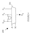
- the carry bit from the stage just before the boundary separating the two partial operands is connected to a blocking circuit 33.
- blocking circuit 33 connects the carry output of single bit adder 31 to the carry input of single bit adder 32.
- adder 30 is being used to perform two adds in parallel with partial word boundary between bits k-1 and k in each register, then blocking circuit 33 merely prevents the carry bit from single bit adder 31 from propagating to the carry input of single bit adder 32. This is accomplished in response to a 1-bit signal M k . The manner in which the bits M k are specified will be discussed in more detail below.
- the carry bit from the single bit adder operating on the most significant bit of the operands is used to detect overflows. If this feature is to be implemented for each of the partial operands, the carry bit from the most significant bit additions of each of the partial operands is connected to an appropriate overflow circuit.
- the carry bits are ORed together and the resultant bit used to detect an overflow. This bit can be used to trigger a trap on overflow or it may be ORed with the contents of a single bit register. In the later case, the program can check the contents of the register to determine if any operation since the last time the register was checked has resulted in an overflow.
- the present invention can be constructed from a conventional adder merely by including a blocking circuit such as blocking circuit 33 between each pair of stages that could span the boundary between two partial operands. If the X and Y inputs are to be divisible into an arbitrary number of partial operands of arbitrary size, then a blocking section is included between each pair of single bit adders.
- the blocking sections are configured by a mask having bits M k that specify the location of the most significant bit of each partial operand. This mask will be referred to as the boundary mask in the following discussion.
- the bits of the mask may be stored in a register in the adder or may be generated directly from the instruction being executed by the instruction decoding circuitry of the processor in which the adder is located.
- Blocking circuit 33 replaces the carry bit by 0 during an addition in which the adder is divided into sub-adders with a boundary at the blocking circuit. If the adder is to be also used for 2's complement subtractions in which the adder is likewise divided, the carry bit must be forced to be a 1 instead of a 0.
- Blocking circuit 33 shown in Figure 2 implements both additions and subtractions by providing an input F having a value of either "0" or "1". When a boundary is active at blocking circuit 33, the value of F is the value presented to the next stage. If the boundary is inactive, then blocking circuit 33 merely transmits the carry bit, C k-1 , to the next stage.
- the above-described embodiments of the present invention do not perform averaging computations. While these embodiments provide significant advantages over the prior art, the preferred embodiment of the present invention provides additional hardware that provides the capability of computing averages.
- the additional hardware required to perform averaging computations will now be discussed.
- the average of two operands is the sum of the two operands divided by two. A division by two is equivalent to shifting the sum of the two operands to the right by one bit. The least significant bit of the sum is lost.
- the most significant bit of the average is the carry output of the single bit adder operating on the most significant bit of the partial operands.
- stage adding the least significant bits of the partial operands discards its sum bit when performing an average computation.
- This type of stage will be referred to as a least significant bit stage in the following discussion.
- the stage adding the most significant bits of a partial operand must route the carry bit generated thereby to the most significant bit of the result, and its sum bit to the next most significant bit of the result in addition to breaking the carry propagation chain.
- This type of stage will be referred to as a most significant bit stage in the following discussion.
- Stages that add bits between the least and most significant bits must route their sum bits to a location one position to the right of the position used when the stages performed addition. That is, the i th stage routes its sum bit to Z i-1 .
- This type of stage will be referred to as an interior bit stage in the following discussion.
- each adder stage must be capable of functioning in at most two of the three roles described above.
- Stage (N-1) needs only perform as a most significant bit stage.
- stage 0 needs only to perform as a least significant bit stage. All other stages must be capable of operating as interior bit stages when the adder is used for full word additions.
- those stages that can become the most or least significant bit stages of a parallel sub-word add or average must be capable of switching to those configurations.
- Adder 100 is constructed from a plurality of 4-bit adding sections of which adding section 102 is exemplary. Adding section 102 operates on bits q through q+3 of the X and Y registers to generate sum bits S q through S q+3 .
- Each adding section is functionally equivalent to 4 of the single bit adders described above in that each adding section receives 4 bits from the X register, 4 bits from the Y register and generates the corresponding four sum bits.
- adding section 102 generates a carry bit C q+3 and receives carry bit C q-1 .
- Blocking circuits 110 and 112 are shown on each side of adding section 102.
- the i th sum bit, S i is routed to the i th output bit, Z i , of the adder.
- Each output line Z i is connected to a multiplexer.
- Multiplexers 122 and 123 are examples of such multiplexers.
- the second type of multiplexers are those that are connected to output lines that can either be an internal bit or a most significant bit of a result. Such a multiplexer is shown at 121. These multiplexers will be referred to as most significant bit multiplexers.
- a most significant bit multiplexer is a 3-to-1 multiplexer which operates in response to A and the mask bit that determines if the multiplexer is connected to a most significant bit of a result. If A is false, then a most significant bit multiplexer connects Z i to S i . If A is true and the mask bit is also true, then a most significant bit multiplexer connects Z i to C i , where C i is the carry bit generated by the stage that generated S i .
- the most significant bit multiplexer connects Z i to S i+1 . It should be noted that the multiplexer connected to Z N-1 is a most significant bit multiplexer in which a 2-to-1 multiplexer is sufficient, since this multiplexer can never be an interior multiplexer.
- the third type of multiplexers are those that are connected to output lines that can either be an internal bit or a least significant bit of a result. Such a multiplexer is shown at 124. These will be referred to as least significant bit multiplexers. If the result of the average operation is to be truncated, i.e., the bit shifted out is to be ignored in determining the result, a least significant bit multiplexer is the same as an internal bit multiplexer.
- While truncation may be used as a method of rounding the result of an integer divide by shifting right, it can cause undesirable problems that can be prevented by other forms of rounding.
- an image is to be reduced in size by averaging adjacent pixels in the image. That is, each group of 4 pixels is to be replaced by one pixel having a value equal to the average of the 4 pixels replaced.
- the image is represented by an IxI pixel array.
- the pixel reduction can be accomplished by averaging the odd and even rows in the array to generate an IxI/2 pixel array.
- the odd and even columns of this intermediate array are then averaged to generate the final (I/2)x(I/2) array.
- the final image will have different statistical properties than the original image. For example, the reduced image will have a lower average light intensity then the original array. It is often important that this type of artifact be avoided.
- the present invention provides a means for avoiding this type of biased rounding.
- round odd logic is used to prevent this biasing.
- the result is rounded to the nearest odd integer if a round off error is created by the right shift. If the answer is exact before rounding, no change is made.
- a round off error occurs whenever a 1 is shifted off the result. This occurs when the least significant bit before shifting is a "1". In this case, the least significant bit of the result is set to a "1". If the bit shifted out is a "0", then the result was exact even after the shift, and the least significant bit of the result is unaltered.
- the present invention utilizes round odd because a round odd system can be implemented by the addition of a single OR gate 131 to the multiplexer.
- the multiplexer selects the signal (S i+1 OR S i ) for connection to Z i when A is true and the mask bit indicates that the multiplexer in question is the least significant bit of a result.
- S i is connected to Z i .
- the multiplexer connects Z i to S i+1 .
- Multiplexer arrangement 200 is constructed from a 4-to-1 multiplexer 201. It is assumed that the multiplexer is connected to output line Z q in the following discussion. Multiplexer 201 either couples S q+1 , S q , C q or (S q+1 OR S q ) to Z q depending on the state of the average signal and mask bits. Since multiplexer 201 must function properly both as a least significant bit multiplexer or a most significant bit multiplexer, it must be able to determine the state of both M q and M q+1 .
- the present invention also improves the overall computational efficiency of many types of computation in which the data is packed into words at the beginning of the computation.
- the image size reduction problem discussed above as it would be carried out on a computer having a 32-bit word size. If each pixel is represented by a one byte integer, the image data will typically be packed into words to save storage space. Hence, each horizontal line in the image will be represented by I/4 32-bit words.
- a word containing 4 pixels of the odd numbered line can be input to the X register and the corresponding word from the even numbered line input to the Y register.
- the contents of the Z register can then be stored directly to memory as one packed word of the resultant image line. This operation can be carried out without having to unpack the individual bytes and repack the result.
- the present invention allows 4 pixels to be processed with a single add instruction and avoids the packing and unpacking instructions needed with conventional adders.
- the present invention automatically generates the average of the two pixels, thereby eliminating one shift operation after each add.
- the parallel sub-word add instruction is no more complex than a conventional full word add instruction.
- a conventional full word add the programmer specifies two registers having the operands and a third register to hold the result.
- the present invention likewise, requires only the specification of three registers. If only a few possible configurations of the adder in partial operand fields are possible, these configurations can be included in the add instruction and the instruction decode circuitry can then generate the corresponding mask bits. Hence, no additional instructions are needed to setup the adder.
- the add instruction could specify a plurality of registers to receive the sums, each sum being loaded in the least significant bits of the register.
- the result could be sent directly to locations other than register, e.g. memory or other functional units.
- the operands could originate from other functional units or memory.
- carry-look ahead architecture is used because it has smaller delays.
- carry look-ahead adders the carry generation circuitry produces a propagate and a generate signal corresponding to each bit of the adder. These signals may be used in a manner analogous to the carry bits described above to allow the adder to be broken into parallel sub-word adders. Consider the case in which the adder is to be divided such that stage k operates on the most significant bit of the sub-word result.
- a blocking circuit such as blocking circuit 33 shown in Figure 2 can be inserted into the carry generation logic such that the propagate bit and the generate bit are forced to the appropriate values depending on the type of operation, i.e., addition or subtraction, that is being performed.
- the blocking circuit does not alter the values of the propagate and generate bits corresponding to stage k.
Landscapes
- Engineering & Computer Science (AREA)
- Physics & Mathematics (AREA)
- General Physics & Mathematics (AREA)
- Theoretical Computer Science (AREA)
- Computational Mathematics (AREA)
- Mathematical Analysis (AREA)
- Pure & Applied Mathematics (AREA)
- Mathematical Optimization (AREA)
- Computing Systems (AREA)
- General Engineering & Computer Science (AREA)
- Complex Calculations (AREA)
- Advance Control (AREA)
Claims (10)
- Vorrichtung (10, 30, 100) zum Verarbeiten des Inhalts eines X-Wortes (12), welches Bits Xi aufweist, und eines Y-Wortes (14), welches Bits Yi aufweist, zum Erzeugen eines Ergebniswortes, welches Bits Zi aufweist, wobei i = 0 bis N-1, wobei Z0 das niedrigstwertige Bit des Ergebniswortes (16) ist und ZN-1 das höchstwertige Bit des Ergebniswortes ist, wobei die Vorrichtung Mittel zum Aufteilen (33, 110, 112) der X-, der Y- und der Ergebnisworte in mehrere Unterworte (17, 18, 19, 20, 21, 22) aufweist, wobei jeweils ein Unterwort der Y- und der Ergebnisworte jeweils einem Unterwort der X-Worte entspricht; und Addiermittel (31, 32, 102, 121-124) aufweist, welche abhängig von einem ersten Befehl (A = falsch) die Summe jedes X-Unterwortes und des entsprechenden Y-Unterwortes erzeugen, wobei das Ergebnis das entsprechende Unterwort des Ergebniswortes bestimmt, und abhängig von einem zweiten Befehl (A = wahr) die Summe geteilt durch Zwei jedes X-Unterwortes und des entsprechenden Y-Unterwortes erzeugen, wobei das Ergebnis das entsprechende Unterwort des Ergebniswortes bestimmt, wobei die Addiermittel eine Vielzahl Addierabschnitte (102) aufweisen, wobei jeder Addierabschnitt (102) Multiplexer (121-124) aufweist, die diesem zugeordnet sind, wobei die Multiplexer von dem ersten und dem zweiten Befehl (A) gesteuert werden, wobei die Multiplexer so konfiguriert sind, daß sie als ein Multiplexer des niedrigstwertigen Bits (124), ein Multiplexer der mittleren Bits (122, 123) oder ein Multiplexer des höchstwertigen Bits (121) arbeiten, wobei an jeder Unterwort-Grenze ein Multiplexer des höchstwertigen Bits (121) vorgesehen ist, um einen Übertrag der Summe zu dem entsprechenden Unterwort zurückzuverschieben.
- Vorrichtung nach Anspruch 1, wobei der Multiplexer des höchstwertigen Bits (121) abhängig von einem dritten Signal (Mq+4) so konfiguriert wird, daß er einen Übertrag, der von dem Addierabschnitt (102) erzeugt wird, zu dem entsprechenden Unterwort des Ergebniswortes führt.
- Vorrichtung nach Anspruch 1 oder 2, wobei der Multiplexer des niedrigstwertigen Bits (124) abhängig von einem vierten Signal (Mq) so konfiguriert wird, daß er das niedrigstwertige Bit des entsprechenden Unterwortes des Ergebniswortes unterdrückt.
- Vorrichtung nach einem der vorangehenden Ansprüche, wobei die Vorrichtung Mittel zum Verarbeiten eines oder mehrerer Bits des X-Wortes und entsprechender Bits, die von dem Y-Wort abgeleitet werden, aufweist, sowie Mittel zum Erzeugen eines Erzeugungs-Bits und eines Fortpflanzungs-Bits, die jedem Bit des X-Wortes entsprechen, und wobei die Aufteilungsmittel Mittel zum Einstellen des Erzeugungs-Bits und des Fortpflanzungs-Bits auf solche Werte aufweist, die von der durchgeführten Verarbeitung bestimmt werden, wenn das Bit des X-Wortes das höchstwertige Bit eines Unterwortes ist.
- Vorrichtung nach einem der vorangehenden Ansprüche, wobei die Vorrichtung mehrere Addierstufen (31, 32, 102) aufweist, die in Reihe geschaltet sind, wobei jede Addierstufe Mittel zum Verarbeiten eines oder mehrerer Bits von dem X-Wort und entsprechender Bits, die von dem Y-Wort abgeleitet werden, aufweist sowie Mittel zum Fortpflanzen eines Übertrag-Bits der Addierstufe zu der nächsten Addierstufe in der Reihenschaltung, und wobei die Aufteilungsmittel Mittel (33, 110, 112) zum Einstellen des Übertrag-Bits auf einen Wert aufweisen, der durch die Verarbeitung bestimmt wird, die durchgeführt wird, wenn die Addierstufen Bits verschiedener Unterworte in dem X-Wort verarbeiten.
- Vorrichtung nach Anspruch 5, wobei die Addierstufen N Ergebnis-Bits Si, für i = 0 bis N-1 erzeugen, wobei Si aus der Verarbeitung von Xi abgeleitet wird, und wobei die Vorrichtung ferner N Multiplexer (121-124) aufweist, wobei jeder Multiplexer ein Signal erzeugt, das eines der Ergebnis-Bits anzeigt, wobei jeweils ein Multiplexer für jedes Ergebnis-Bit Zp, für p = 0 bis N-1, vorgesehen wird, wobei die Multiplexer, welche Zp entsprechen, abhängig von dem ersten Befehl Sp mit Zp verbinden.
- Vorrichtung nach Anspruch 6, wobei die Multiplexer, welche Zp entsprechen, abhängig von dem ersten Befehl Zp mit Sp+1 verbinden, wenn Zp innerhalb eines der Unterwörter liegt und mit Zp verbinden, wenn Zp das höchstwertige Bit eines der Ergebnis-Unterwörter ist, wobei Zp ein Übertrag-Bit ist, das von der Addierstufe erzeugt wird, die das höchstwertige Bit des X-Unterwortes, welches dem Ergebnis-Unterwort entspricht, das Zp enthält, verarbeitet.
- Vorrichtung nach Anspruch 6 oder 7, wobei der Multiplexer (200), der Zp entspricht, ferner Mittel zum Verbinden von Zp mit (Sp+1 ODER Sp), wenn Zp das niedrigstwertige Bit eines der Ergebnis-Unterworte ist, aufweist.
- Vorrichtung nach Anspruch 5, 6 oder 7, mit Mitteln zum Erzeugen eines Übertrag-Bit, Cp, das jedem Xp-Bit entspricht, welches das höchstwertige Bit eines Unterwortes ist, und wobei der Multiplexer, der Zp entspricht, Zp mit Sp+1 abhängig von dem ersten Befehl verbindet, wenn Zp innerhalb eines der Unterworte liegt, und mit Cp verbindet, wenn Zp das höchstwertige Bit eines der Ergebnis-Unterworte ist, wobei Cp ein Übertrag-Bit ist, das von der Addierstufe erzeugt wird, welche das höchstwertige Bit des X-Unterwortes, welches dem Ergebnis-Unterwort entspricht, das Zp enthält, verarbeitet.
- Vorrichtung nach Anspruch 9, wobei der Multiplexer, der Zp entspricht, ferner Mittel zum Verbinden von Zp mit (Sp+1 ODER Sp), wenn Zp das niedrigstwertige Bit eines der Ergebnis-Unterworte ist, aufweist.
Applications Claiming Priority (2)
| Application Number | Priority Date | Filing Date | Title |
|---|---|---|---|
| US158649 | 1993-11-29 | ||
| US08/158,649 US5883824A (en) | 1993-11-29 | 1993-11-29 | Parallel adding and averaging circuit and method |
Publications (2)
| Publication Number | Publication Date |
|---|---|
| EP0656582A1 EP0656582A1 (de) | 1995-06-07 |
| EP0656582B1 true EP0656582B1 (de) | 2007-11-21 |
Family
ID=22569081
Family Applications (1)
| Application Number | Title | Priority Date | Filing Date |
|---|---|---|---|
| EP94112045A Expired - Lifetime EP0656582B1 (de) | 1993-11-29 | 1994-08-02 | Schaltung und Verfahren zur parallelen Addition und Mittelwertbildung |
Country Status (4)
| Country | Link |
|---|---|
| US (1) | US5883824A (de) |
| EP (1) | EP0656582B1 (de) |
| JP (1) | JP3729881B2 (de) |
| DE (1) | DE69435047T2 (de) |
Cited By (1)
| Publication number | Priority date | Publication date | Assignee | Title |
|---|---|---|---|---|
| US8683182B2 (en) | 1995-08-16 | 2014-03-25 | Microunity Systems Engineering, Inc. | System and apparatus for group floating-point inflate and deflate operations |
Families Citing this family (30)
| Publication number | Priority date | Publication date | Assignee | Title |
|---|---|---|---|---|
| US5953241A (en) * | 1995-08-16 | 1999-09-14 | Microunity Engeering Systems, Inc. | Multiplier array processing system with enhanced utilization at lower precision for group multiply and sum instruction |
| US6295599B1 (en) * | 1995-08-16 | 2001-09-25 | Microunity Systems Engineering | System and method for providing a wide operand architecture |
| US5742840A (en) * | 1995-08-16 | 1998-04-21 | Microunity Systems Engineering, Inc. | General purpose, multiple precision parallel operation, programmable media processor |
| US7301541B2 (en) * | 1995-08-16 | 2007-11-27 | Microunity Systems Engineering, Inc. | Programmable processor and method with wide operations |
| US7395298B2 (en) * | 1995-08-31 | 2008-07-01 | Intel Corporation | Method and apparatus for performing multiply-add operations on packed data |
| US6385634B1 (en) * | 1995-08-31 | 2002-05-07 | Intel Corporation | Method for performing multiply-add operations on packed data |
| KR100445542B1 (ko) * | 1995-09-01 | 2004-11-20 | 필립스 일렉트로닉스 노쓰 아메리카 코포레이션 | 프로세서의커스텀오퍼레이션들을위한방법및장치 |
| US6003125A (en) * | 1997-01-24 | 1999-12-14 | Texas Instruments Incorporated | High performance adder for multiple parallel add operations |
| US6408320B1 (en) * | 1998-01-27 | 2002-06-18 | Texas Instruments Incorporated | Instruction set architecture with versatile adder carry control |
| US7395302B2 (en) | 1998-03-31 | 2008-07-01 | Intel Corporation | Method and apparatus for performing horizontal addition and subtraction |
| US7392275B2 (en) * | 1998-03-31 | 2008-06-24 | Intel Corporation | Method and apparatus for performing efficient transformations with horizontal addition and subtraction |
| US6418529B1 (en) | 1998-03-31 | 2002-07-09 | Intel Corporation | Apparatus and method for performing intra-add operation |
| US6230257B1 (en) * | 1998-03-31 | 2001-05-08 | Intel Corporation | Method and apparatus for staggering execution of a single packed data instruction using the same circuit |
| US6211892B1 (en) * | 1998-03-31 | 2001-04-03 | Intel Corporation | System and method for performing an intra-add operation |
| US6230253B1 (en) * | 1998-03-31 | 2001-05-08 | Intel Corporation | Executing partial-width packed data instructions |
| US6449629B1 (en) * | 1999-05-12 | 2002-09-10 | Agere Systems Guardian Corp. | Three input split-adder |
| US6512523B1 (en) * | 2000-03-27 | 2003-01-28 | Intel Corporation | Accurate averaging of elements using integer averaging |
| GB2362732B (en) * | 2000-05-23 | 2004-08-04 | Advanced Risc Mach Ltd | Parallel processing of multiple data values within a data word |
| US6748411B1 (en) * | 2000-11-20 | 2004-06-08 | Agere Systems Inc. | Hierarchical carry-select multiple-input split adder |
| US7430578B2 (en) * | 2001-10-29 | 2008-09-30 | Intel Corporation | Method and apparatus for performing multiply-add operations on packed byte data |
| US7219118B2 (en) * | 2001-11-06 | 2007-05-15 | Broadcom Corporation | SIMD addition circuit |
| US7558816B2 (en) * | 2001-11-21 | 2009-07-07 | Sun Microsystems, Inc. | Methods and apparatus for performing pixel average operations |
| US7254599B2 (en) * | 2002-05-30 | 2007-08-07 | Sun Microsystems, Inc. | Average code generation circuit |
| US7149768B2 (en) * | 2002-10-15 | 2006-12-12 | Ceva D.S.P. Ltd. | 3-input arithmetic logic unit |
| JP4317738B2 (ja) * | 2003-12-17 | 2009-08-19 | 富士通株式会社 | 平均値算出装置および平均値算出方法 |
| US20090070400A1 (en) * | 2007-09-12 | 2009-03-12 | Technology Properties Limited | Carry-select adder |
| US8036484B2 (en) * | 2007-10-16 | 2011-10-11 | Broadcom Corporation | In-place averaging of packed pixel data |
| US8464129B2 (en) * | 2008-08-15 | 2013-06-11 | Lsi Corporation | ROM list-decoding of near codewords |
| US9524572B2 (en) * | 2010-11-23 | 2016-12-20 | Microsoft Technology Licensing, Llc | Parallel processing of pixel data |
| KR102072543B1 (ko) * | 2013-01-28 | 2020-02-03 | 삼성전자 주식회사 | 복수 데이터 형식을 지원하는 가산기 및 그 가산기를 이용한 복수 데이터 형식의 가감 연산 지원 방법 |
Family Cites Families (10)
| Publication number | Priority date | Publication date | Assignee | Title |
|---|---|---|---|---|
| US3987291A (en) * | 1975-05-01 | 1976-10-19 | International Business Machines Corporation | Parallel digital arithmetic device having a variable number of independent arithmetic zones of variable width and location |
| US4137568A (en) * | 1977-04-11 | 1979-01-30 | Pitney-Bowes, Inc. | Circuit for establishing the average value of a number of input values |
| JPS59161731A (ja) * | 1983-03-07 | 1984-09-12 | Hitachi Ltd | バレルシフタ |
| JPS6124331A (ja) * | 1984-07-12 | 1986-02-03 | Nec Corp | アナログ−デイジタル変換器 |
| US4707800A (en) * | 1985-03-04 | 1987-11-17 | Raytheon Company | Adder/substractor for variable length numbers |
| DE3509762A1 (de) * | 1985-03-19 | 1986-09-25 | Battelle-Institut E.V., 6000 Frankfurt | Schaltungsanordnung zur mittelwertbildung |
| JPS61239327A (ja) * | 1985-04-16 | 1986-10-24 | Nec Corp | オ−バフロ−検出方式 |
| US4914617A (en) * | 1987-06-26 | 1990-04-03 | International Business Machines Corporation | High performance parallel binary byte adder |
| US5189636A (en) * | 1987-11-16 | 1993-02-23 | Intel Corporation | Dual mode combining circuitry |
| US5047975A (en) * | 1987-11-16 | 1991-09-10 | Intel Corporation | Dual mode adder circuitry with overflow detection and substitution enabled for a particular mode |
-
1993
- 1993-11-29 US US08/158,649 patent/US5883824A/en not_active Expired - Lifetime
-
1994
- 1994-08-02 EP EP94112045A patent/EP0656582B1/de not_active Expired - Lifetime
- 1994-08-02 DE DE69435047T patent/DE69435047T2/de not_active Expired - Fee Related
- 1994-11-29 JP JP29423194A patent/JP3729881B2/ja not_active Expired - Fee Related
Cited By (2)
| Publication number | Priority date | Publication date | Assignee | Title |
|---|---|---|---|---|
| US8683182B2 (en) | 1995-08-16 | 2014-03-25 | Microunity Systems Engineering, Inc. | System and apparatus for group floating-point inflate and deflate operations |
| US8769248B2 (en) | 1995-08-16 | 2014-07-01 | Microunity Systems Engineering, Inc. | System and apparatus for group floating-point inflate and deflate operations |
Also Published As
| Publication number | Publication date |
|---|---|
| DE69435047T2 (de) | 2008-10-02 |
| JP3729881B2 (ja) | 2005-12-21 |
| JPH07210369A (ja) | 1995-08-11 |
| DE69435047D1 (de) | 2008-01-03 |
| EP0656582A1 (de) | 1995-06-07 |
| US5883824A (en) | 1999-03-16 |
Similar Documents
| Publication | Publication Date | Title |
|---|---|---|
| EP0656582B1 (de) | Schaltung und Verfahren zur parallelen Addition und Mittelwertbildung | |
| US5390135A (en) | Parallel shift and add circuit and method | |
| US6009451A (en) | Method for generating barrel shifter result flags directly from input data | |
| US5448509A (en) | Efficient hardware handling of positive and negative overflow resulting from arithmetic operations | |
| USRE44190E1 (en) | Long instruction word controlling plural independent processor operations | |
| US6173394B1 (en) | Instruction having bit field designating status bits protected from modification corresponding to arithmetic logic unit result | |
| US5644522A (en) | Method, apparatus and system for multiply rounding using redundant coded multiply result | |
| US5961635A (en) | Three input arithmetic logic unit with barrel rotator and mask generator | |
| EP0657803B1 (de) | Arithmetik-Logikschaltung mit drei Eingängen | |
| US5446651A (en) | Split multiply operation | |
| US5640578A (en) | Arithmetic logic unit having plural independent sections and register storing resultant indicator bit from every section | |
| US6098163A (en) | Three input arithmetic logic unit with shifter | |
| US5606677A (en) | Packed word pair multiply operation forming output including most significant bits of product and other bits of one input | |
| US5995747A (en) | Three input arithmetic logic unit capable of performing all possible three operand boolean operations with shifter and/or mask generator | |
| KR100291383B1 (ko) | 디지털신호처리를위한명령을지원하는모듈계산장치및방법 | |
| US6219688B1 (en) | Method, apparatus and system for sum of plural absolute differences | |
| US6016538A (en) | Method, apparatus and system forming the sum of data in plural equal sections of a single data word | |
| EP0657802B1 (de) | Rotationsregister zur orthogonalen Datentransformation | |
| US6026484A (en) | Data processing apparatus, system and method for if, then, else operation using write priority | |
| US5479166A (en) | Huffman decoding method, circuit and system employing conditional subtraction for conversion of negative numbers | |
| US5712999A (en) | Address generator employing selective merge of two independent addresses | |
| US6173305B1 (en) | Division by iteration employing subtraction and conditional source selection of a prior difference or a left shifted remainder | |
| US5867413A (en) | Fast method of floating-point multiplication and accumulation | |
| US5689695A (en) | Conditional processor operation based upon result of two consecutive prior processor operations | |
| JP3579087B2 (ja) | 演算器およびマイクロプロセッサ |
Legal Events
| Date | Code | Title | Description |
|---|---|---|---|
| PUAI | Public reference made under article 153(3) epc to a published international application that has entered the european phase |
Free format text: ORIGINAL CODE: 0009012 |
|
| AK | Designated contracting states |
Kind code of ref document: A1 Designated state(s): DE FR GB |
|
| 17P | Request for examination filed |
Effective date: 19951106 |
|
| 17Q | First examination report despatched |
Effective date: 20001116 |
|
| RAP1 | Party data changed (applicant data changed or rights of an application transferred) |
Owner name: HEWLETT-PACKARD COMPANY, A DELAWARE CORPORATION |
|
| APAF | Appeal reference modified |
Free format text: ORIGINAL CODE: EPIDOSCREFNE |
|
| APBT | Appeal procedure closed |
Free format text: ORIGINAL CODE: EPIDOSNNOA9E |
|
| GRAP | Despatch of communication of intention to grant a patent |
Free format text: ORIGINAL CODE: EPIDOSNIGR1 |
|
| GRAS | Grant fee paid |
Free format text: ORIGINAL CODE: EPIDOSNIGR3 |
|
| GRAA | (expected) grant |
Free format text: ORIGINAL CODE: 0009210 |
|
| AK | Designated contracting states |
Kind code of ref document: B1 Designated state(s): DE FR GB |
|
| REG | Reference to a national code |
Ref country code: GB Ref legal event code: FG4D |
|
| REF | Corresponds to: |
Ref document number: 69435047 Country of ref document: DE Date of ref document: 20080103 Kind code of ref document: P |
|
| ET | Fr: translation filed | ||
| PLBE | No opposition filed within time limit |
Free format text: ORIGINAL CODE: 0009261 |
|
| STAA | Information on the status of an ep patent application or granted ep patent |
Free format text: STATUS: NO OPPOSITION FILED WITHIN TIME LIMIT |
|
| 26N | No opposition filed |
Effective date: 20080822 |
|
| GBPC | Gb: european patent ceased through non-payment of renewal fee |
Effective date: 20080802 |
|
| REG | Reference to a national code |
Ref country code: FR Ref legal event code: ST Effective date: 20090430 |
|
| PG25 | Lapsed in a contracting state [announced via postgrant information from national office to epo] |
Ref country code: FR Free format text: LAPSE BECAUSE OF NON-PAYMENT OF DUE FEES Effective date: 20080901 Ref country code: DE Free format text: LAPSE BECAUSE OF NON-PAYMENT OF DUE FEES Effective date: 20090303 |
|
| PG25 | Lapsed in a contracting state [announced via postgrant information from national office to epo] |
Ref country code: GB Free format text: LAPSE BECAUSE OF NON-PAYMENT OF DUE FEES Effective date: 20080802 |