EP0657939A2 - Dispositif semi-conducteur avec une terminaison à haute tension améliorée et son procédé de fabrication - Google Patents
Dispositif semi-conducteur avec une terminaison à haute tension améliorée et son procédé de fabrication Download PDFInfo
- Publication number
- EP0657939A2 EP0657939A2 EP94308845A EP94308845A EP0657939A2 EP 0657939 A2 EP0657939 A2 EP 0657939A2 EP 94308845 A EP94308845 A EP 94308845A EP 94308845 A EP94308845 A EP 94308845A EP 0657939 A2 EP0657939 A2 EP 0657939A2
- Authority
- EP
- European Patent Office
- Prior art keywords
- impurity region
- shield plate
- field shield
- junction
- major surface
- Prior art date
- Legal status (The legal status is an assumption and is not a legal conclusion. Google has not performed a legal analysis and makes no representation as to the accuracy of the status listed.)
- Withdrawn
Links
Images


Classifications
-
- H—ELECTRICITY
- H10—SEMICONDUCTOR DEVICES; ELECTRIC SOLID-STATE DEVICES NOT OTHERWISE PROVIDED FOR
- H10D—INORGANIC ELECTRIC SEMICONDUCTOR DEVICES
- H10D30/00—Field-effect transistors [FET]
- H10D30/60—Insulated-gate field-effect transistors [IGFET]
- H10D30/64—Double-diffused metal-oxide semiconductor [DMOS] FETs
- H10D30/66—Vertical DMOS [VDMOS] FETs
- H10D30/665—Vertical DMOS [VDMOS] FETs having edge termination structures
-
- H—ELECTRICITY
- H10—SEMICONDUCTOR DEVICES; ELECTRIC SOLID-STATE DEVICES NOT OTHERWISE PROVIDED FOR
- H10D—INORGANIC ELECTRIC SEMICONDUCTOR DEVICES
- H10D30/00—Field-effect transistors [FET]
- H10D30/60—Insulated-gate field-effect transistors [IGFET]
- H10D30/64—Double-diffused metal-oxide semiconductor [DMOS] FETs
- H10D30/66—Vertical DMOS [VDMOS] FETs
-
- H—ELECTRICITY
- H10—SEMICONDUCTOR DEVICES; ELECTRIC SOLID-STATE DEVICES NOT OTHERWISE PROVIDED FOR
- H10D—INORGANIC ELECTRIC SEMICONDUCTOR DEVICES
- H10D30/00—Field-effect transistors [FET]
- H10D30/60—Insulated-gate field-effect transistors [IGFET]
- H10D30/64—Double-diffused metal-oxide semiconductor [DMOS] FETs
- H10D30/66—Vertical DMOS [VDMOS] FETs
- H10D30/668—Vertical DMOS [VDMOS] FETs having trench gate electrodes, e.g. UMOS transistors
-
- H—ELECTRICITY
- H10—SEMICONDUCTOR DEVICES; ELECTRIC SOLID-STATE DEVICES NOT OTHERWISE PROVIDED FOR
- H10D—INORGANIC ELECTRIC SEMICONDUCTOR DEVICES
- H10D62/00—Semiconductor bodies, or regions thereof, of devices having potential barriers
- H10D62/10—Shapes, relative sizes or dispositions of the regions of the semiconductor bodies; Shapes of the semiconductor bodies
- H10D62/102—Constructional design considerations for preventing surface leakage or controlling electric field concentration
- H10D62/103—Constructional design considerations for preventing surface leakage or controlling electric field concentration for increasing or controlling the breakdown voltage of reverse-biased devices
- H10D62/105—Constructional design considerations for preventing surface leakage or controlling electric field concentration for increasing or controlling the breakdown voltage of reverse-biased devices by having particular doping profiles, shapes or arrangements of PN junctions; by having supplementary regions, e.g. junction termination extension [JTE]
-
- H—ELECTRICITY
- H10—SEMICONDUCTOR DEVICES; ELECTRIC SOLID-STATE DEVICES NOT OTHERWISE PROVIDED FOR
- H10D—INORGANIC ELECTRIC SEMICONDUCTOR DEVICES
- H10D64/00—Electrodes of devices having potential barriers
- H10D64/111—Field plates
-
- H—ELECTRICITY
- H10—SEMICONDUCTOR DEVICES; ELECTRIC SOLID-STATE DEVICES NOT OTHERWISE PROVIDED FOR
- H10D—INORGANIC ELECTRIC SEMICONDUCTOR DEVICES
- H10D64/00—Electrodes of devices having potential barriers
- H10D64/111—Field plates
- H10D64/112—Field plates comprising multiple field plate segments
-
- H—ELECTRICITY
- H10—SEMICONDUCTOR DEVICES; ELECTRIC SOLID-STATE DEVICES NOT OTHERWISE PROVIDED FOR
- H10D—INORGANIC ELECTRIC SEMICONDUCTOR DEVICES
- H10D62/00—Semiconductor bodies, or regions thereof, of devices having potential barriers
- H10D62/10—Shapes, relative sizes or dispositions of the regions of the semiconductor bodies; Shapes of the semiconductor bodies
- H10D62/17—Semiconductor regions connected to electrodes not carrying current to be rectified, amplified or switched, e.g. channel regions
- H10D62/393—Body regions of DMOS transistors or IGBTs
Definitions
- This invention pertains to semiconductor devices having improved high voltage terminations. More particularly, the present invention pertains to semiconductor devices having improved junction termination extensions which allow for an increased surface breakdown junction voltage. In addition, this invention pertains to a method of manufacturing semiconductor devices having improved junction termination extensions for increasing the surface breakdown junction voltage.
- prior art semiconductor devices have employed field shield plates disposed on the major surface of the substrate over the surface junction to better distribute the electric field that exists on the major surface.
- the surface junction has also been extended by interposing at the surface junction between the P material and N material, a lightly doped region.
- a lightly doped P region P-
- the P- junction extension region forms a controlled gradient of the doping concentration between the P and N- regions of the device at the major surface which further reduces surface breakdown.
- the present invention relates to a high voltage semiconductor device having an improved junction termination extension for increasing the surface breakdown junction voltage.
- the device comprises a semiconductor substrate of a first electrical conductivity type which defines a major surface having an edge, a first impurity region of a second electrical conductivity type formed in the substrate and having a first doping concentration, a second impurity region formed in the substrate between the first impurity region and the edge for forming a junction on the major surface between the second impurity region and the edge, the second impurity region being of the second electrical conductivity type and having a second doping concentration less than the first doping concentration.
- the device also has a first field shield plate disposed on the major surface in conductive relation with the first impurity region, the first field shield plate having an outer edge terminating above the second impurity region before the junction.
- An insulating material is disposed on the major surface of the substrate and separates the first field shield plate from the second impurity region.
- the insulating material is also disposed on the first field shield plate and a second field shield plate is disposed on the insulating material above the first field shield plate and in conductive relation with the first impurity region.
- the second field shield plate has an outer edge which terminates beyond the junction.
- the present invention also relates to a method of manufacturing a high voltage semiconductor device having an improved junction termination extension for increasing the surface breakdown junction voltage.
- the method comprises the steps of (1) forming, on a semiconductor substrate having a first electrical conductivity type and defining a major surface having an edge, a first impurity region of a second electrical conductivity type having a first doping concentration; (2) forming a second impurity region in the substrate between the first impurity region and the edge so that a junction on the major surface between the second impurity region and the edge is created, the second impurity region being of a the second electrical conductivity type and having a second doping concentration less than the first doping concentration; (3) forming a first field shield plate on the major surface in conductive relation with the first impurity region, the first field shield plate having an outer edge terminating above the surface area of the second impurity region; and (4) disposing an insulating material on the major surface of the substrate for separating the first field shield plate from the second impurity region.
- a silicon substrate or wafer 10 is shown containing eight parallel devices 12.
- the devices may be any type of semiconductor devices, such as, bipolar junction transistors (BJT), MOSFETs, diodes, etc.
- the substrate 10 contains three contact regions 14, 16, 18 for connecting to the devices 12.
- contacts 14, 16, 18 would access the gate, source, and drain, respectively.
- contacts 14 and 16 would be simply shorted together and would access the anode of the diode whereas contact 18 would access the cathode.
- substrate 10 is depicted showing eight parallel devices, it is contemplated that a single device or any other number of devices may be manufactured on the substrate 10 as well.
- FIG. 2A a cross-sectional view of a prior art diode contained on a substrate is shown.
- the substrate is an N- silicon material 20 having a major surface 24 and an edge 26.
- a P region 22 is implanted in the major surface 24 in a manner well known to those of ordinary skill in the art such as, by diffusion. This P region 22 creates a P/N- surface junction 27.
- P region 22 is surrounded by a ring of P- material which is, likewise, may be implanted into the major surface 24 by diffusion or other known techniques.
- the P- region is of a certain width and thus, creates a junction extension region 28, thereby extending the P/N- surface junction 27 by a surface junction extension shown as 29.
- the diode of FIG. 2A also contains a first field shield plate 30 and a second field shield plate 34.
- the field shield plates are separated by insulation material 32.
- shield plate 30 is made of polycrystalline silicon (polysilicon)
- shield plate 34 is made of metal, such as aluminum
- the insulation material 32 is silicon dioxide (SiO2).
- both shield plates 30, 34 fully cover the portion of major surface 24 above the junction extension region 28.
- the first shield plate 30 extends above the major surface 24 from the P region 22 to the N- silicon material 20.
- the second shield plate 34 extends above major surface 24 from the P region 22 to the edge 26. Both first and second field shield plates are connected to P region 22 in a manner well known to those of ordinary skill in the art.
- first shield plate 30 extends above major surface 24 from P region 22 but terminates above major surface 24 at a location above junction extension region 28, i.e. before surface junction extension 29.
- second shield plate 34 like the prior art, preferably extends from P region 22 to edge 26, thereby further shielding the covered region from external charges.
- second field shield plate 34 extends to edge 26, then P- junction extension 28 terminates, and then first field shield plate 30 terminates over P- junction extension 28. I have found that this configuration extends the high voltage termination of the device significantly.
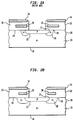
- FIGS. 3A and 3B a cross-sectional view of FIG. 1 is shown in which several semiconductor devices are formed on one substrate.
- FIG. 3A depicts the cross-section of DMOS devices of the prior art and
- FIG. 3B depicts the cross-section of DMOS devices incorporating the improvement of the present invention.
- the central device 12'' does not have junction extension region 28 because, as this device is surrounded by other devices, namely, 12' and 12''', it is less susceptible to surface breakdown.
- junction extension region 28 surrounds the outer portions of these outer devices, i.e. devices 12' and 12'''.
- the DMOS devices are constructed on an N+ substrate 42 containing an N- layer thereon which is preferably, although not necessarily, epitaxially grown.
- Major surface 24 is masked in an appropriate manner and a P- junction extension region 28, preferably in the shape of a ring if a round substrate is used, is implanted thereon.
- Major surface 24 is then masked in an appropriate manner and P regions 22, which make up the body of the DMOS devices, are implanted into major surface 24 and, after further masking, N+ regions 38, which form the source of the devices, are implanted on major surface 24 into P regions 22.
- An insulation layer 32 which is preferably SiO2, is grown on major surface 24 and gate and source terminals, corresponding to first field shield plate 30 and second field shield plate 34, respectively, are formed thereon.
- devices 12' and 12''' have a junction extension region 28 and two field shield plates 30, 34, configured in a manner described above in accordance with the present invention.
- first field shield plate 30 terminates above junction extension region 28 and second field shield plate 34 terminates after junction extension region 28 and preferably at edge 26.
- a DMOS device constructed in accordance with the present invention has an increased high voltage termination over the prior art and, experimentally I have found that the high voltage termination of a DMOS so constructed is approximately 30 volts higher than the high voltage termination of the prior art DMOS device of FIG. 3A.
- the DMOS device of the present invention and, for that matter, any semiconductor device having a surface P-N junction which is constructed in accordance with the present invention will have an increased high voltage termination and thus, such devices can be operated at higher voltages than their prior art counterparts without causing surface junction breakdown.
- the first field shield plate 30 which, as explained above, is preferably of polysilicon material, is masked, such as by utilizing photoresist techniques, in a manner such that the shield plate 30 terminates above junction extension region 28, i.e. essentially shortening shield plate 30.
- Shield plate 30 is preferably 0.5 ⁇ m thick and, for an N channel DMOS, is doped N+ type by using, for example, phosphorous as a dopant.
- Shield plate 30 may be formed by a chemical vapor deposition (CVD) method as known in the art.
- a thick insulation layer 33 comprising of SiO2 having a thickness of approximately 1.5 ⁇ m is deposited on first field shield plate 30 by a CVD method.
- a second field shield plate which comprises the metal source terminal 34 is disposed above the entire major surface 26, thereby sandwiching insulating layer 33 between it and first field shield plate 30.
- the second field shield plate 34 is preferably formed by an evaporation process as is known to those of ordinary skill in the art and its thickness is preferably between 1 - 1.5 ⁇ m.
- the P- junction extension region 28 terminates 5 ⁇ m beyond the edge of first field shield plate 30 and second field shield plate 34 terminates 15 ⁇ m beyond the edge of the P- junction termination region 28.
- the lateral distance between the respective edges of first field shield plate 30 and second field shield plate 34 is approximately 20 ⁇ m.
- the P- junction extension region 28 may be alternatively extended beyond the edge of field shield plate 30 as opposed to simply shortening plate 30.
Landscapes
- Electrodes Of Semiconductors (AREA)
- Bipolar Transistors (AREA)
- Element Separation (AREA)
Applications Claiming Priority (2)
| Application Number | Priority Date | Filing Date | Title |
|---|---|---|---|
| US163967 | 1993-12-08 | ||
| US08/163,967 US5959342A (en) | 1993-12-08 | 1993-12-08 | Semiconductor device having a high voltage termination improvement |
Publications (2)
| Publication Number | Publication Date |
|---|---|
| EP0657939A2 true EP0657939A2 (fr) | 1995-06-14 |
| EP0657939A3 EP0657939A3 (fr) | 1995-09-13 |
Family
ID=22592405
Family Applications (1)
| Application Number | Title | Priority Date | Filing Date |
|---|---|---|---|
| EP94308845A Withdrawn EP0657939A3 (fr) | 1993-12-08 | 1994-11-30 | Dispositif semi-conducteur avec une terminaison à haute tension améliorée et son procédé de fabrication. |
Country Status (3)
| Country | Link |
|---|---|
| US (1) | US5959342A (fr) |
| EP (1) | EP0657939A3 (fr) |
| JP (1) | JPH07202203A (fr) |
Cited By (3)
| Publication number | Priority date | Publication date | Assignee | Title |
|---|---|---|---|---|
| US9179773B2 (en) | 2008-06-27 | 2015-11-10 | Ssw Holding Company, Inc. | Spill containing refrigerator shelf assembly |
| US10317129B2 (en) | 2011-10-28 | 2019-06-11 | Schott Ag | Refrigerator shelf with overflow protection system including hydrophobic layer |
| US11786036B2 (en) | 2008-06-27 | 2023-10-17 | Ssw Advanced Technologies, Llc | Spill containing refrigerator shelf assembly |
Families Citing this family (4)
| Publication number | Priority date | Publication date | Assignee | Title |
|---|---|---|---|---|
| US6194750B1 (en) * | 1999-02-01 | 2001-02-27 | Lucent Technologies, Inc. | Integrated circuit comprising means for high frequency signal transmission |
| US6211541B1 (en) | 1999-02-01 | 2001-04-03 | Lucent Technologies, Inc. | Article for de-embedding parasitics in integrated circuits |
| US8106487B2 (en) | 2008-12-23 | 2012-01-31 | Pratt & Whitney Rocketdyne, Inc. | Semiconductor device having an inorganic coating layer applied over a junction termination extension |
| ES2613885T3 (es) | 2009-11-04 | 2017-05-26 | Ssw Holding Company, Inc. | Superficies de aparatos de cocción que tienen un patrón de confinamiento de salpicaduras y procedimientos de fabricación de las mismas |
Family Cites Families (14)
| Publication number | Priority date | Publication date | Assignee | Title |
|---|---|---|---|---|
| US5187552A (en) * | 1979-03-28 | 1993-02-16 | Hendrickson Thomas E | Shielded field-effect transistor devices |
| DE3046749C2 (de) * | 1979-12-10 | 1986-01-16 | Sharp K.K., Osaka | MOS-Transistor für hohe Betriebsspannungen |
| US4947232A (en) * | 1980-03-22 | 1990-08-07 | Sharp Kabushiki Kaisha | High voltage MOS transistor |
| JPS5817676A (ja) * | 1981-07-24 | 1983-02-01 | Toshiba Corp | 高耐圧プレ−ナ型半導体装置 |
| US4561170A (en) * | 1984-07-02 | 1985-12-31 | Texas Instruments Incorporated | Method of making field-plate isolated CMOS devices |
| JP2585331B2 (ja) * | 1986-12-26 | 1997-02-26 | 株式会社東芝 | 高耐圧プレーナ素子 |
| IT1217214B (it) * | 1988-04-27 | 1990-03-14 | Sgs Thomson Microelectronics | Circuito integrato per alta tensione con isolamento a giunzione |
| US5237193A (en) * | 1988-06-24 | 1993-08-17 | Siliconix Incorporated | Lightly doped drain MOSFET with reduced on-resistance |
| JPH0666329B2 (ja) * | 1988-06-30 | 1994-08-24 | 株式会社東芝 | 半導体装置の製造方法 |
| EP0360036B1 (fr) * | 1988-09-20 | 1994-06-01 | Siemens Aktiengesellschaft | Jonction pn plane à tenue en tension élévée |
| US5208471A (en) * | 1989-06-12 | 1993-05-04 | Hitachi, Ltd. | Semiconductor device and manufacturing method therefor |
| US5204545A (en) * | 1989-11-22 | 1993-04-20 | Mitsubishi Denki Kabushiki Kaisha | Structure for preventing field concentration in semiconductor device and method of forming the same |
| JPH03171774A (ja) * | 1989-11-30 | 1991-07-25 | Toshiba Corp | 高耐圧プレーナ素子 |
| JP2904545B2 (ja) * | 1990-05-08 | 1999-06-14 | 株式会社東芝 | 高耐圧プレーナ型半導体素子およびその製造方法 |
-
1993
- 1993-12-08 US US08/163,967 patent/US5959342A/en not_active Expired - Lifetime
-
1994
- 1994-11-30 EP EP94308845A patent/EP0657939A3/fr not_active Withdrawn
- 1994-12-02 JP JP6323938A patent/JPH07202203A/ja active Pending
Cited By (9)
| Publication number | Priority date | Publication date | Assignee | Title |
|---|---|---|---|---|
| US9179773B2 (en) | 2008-06-27 | 2015-11-10 | Ssw Holding Company, Inc. | Spill containing refrigerator shelf assembly |
| US9207012B2 (en) | 2008-06-27 | 2015-12-08 | Ssw Holding Company, Inc. | Spill containing refrigerator shelf assembly |
| US9532649B2 (en) | 2008-06-27 | 2017-01-03 | Ssw Holding Company, Inc. | Spill containing refrigerator shelf assembly |
| US10130176B2 (en) | 2008-06-27 | 2018-11-20 | Ssw Holding Company, Llc | Spill containing refrigerator shelf assembly |
| US10827837B2 (en) | 2008-06-27 | 2020-11-10 | Ssw Holding Company, Llc | Spill containing refrigerator shelf assembly |
| US11191358B2 (en) | 2008-06-27 | 2021-12-07 | Ssw Advanced Technologies, Llc | Spill containing refrigerator shelf assembly |
| US11786036B2 (en) | 2008-06-27 | 2023-10-17 | Ssw Advanced Technologies, Llc | Spill containing refrigerator shelf assembly |
| US12096854B2 (en) | 2008-06-27 | 2024-09-24 | Ssw Advanced Technologies, Llc | Spill containing refrigerator shelf assembly |
| US10317129B2 (en) | 2011-10-28 | 2019-06-11 | Schott Ag | Refrigerator shelf with overflow protection system including hydrophobic layer |
Also Published As
| Publication number | Publication date |
|---|---|
| EP0657939A3 (fr) | 1995-09-13 |
| JPH07202203A (ja) | 1995-08-04 |
| US5959342A (en) | 1999-09-28 |
Similar Documents
| Publication | Publication Date | Title |
|---|---|---|
| US11916066B2 (en) | MOSFET device of silicon carbide having an integrated diode and manufacturing process thereof | |
| KR100256903B1 (ko) | 전계효과 트랜지스터 | |
| US5861657A (en) | Graded concentration epitaxial substrate for semiconductor device having resurf diffusion | |
| US5404040A (en) | Structure and fabrication of power MOSFETs, including termination structures | |
| EP0537684B1 (fr) | Transistor MOS double-diffusé latéral et sa méthode de fabrication | |
| US6468837B1 (en) | Reduced surface field device having an extended field plate and method for forming the same | |
| US4769685A (en) | Recessed-gate junction-MOS field effect transistor | |
| US6110804A (en) | Method of fabricating a semiconductor device having a floating field conductor | |
| US5486718A (en) | High voltage planar edge termination structure and method of making same | |
| EP0851505A2 (fr) | Dispositif semi-conducteur comprenant une structure de terminaison à haute tension à région de façonnage de champ enterrée | |
| CA3191367C (fr) | Conception et fabrication de dispositifs d'alimentation ameliores | |
| JP2000156503A (ja) | Mosゲートデバイスおよびその製造プロセス | |
| EP0382165B1 (fr) | Dispositif semi-conducteur à haute tension ayant une structure de type silicium sur isolant avec une résistance à l'état conducteur réduite | |
| WO2003003452A2 (fr) | Composant semi-conducteur et son procede de fabrication | |
| EP0660416A1 (fr) | Dispositif semi-conducteur avec surface de bord réduite et haute tension de claquage | |
| US5959342A (en) | Semiconductor device having a high voltage termination improvement | |
| US5321291A (en) | Power MOSFET transistor | |
| US5047820A (en) | Semi self-aligned high voltage P channel FET | |
| US4125415A (en) | Method of making high voltage semiconductor structure | |
| US20230352577A1 (en) | Vertical shielded gate accumulation field effect transistor | |
| US20250374622A1 (en) | Semiconductor switching device | |
| CA3191347C (fr) | Conception et fabrication de dispositifs d'alimentation ameliores | |
| CN119170640A (zh) | 半导体器件及其制备方法 | |
| HK1014803A (en) | Structure and fabrication of power mosfets, including termination structure | |
| KR20000010289A (ko) | 전력용 반도체소자 및 그 제조방법 |
Legal Events
| Date | Code | Title | Description |
|---|---|---|---|
| PUAI | Public reference made under article 153(3) epc to a published international application that has entered the european phase |
Free format text: ORIGINAL CODE: 0009012 |
|
| AK | Designated contracting states |
Kind code of ref document: A2 Designated state(s): DE FR GB |
|
| PUAL | Search report despatched |
Free format text: ORIGINAL CODE: 0009013 |
|
| AK | Designated contracting states |
Kind code of ref document: A3 Designated state(s): DE FR GB |
|
| 17P | Request for examination filed |
Effective date: 19960229 |
|
| 17Q | First examination report despatched |
Effective date: 19961218 |
|
| STAA | Information on the status of an ep patent application or granted ep patent |
Free format text: STATUS: THE APPLICATION HAS BEEN WITHDRAWN |
|
| 18W | Application withdrawn |
Withdrawal date: 19970927 |