EP0658902B1 - Mémoire à semi-conducteurs avec un circuit d'écriture/lecture de données à haute vitesse et basse puissance - Google Patents
Mémoire à semi-conducteurs avec un circuit d'écriture/lecture de données à haute vitesse et basse puissance Download PDFInfo
- Publication number
- EP0658902B1 EP0658902B1 EP94119890A EP94119890A EP0658902B1 EP 0658902 B1 EP0658902 B1 EP 0658902B1 EP 94119890 A EP94119890 A EP 94119890A EP 94119890 A EP94119890 A EP 94119890A EP 0658902 B1 EP0658902 B1 EP 0658902B1
- Authority
- EP
- European Patent Office
- Prior art keywords
- write
- read
- control signal
- data
- buses
- Prior art date
- Legal status (The legal status is an assumption and is not a legal conclusion. Google has not performed a legal analysis and makes no representation as to the accuracy of the status listed.)
- Expired - Lifetime
Links
- 239000004065 semiconductor Substances 0.000 title claims description 13
- 230000004044 response Effects 0.000 claims description 15
- 230000015654 memory Effects 0.000 claims description 10
- 101100286980 Daucus carota INV2 gene Proteins 0.000 claims description 6
- 101100397045 Xenopus laevis invs-b gene Proteins 0.000 claims description 6
- 101100508840 Daucus carota INV3 gene Proteins 0.000 claims description 4
- 101150110971 CIN7 gene Proteins 0.000 claims description 3
- 101150110298 INV1 gene Proteins 0.000 claims description 3
- 101100397044 Xenopus laevis invs-a gene Proteins 0.000 claims description 3
- 238000009877 rendering Methods 0.000 claims 5
- 101150070189 CIN3 gene Proteins 0.000 claims 3
- -1 INV5 Proteins 0.000 claims 3
- 108020001305 NR1 subfamily Proteins 0.000 claims 1
- 108020002076 NR2 subfamily Proteins 0.000 claims 1
- 238000010586 diagram Methods 0.000 description 9
- 230000004913 activation Effects 0.000 description 6
- 230000001360 synchronised effect Effects 0.000 description 6
- 230000000295 complement effect Effects 0.000 description 5
- 230000002093 peripheral effect Effects 0.000 description 2
- 239000000470 constituent Substances 0.000 description 1
- 238000010276 construction Methods 0.000 description 1
- 230000001419 dependent effect Effects 0.000 description 1
- 238000000034 method Methods 0.000 description 1
- 230000002035 prolonged effect Effects 0.000 description 1
- 230000000630 rising effect Effects 0.000 description 1
Images


Classifications
-
- G—PHYSICS
- G11—INFORMATION STORAGE
- G11C—STATIC STORES
- G11C11/00—Digital stores characterised by the use of particular electric or magnetic storage elements; Storage elements therefor
- G11C11/21—Digital stores characterised by the use of particular electric or magnetic storage elements; Storage elements therefor using electric elements
- G11C11/34—Digital stores characterised by the use of particular electric or magnetic storage elements; Storage elements therefor using electric elements using semiconductor devices
- G11C11/40—Digital stores characterised by the use of particular electric or magnetic storage elements; Storage elements therefor using electric elements using semiconductor devices using transistors
- G11C11/401—Digital stores characterised by the use of particular electric or magnetic storage elements; Storage elements therefor using electric elements using semiconductor devices using transistors forming cells needing refreshing or charge regeneration, i.e. dynamic cells
- G11C11/4063—Auxiliary circuits, e.g. for addressing, decoding, driving, writing, sensing or timing
- G11C11/407—Auxiliary circuits, e.g. for addressing, decoding, driving, writing, sensing or timing for memory cells of the field-effect type
- G11C11/409—Read-write [R-W] circuits
- G11C11/4096—Input/output [I/O] data management or control circuits, e.g. reading or writing circuits, I/O drivers or bit-line switches
-
- G—PHYSICS
- G11—INFORMATION STORAGE
- G11C—STATIC STORES
- G11C11/00—Digital stores characterised by the use of particular electric or magnetic storage elements; Storage elements therefor
- G11C11/21—Digital stores characterised by the use of particular electric or magnetic storage elements; Storage elements therefor using electric elements
- G11C11/34—Digital stores characterised by the use of particular electric or magnetic storage elements; Storage elements therefor using electric elements using semiconductor devices
- G11C11/40—Digital stores characterised by the use of particular electric or magnetic storage elements; Storage elements therefor using electric elements using semiconductor devices using transistors
-
- G—PHYSICS
- G11—INFORMATION STORAGE
- G11C—STATIC STORES
- G11C7/00—Arrangements for writing information into, or reading information out from, a digital store
- G11C7/10—Input/output [I/O] data interface arrangements, e.g. I/O data control circuits, I/O data buffers
- G11C7/1048—Data bus control circuits, e.g. precharging, presetting, equalising
Definitions
- the present invention relates to a semiconductor memory device and, more particularly, to an improvement in a data read/write circuit in a so-called synchronous dynamic random access memory (synchronous DRAM).
- synchronous DRAM synchronous dynamic random access memory
- a synchronous DRAM This DRAM operates in synchronism with an external clock and employs a pipeline structure to perform a high speed data read/write operation.
- Such a synchronous DRAM is constituted as shown in FIG. 5. Note that only a data read/write circuit portion is shown and a memory cell array as well as peripheral circuits for selecting memory cell(s) are omitted in Fig. 5.
- a command control circuit 10 receives external input signals RAS , CAS and WE as well as an external clock signal CLK and produces a write activation signal WR and a read activation signal RE.
- An internal clock generation circuit 20 receives the external clock signal CLK and generates internal clock signals ICLK1, ICLK2 and ICLK3.
- a write/read control circuit 30 receives the write activation signal WR, the read activation signal RE and the internal clock signal ICLK2 and outputs a writing pulse signal WPAL1 and a reading pulse signal RPAL.
- a write data buffer 40 comprises a D-F/F circuit which receives an external input data from a data terminal DQ and the internal clock signal ICLK1 and outputs a write data WDATA1.
- a write data latching circuit 50 also comprises a D-F/F circuit which latches the write data WDATA1 in synchronism with the internal clock signal ICLK2 and outputs it as a write data WDATA2.
- a read/write bus driving circuit 62 receives the write data WDATA2 and the writing pulse signal WPAL1 and drives true and complementary read/write buses RWBUST and RWBUSN.
- a write switching circuit 70 receives data from the read/write buses RWBUST and RWBUSN and drives true and complementary write buses WBUST and WBUSN while outputting a write switching signal WSW. When either of data sent from the read/write buses RWBUST and RWBUSN is at the low level (hereafter referred to as L), the write switching circuit 70 sets the write switching signal WSW to a high level (hereafter referred to as H) and outputs write-data onto the write buses WBUST and WBUSN.
- L low level
- H high level
- the write switching circuit 70 sets the write switching signal WSW to L. That is, the outputs of the read/write bus driving circuit 62 serve as both reading data and control information.
- a sense amplifier 80 receives data from the write buses WBUST and WBUSN when the write switching signal WSW is H, whereas outputs read-data to true and complementary read buses RBUST and RBUSN when the write switching signal WSW is L.
- a first data amplifier circuit 90 receives the data from the read buses RBUST and RBUSN and a reading pulse signal RPAL and outputs data to the read/write buses RWBUST and RWBUSN. Note that either voltage indicating H or the voltage indicating L transferred in to the buses RWBUST and RWBUSN by the data amplifier 90 is regarded as H by the write switching circuit 70.
- a second data amplifier circuit 100 receives data from the read/write buses RWBUST and RWBUSN and the reading pulse signal RPAL and outputs read data RDATA1.
- a read data latching circuit 110 comprises a D-F/F circuit which receives the read data RDATA1 and the internal clock signal ICLK3 and outputs a read data RDATA2.
- a data out buffer 120 receives the read data RDATA2 and outputs an output data to the terminal DQ.
- the operation of the synchronous DRAM as shown in FIG. 5 is described below by referring to FIG. 6.
- An active command is first inputted to select one word line (not shown) and the input signals RAS, CAS and WE are then set to H, L, and L, respectively, at a cycle C1 in synchronism with the leading edge of the external clock signal CLK.
- the command control circuit 10 thereby outputs the write active high signal WR during the cycle C1.
- the clock generator 20 generates the internal clock signals ICLK1, ICLK2 and ICLK3 in the form of one-shot pulse in cycles C1, C2 and C3, respectively. Note that the write active high signal WR is changed to the L in the cycle C2.
- the writing pulse signal WPAL1 becomes H during the cycle C2.
- Write-data supplied to the terminal DQ is valid at the leading edge of the external input clock CLK in the cycle C1, so that the write data buffer circuit 40 latches the write-data in synchronism with the one-shot internal clock signal ICLK1 at the cycle C1 and outputs the write data WDATA1.
- the write data latching circuit 50 latches the write data WDATA1 in synchronism with the one-shot internal clock signal ICLK2 and outputs the write data WDATA2. In response further to the one-shot internal clock signal ICLK2, the write/read control circuit 30 brings the writing pulse signal WPAL1 into H during the cycle C2.
- the read/write bus driving circuit 62 fetches the write data WDATA2 and drives the read/write buses RWBUST and RWBUSN in response thereto. Since either one of the potentials on the read/write buses RWBUST and RWBUSN takes the L, the write switching signal WSW becomes H and the write-data is transferred to the sense amplifier 80 through the write switching circuit 70 and the write buses WBUST and WBUSN. The write-data is thus stored in the selected memory cell (not shown).
- the command control circuit 10 detects the input signals RAS, CAS and WE which are set to H, L and H, respectively, at the leading edge of the external clock signal CLK in the cycle C2 and brings the read activation signal RE into H during the cycle C2.
- the read activation signal RE is changed to L in the cycle C3.
- the internal clock signals ICLK1, ICLK2, and ICLK3 are generated in the form of one-shot pulse at the cycles C2, C3 and C4, respectively.
- the one-shot internal clock signal ICLK2 in the cycle C3 causes the reading pulse signal RPAL to become one-shot H.
- the first data amplifier circuit 90 receives a read-data responsive to the data stored in the selected memory cell from the sense amplifier 80 through the read buses RBUST and RBUSN and drives the read/write buses RWBUST and RWBUSN in response thereto.
- the read-data on the read/write buses RWBUST and RWBUSN are then amplified by the second data amplifier circuit 100 and are outputted as the read-data RDATA1.
- the read data latching circuit 110 latches the read-data RDATA1 and outputs the read-data RDATA2.
- the outputted read-data RDATA2 is then outputted to the terminal DQ through the data out buffer circuit 120.
- FIG. 7 there are shown detailed circuits of the read/write bus driving circuit 62, the write switching circuit 70 and the first data amplifier circuit 90.
- the read/write bus driving circuit 62 comprises an inverter INV1 receiving the write data WDATA2, an inverter INV2 receiving the writing pulse signal WPAL1, two NOR gates NR1 and NR2 receiving the write data WDATA2 and the output of the inverter INV2, two NOR gates NR3 and NR4 receiving the output of the inverter INV1 and the output of the inverter INV2, a P-channel MOS transistor Tr1 receiving at the gate thereof the output of the NOR gate NR1 and connected between the power source and the true read/write bus RWBUST, an N-channel MOS transistor Tr2 receiving at the gate thereof the output of the NOR gate NR2 and connected between the ground and the read/write bus RWBUST, a P-channel MOS transistor Tr3 receiving at its gate the output of the NOR gate NR3 and connected between the power source and the complementary read/write bus RWBUSN, and an N-channel MOS transistor Tr4 receiving the output of the NOR gate NR4 and connected between the ground and the
- the write switching circuit 70 comprises a NAND gate ND2 performing a NAND operation on the data of the read/write buses RWBUST and RWBUSN and producing the write switching signal WSW, a transfer gate TG1 receiving the write switching signal WSW and inserted between the read/write bus RWBUST and the write bus WBUST, a transfer gate TG2 receiving the write switching signal WSW and inserted between the read/write bus RWBUSN and the write bus WBUSN, a P-channel MOS transistor Tr11 receiving the write switching signal WSW and is arranged between the power source and the write bus WBUST, and a P-channel MOS transistor Tr12 receiving the write switching signal WSW and is arranged between the power source and the write bus WBUSN.
- the first data amplifier circuit 90 is controlled by the reading pulse signal RPAL to amplify the voltage difference between the read buses RBUST and RBUSN. That is, the circuit 90 comprises a differential amplifier 91 connected between the read buses RBUST and RBUSN, N-channel MOS transistors Tr8 and Tr10 which are connected in series between the ground and the read/write bus RWBUST and N-channel MOS transistors Tr7 and Tr9 which are arranged between the ground and the read/write bus RWBUSN in series.
- either one of the read/write buses RWBUST and RWBUSN becomes H and the other bus becomes L in accordance with the level of the write-data WDATA2.
- the write switching signal WSW thereby becomes H and the transfer gates TG1 and TG2 are turned on.
- the data in the read/write buses RWBUST and RWBUSN are transferred to the write buses WBUST and WBUSN which has been precharged to H beforehand by the transistors Tr11 and Tr12.
- both the read/write bus RWBUST and the write bus WBUST become H and both the read/write bus RWBUSN and the write bus WBUSN become L.
- both the read/write buses RWBUST and RWBUSN are precharged to H.
- the write switching signal WSW becomes L and the transfer gates TG1 and TG2 are turned off.
- the write buses WBUST and WBUSN are thus precharged to H by the transistors Tr11 and Tr12.
- the reading pulse signal RPAL is L during the cycle C2
- the transistors Tr9 and Tr10 are turned off, and the differential amplifier 91 is not activated, the read buses RBUST and RBUSN being thereby balanced at a precharge level.
- the reading pulse signal RPAL becomes H to activate the differential amplifier 91, so that a potential difference is produced between the read buses RBUSN and RBUST in accordance with the data from the sense amplifier 80 in response to the data stored in the selected memory cell.
- the transistors Tr9 and Tr10 are turned on.
- the transistors Tr1 and Tr3 in the read/write bus driving circuit 62 are turned on and the N-type transistors Tr2 and Tr4 are turned off. Therefore, a first DC path passing through the transistor Tr1, the read/write bus RWBUST and the transistors Tr7 and Tr9 and a second DC path passing through the transistor Tr3, the read/write bus RBUSN, and the transistors Tr8 and Tr10 exist between the power source and the ground.
- the levels of the read/write buses RWBUST and RWBUSN are thereby determined by the ratio of on-resistances of those transistors in the first and second DC paths.
- the potential difference thus appearing between the read/write buses RWBUSN and RWBUST is further amplified by the second data amplifier circuit 100 to obtain the read-data RDATA1.
- the reading pulse signal RPAL becomes L
- the read buses RBUST and RBUSN are balanced at and precharged to the initial level and the read/write buses RWBUST and RWBUSN are precharged to the power source level.
- the reading pulse is generated at a high speed by transferring data from the sense amplifier to the second data amplifier 100 at a very-small potential difference.
- the transistors Tr1 and Tr3 are used not only to determine the levels of the read/write buses RWBUST and RWBUSN during the read operation and but also to precharge them during the write operation.
- the driving capacity of the transistors Tr1 and Tr3 is required to be made small as mentioned above. For this reason, during the write operation, it takes a long period of time to precharge either one of the read/write buses RWBUS which has falled down to the ground level up to the power source level, so that the data write cycle is prolonged.
- the capacity of the precharging transistors Tr1 and Tr3 would be increased in order to shorten the cycle time, the current consumed in the DC path would increase.
- a semiconductor memory comprising a pair of read/write buses, a first bus driving circuit responding to a write-data and driving one of the read/write buses to a first potential and the other of the read/write buses to a second potential during a write operation, a second bus driving circuit responding to a read-data and driving one of the read/write buses to a third potential and the other of them to a fourth potential during a read operation, and a third bus driving circuit cooperates with the first bus driving circuit to precharge both of the read/write buses to a precharge level for a predetermined time period after the write operation is completed.
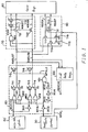
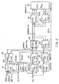
- FIG. 1 there is shown a circuit diagram of a synchronous DRAM according to the first embodiment of the present invention, in which the same constituents as those shown in FIG. 7 are denoted by the same reference numerals and symbols to omit the further description thereof. Also in FIG. 1, only the data read/write circuit is shown and a memory cell array and peripheral circuits for selecting one or more memory cells in the cell array are omitted since they are not directly related to the present invention and are well known in the art.
- the memory device includes a read/write bus driving circuit 60 different from the read/write bus driving circuit 62 shown in FIG. 7.
- this circuit 60 further includes, in addition to the circuit components shown in FIG. 7, a delay circuit 601 composed of inverters INV3 to INV5 and receiving the output of an inverter INV2, a NAND gate ND1 for receiving the outputs of the inverter INV2, and the delay circuit 601, a P-channel MOS transistor Tr5 receiving a writing pulse signal WPAL2 produced by the NAND gate ND1 and arranged between the power source line and the true read/write bus RWBUST, and a P-channel MOS transistor Tr6 receiving the writing pulse signal WPAL2 and is arranged between the power source line and the complementary read/write bus RWBUSN.
- a delay circuit 601 composed of inverters INV3 to INV5 and receiving the output of an inverter INV2, a NAND gate ND1 for receiving the outputs of the inverter INV2, and the delay circuit 601, a P-channel MOS transistor Tr5 receiving a writing pulse signal WPAL2 produced by the NAND gate ND1 and arranged between the
- the delay circuit 601 and the NAND gate ND1 constitute a one-shot pulse generator responsive to the writing pulse signal WPAL1
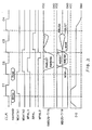
- the writing pulse signal WPAL2 is generated in the form of a one-shot pulse in response to the falling edge of the signal WPAL1, as shown in FIG. 2.
- the transistors Tr5 and Tr6 are thereby turned on. That is, by the writing pulse signal WPAL1 changing to L, i.e., by the completion of the data writing, the transistors Tr1 and Tr3 are turned on and the transistors Tr5 and Tr6 are also turned on to precharge the read/write buses RWBUST and RWBUSN up to the power source level.
- the writing pulse signal WPAL2 is a one-shot pulse and thus returned to H at time when the read operation is performed.
- the transistors Tr5 and Tr6 are thereby turned off during the read operation and only the transistors Tr1 and Tr3 form a conductive path berween the power supply line and the read/write buses RWBUST and RWBUSN.
- a d.c. current flows through the transistors Tr1, Tr7 and Tr9 (Tr3, Tr8 and Tr10); however, since each of the transistors Tr1 and Tr3 is formed with a relatively small current capability, so that the power consumption is suppressed.
- the potentials on both the buses RWBUST and RWBUSN during the read operation are designed to be higher then the threshold voltage of the NAND gate ND2 in the writing switching circuit 70, the switching signal WSW is maintained at the low level.
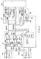
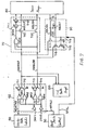
- a read/write bus driving circuit 61 employs a NOR gate NR5 and an inverter INV6 in place of the delay circuit 601 and the NAND gate ND1 as shown in FIG. 1.
- the NOR gate NR5 receives the writing pulse signal WPAL1 and the reading pulse signal RPAL and the inverter INV6 receives the output of the NOR gate NR5.
- the output of the inverter INV6 is used as a writing pulse signal WPAL3 which is in turn supplied to the transistors Tr5 and Tr6.
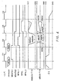
- the writing pulse signal WPAL1 becomes L in the cycle C2
- the writing pulse signal WPAL3 becomes L and the transistors Tr5 and Tr6 are turned on because the reading pulse signal RPAL is also L. That is, the transistors Tr1 and Tr3 are turned on immediately after the wriging pulse signal WPAL1 has been turned on and the write operation has completed, and the transistors Tr5 and Tr6 are also turned on at the time of precharging the read/write buses RWBUST and RWBUSN to the power source level to precharge the read/write buses RWBUST and RWBUSN to the power source level.
- the reading pulse signal RPAL becomes H at the time of performing the read operation in the cycle C3
- the writing pulse signal WRPAL3 returns to H. Therefore, the transistors Tr5 and Tr6 are turned off during the read operation and only the transistors Tr1 and Tr3 become the transistors for supplying power to the read/write buses RWBUST and RWBUSN.
- the first read/write bus driving circuit charges both read/write bus pair to the first potential in a period other than the write operation and a third read/write bus driving circuit further energizes the charging. That is, it is possible to sufficiently or quickly charge the read/write buses and moreover shorten the cycle time without increasing the size of driving element in the first read/write bus driving circuit related to the read operation and increasing the power consumption for the read operation by driving the both read/write bus pair to the first potential in at least a part of the period until the next write or read operation is started after the write operation has completed.
Landscapes
- Engineering & Computer Science (AREA)
- Microelectronics & Electronic Packaging (AREA)
- Computer Hardware Design (AREA)
- Databases & Information Systems (AREA)
- Dram (AREA)
- Static Random-Access Memory (AREA)
Claims (8)
- Mémoire à semi-conducteurs comprenant une paire de bus de lecture/écriture (RWBUS T/N) par l'intermédiaire desguels des signaux de données d'écriture sont transférés dans une opération d'écriture et des signaux de données de lecture sont transférés dans une opération de lecture, un premier circuit d'attaque de bus (60) répondant à des données d'écriture (WDATA2) et amenant un desdits bus de lecture/écriture à un premier potentiel (H) et l'autre desdits bus de lecture/écriture à un deuxième potentiel durant ladite opération d'écriture (L), ledit premier circuit d'attaque de bus ayant un circuit de précharge (Tr1, Tr3) réalisant un chemin de conduction entre une ligne de tension d'alimentation (VCC) et lesdits bus de lecture/écriture, pour précharger lesdits deux bus de lecture/écriture jusqu'à un niveau de précharge (H) en réponse à l'achèvement de ladite opération d'écriture, et ledit premier circuit d'attaque de bus réalisant ledit chemin de conduction durant ladite opération de lecture ; un deuxième circuit d'attaque de bus (90) répondant à des données de lecture et amenant un desdits bus de lecture/écriture à un troisième potentiel et l'autre desdits bus de lecture/écriture à un quatrième potentiel durant l'opération de lecture, et un troisième circuit d'attaque de bus (Tr5, Tr6) coopérant avec ledit circuit de précharge pour précharger lesdits deux bus de lecture/écriture jusqu'audit niveau de précharge pendant une période prédéterminée en réponse à l'achèvement de ladite opération d'écriture.
- Mémoire à semi-conducteurs selon la revendication 1, dans laquelle ledit premier circuit d'attaque de bus est activé par un signal de commande d'écriture (WPAL1) et dans lequel ledit troisième circuit d'attaque de bus est activé lorsque ledit signal de commande d'écriture disparaít.
- Mémoire à semi-conducteurs selon la revendication 1, dans laquelle ledit premier circuit d'attaque de bus est activé par un signal de commande d'écriture (WPAL1) et dans laquelle ledit deuxième circuit d'attaque de bus est activé par un signal de commande de lecture (RPAL), ledit troisième circuit d'attaque de bus étant activé durant une période où aucun des deux signaux parmi ledit signal de commande d'écriture et ledit signal de commande de lecture n'existe.
- Mémoire à semi-conducteurs selon la revendication 2, dans laquelle ledit troisième circuit d'attaque de bus comprend un générateur d'impulsion monostable INV3, INV4, INV5, ND1 ; NR5, INV6 répondant à la disparition dudit signal de commande d'écriture et produisant un signal d'impulsion monostable (WPAL2 ; WPAL3), et des transistors de précharge (Tr5, Tr6) préchargeant lesdits bus de lecture/écriture en réponse audit signal d'impulsion monostable.
- Mémoire à semi-conducteurs selon la revendication 3, dans laquelle ledit troisième circuit d'attaque de bus comprend un circuit de grille (NR5) répondant à un fait selon lequel aucun des deux signaux parmi ledit signal de commande d'écriture et ledit signal de commande de lecture n'existe et produisant un signal de validation de précharge (WPAL3), et des transistors de précharge (Tr5, Tr6) préchargeant lesdits bus de lecture/écriture en réponse audit signal de validation de précharge.
- Mémoire à semi-conducteurs comprenant un bus de données (RWBUS T), un premier transistor (Tr1) connecté entre ledit bus de données et une première ligne d'alimentation (VCC), un deuxième transistor (Tr2) connecté entre ledit bus de données et une deuxième ligne d'alimentation (GND), un circuit de grille (INV1, INV2, NR1, NR2) recevant des données d'écriture (WDATA2) et un signal de commande d'écriture (WPAL1) et rendant un desdits premier et deuxième transistors conducteur en réponse auxdites données d'écriture durant le moment où ledit signal de commande d'écriture est à un niveau actif (H), ledit circuit de grille rendant en outre lesdits premier et deuxième transistors respectivement conducteur et non-conducteur, durant le moment où ledit signal de commande d'écriture est à un niveau inactif (L), des troisième et quatrième transistors (Tr7 et Tr9) étant connectés en série entre ledit bus de données et ladite deuxième ligne d'alimentation, des premiers moyens (80) pour délivrer des données de lecture audit troisième transistor, des deuxièmes moyens (30) pour rendre ledit quatrième transistor conducteur durant le moment où un signal de commande de lecture (RPAL) est à un niveau actif (H) et non-conducteur durant le moment où ledit signal de commande de lecture est à un niveau inactif (L), ledit circuit de grille rendant en outre lesdits premier et deuxième transistors respectivement conducteur et non-conducteur, durant le moment où ledit signal de commande de lecture est audit niveau actif, un cinquième transistor (Tr5) connecté entre ledit bus de données et ladite première ligne d'alimentation, et des troisièmes moyens INV3, INV4, INV5, ND1 ; NR5, INV6 sensibles au moins audit signal de commande d'écriture pour rendre ledit cinquième transistor conducteur pendant une période prédéterminée en réponse à un passage dudit signal de commande d'écriture dudit niveau actif audit niveau inactif.
- Mémoire selon la revendication 6, dans laquelle lesdits troisièmes moyens comprennent un générateur d'impulsion monostable INV3, INV4, INV5, ND1 ; NR5, INV6 produisant une impulsion monostable (WPAL2 : WPAL3) en réponse audit passage dudit signal de commande d'écriture dudit niveau actif audit niveau inactif, et dans laquelle ledit cinquième transistor est rendu conducteur en réponse à ladite impulsion monostable.
- Mémoire selon la revendication 6, dans laquelle lesdits troisièmes moyens répondent en outre audit signal de commande de lecture et produisent un signal de commande de précharge (WPAL3) durant le moment où à la fois ledit signal de commande d'écriture et ledit signal de commande de lecture sont audit niveau inactif, ledit cinquième transistor étant rendu conducteur en réponse audit signal de commande de précharge.
Applications Claiming Priority (3)
| Application Number | Priority Date | Filing Date | Title |
|---|---|---|---|
| JP5314638A JP2906957B2 (ja) | 1993-12-15 | 1993-12-15 | 半導体メモリ装置 |
| JP314638/93 | 1993-12-15 | ||
| JP31463893 | 1993-12-15 |
Publications (3)
| Publication Number | Publication Date |
|---|---|
| EP0658902A2 EP0658902A2 (fr) | 1995-06-21 |
| EP0658902A3 EP0658902A3 (fr) | 1996-12-18 |
| EP0658902B1 true EP0658902B1 (fr) | 2000-03-08 |
Family
ID=18055735
Family Applications (1)
| Application Number | Title | Priority Date | Filing Date |
|---|---|---|---|
| EP94119890A Expired - Lifetime EP0658902B1 (fr) | 1993-12-15 | 1994-12-15 | Mémoire à semi-conducteurs avec un circuit d'écriture/lecture de données à haute vitesse et basse puissance |
Country Status (5)
| Country | Link |
|---|---|
| US (1) | US5502684A (fr) |
| EP (1) | EP0658902B1 (fr) |
| JP (1) | JP2906957B2 (fr) |
| KR (1) | KR0146863B1 (fr) |
| DE (1) | DE69423307T2 (fr) |
Families Citing this family (11)
| Publication number | Priority date | Publication date | Assignee | Title |
|---|---|---|---|---|
| US5546338A (en) * | 1994-08-26 | 1996-08-13 | Townsend And Townsend Khourie And Crew | Fast voltage equilibration of differential data lines |
| JP3277112B2 (ja) * | 1996-01-31 | 2002-04-22 | 株式会社東芝 | 半導体記憶装置 |
| KR19980052743A (ko) * | 1996-12-24 | 1998-09-25 | 김광호 | 수평편향 회로의 직선성 코일 |
| JPH113588A (ja) * | 1997-06-12 | 1999-01-06 | Nec Corp | 半導体記憶装置 |
| DE19828657C2 (de) * | 1998-06-26 | 2001-01-04 | Siemens Ag | Integrierter Speicher |
| JP2000231791A (ja) * | 1998-12-10 | 2000-08-22 | Fujitsu Ltd | 半導体記憶装置及びデータバスのリセット方法 |
| JP3784979B2 (ja) * | 1999-02-09 | 2006-06-14 | 株式会社東芝 | バス駆動回路 |
| KR100334574B1 (ko) * | 2000-01-31 | 2002-05-03 | 윤종용 | 풀-페이지 모드를 갖는 버스트-타입의 반도체 메모리 장치 |
| TWI423256B (zh) * | 2008-10-29 | 2014-01-11 | Etron Technology Inc | 資料感測裝置與方法 |
| CN111627474B (zh) * | 2020-05-29 | 2022-06-10 | 西安紫光国芯半导体有限公司 | 传输数据总线驱动电路以及方法、电子设备 |
| CN116564374B (zh) * | 2023-07-07 | 2023-11-14 | 长鑫存储技术有限公司 | 驱动控制电路及存储器 |
Family Cites Families (6)
| Publication number | Priority date | Publication date | Assignee | Title |
|---|---|---|---|---|
| JPS5613584A (en) * | 1979-07-11 | 1981-02-09 | Hitachi Ltd | Setting circuit for data line potential |
| JPH0291886A (ja) * | 1988-09-27 | 1990-03-30 | Nec Corp | 半導体メモリ装置 |
| JPH02218092A (ja) * | 1989-02-18 | 1990-08-30 | Sony Corp | 半導体メモリ装置 |
| JPH02297795A (ja) * | 1989-05-12 | 1990-12-10 | Sony Corp | 半導体メモリ |
| GB9007788D0 (en) * | 1990-04-06 | 1990-06-06 | Foss Richard C | Dynamic memory bitline precharge scheme |
| JPH04141887A (ja) * | 1990-10-01 | 1992-05-15 | Nec Ic Microcomput Syst Ltd | 半導体メモリ |
-
1993
- 1993-12-15 JP JP5314638A patent/JP2906957B2/ja not_active Expired - Lifetime
-
1994
- 1994-12-07 US US08/351,650 patent/US5502684A/en not_active Expired - Lifetime
- 1994-12-15 DE DE69423307T patent/DE69423307T2/de not_active Expired - Lifetime
- 1994-12-15 EP EP94119890A patent/EP0658902B1/fr not_active Expired - Lifetime
- 1994-12-15 KR KR1019940034320A patent/KR0146863B1/ko not_active Expired - Lifetime
Also Published As
| Publication number | Publication date |
|---|---|
| KR950020710A (ko) | 1995-07-24 |
| JPH07169275A (ja) | 1995-07-04 |
| DE69423307T2 (de) | 2000-11-30 |
| EP0658902A3 (fr) | 1996-12-18 |
| DE69423307D1 (de) | 2000-04-13 |
| EP0658902A2 (fr) | 1995-06-21 |
| KR0146863B1 (ko) | 1998-11-02 |
| US5502684A (en) | 1996-03-26 |
| JP2906957B2 (ja) | 1999-06-21 |
Similar Documents
| Publication | Publication Date | Title |
|---|---|---|
| JP2543170B2 (ja) | 半導体装置におけるデ―タ出力バッファ―回路 | |
| USRE37176E1 (en) | Semiconductor memory | |
| US5859799A (en) | Semiconductor memory device including internal power supply circuit generating a plurality of internal power supply voltages at different levels | |
| JP3251882B2 (ja) | 半導体記憶装置 | |
| US5625592A (en) | Method and circuit for shortcircuiting data transfer lines and semiconductor memory device having the circuit | |
| US4397000A (en) | Output circuit | |
| EP0186906A2 (fr) | Mémoire semi-conductrice avec une vitesse de lecture de données élevée et une marge de bruit élevée | |
| JPH0253879B2 (fr) | ||
| JP3217114B2 (ja) | 半導体記憶装置 | |
| JPH0713857B2 (ja) | 半導体記憶装置 | |
| US5014245A (en) | Dynamic random access memory and method for writing data thereto | |
| KR100297717B1 (ko) | 반도체메모리의입출력선프리차아지회로및이를사용하는반도체메모리 | |
| US6556482B2 (en) | Semiconductor memory device | |
| US5502684A (en) | Semiconductor memory having high speed and low power data read/write circuit | |
| JPH11232873A (ja) | 半導体記憶装置 | |
| JPH0817032B2 (ja) | 半導体集積回路装置 | |
| JP4338010B2 (ja) | 半導体集積回路装置 | |
| JPS63304491A (ja) | 半導体メモリ | |
| JPH03272087A (ja) | 半導体記憶装置 | |
| WO2024168943A1 (fr) | Circuit de lecture-écriture, procédé de lecture-écriture, et mémoire | |
| US5815450A (en) | Semiconductor memory device | |
| US6222787B1 (en) | Integrated circuit memory devices having improved sense and restore operation reliability | |
| US7184341B2 (en) | Method of data flow control for a high speed memory | |
| US6127878A (en) | Driver circuit with negative lower power rail | |
| US20060176078A1 (en) | Voltage level shifting circuit and method |
Legal Events
| Date | Code | Title | Description |
|---|---|---|---|
| PUAI | Public reference made under article 153(3) epc to a published international application that has entered the european phase |
Free format text: ORIGINAL CODE: 0009012 |
|
| AK | Designated contracting states |
Kind code of ref document: A2 Designated state(s): DE FR GB |
|
| PUAL | Search report despatched |
Free format text: ORIGINAL CODE: 0009013 |
|
| AK | Designated contracting states |
Kind code of ref document: A3 Designated state(s): DE FR GB |
|
| 17P | Request for examination filed |
Effective date: 19970327 |
|
| 17Q | First examination report despatched |
Effective date: 19980624 |
|
| GRAG | Despatch of communication of intention to grant |
Free format text: ORIGINAL CODE: EPIDOS AGRA |
|
| GRAG | Despatch of communication of intention to grant |
Free format text: ORIGINAL CODE: EPIDOS AGRA |
|
| GRAH | Despatch of communication of intention to grant a patent |
Free format text: ORIGINAL CODE: EPIDOS IGRA |
|
| GRAH | Despatch of communication of intention to grant a patent |
Free format text: ORIGINAL CODE: EPIDOS IGRA |
|
| GRAA | (expected) grant |
Free format text: ORIGINAL CODE: 0009210 |
|
| AK | Designated contracting states |
Kind code of ref document: B1 Designated state(s): DE FR GB |
|
| REF | Corresponds to: |
Ref document number: 69423307 Country of ref document: DE Date of ref document: 20000413 |
|
| ET | Fr: translation filed | ||
| PLBE | No opposition filed within time limit |
Free format text: ORIGINAL CODE: 0009261 |
|
| STAA | Information on the status of an ep patent application or granted ep patent |
Free format text: STATUS: NO OPPOSITION FILED WITHIN TIME LIMIT |
|
| 26N | No opposition filed | ||
| REG | Reference to a national code |
Ref country code: GB Ref legal event code: IF02 |
|
| REG | Reference to a national code |
Ref country code: GB Ref legal event code: 732E |
|
| REG | Reference to a national code |
Ref country code: FR Ref legal event code: TQ |
|
| REG | Reference to a national code |
Ref country code: GB Ref legal event code: 732E |
|
| REG | Reference to a national code |
Ref country code: FR Ref legal event code: TP |
|
| PGFP | Annual fee paid to national office [announced via postgrant information from national office to epo] |
Ref country code: GB Payment date: 20091209 Year of fee payment: 16 |
|
| GBPC | Gb: european patent ceased through non-payment of renewal fee |
Effective date: 20101215 |
|
| PG25 | Lapsed in a contracting state [announced via postgrant information from national office to epo] |
Ref country code: GB Free format text: LAPSE BECAUSE OF NON-PAYMENT OF DUE FEES Effective date: 20101215 |
|
| PGFP | Annual fee paid to national office [announced via postgrant information from national office to epo] |
Ref country code: DE Payment date: 20131211 Year of fee payment: 20 |
|
| PGFP | Annual fee paid to national office [announced via postgrant information from national office to epo] |
Ref country code: FR Payment date: 20131209 Year of fee payment: 20 |
|
| REG | Reference to a national code |
Ref country code: DE Ref legal event code: R082 Ref document number: 69423307 Country of ref document: DE Representative=s name: TBK, DE Ref country code: DE Ref legal event code: R082 Ref document number: 69423307 Country of ref document: DE Representative=s name: PATENTANWAELTE BETTEN & RESCH, DE |
|
| REG | Reference to a national code |
Ref country code: DE Ref legal event code: R082 Ref document number: 69423307 Country of ref document: DE Representative=s name: TBK, DE |
|
| REG | Reference to a national code |
Ref country code: DE Ref legal event code: R082 Ref document number: 69423307 Country of ref document: DE Representative=s name: TBK, DE Effective date: 20140819 Ref country code: DE Ref legal event code: R082 Ref document number: 69423307 Country of ref document: DE Representative=s name: TBK, DE Effective date: 20140825 Ref country code: DE Ref legal event code: R081 Ref document number: 69423307 Country of ref document: DE Owner name: PS4 LUXCO S.A.R.L., LU Free format text: FORMER OWNER: PS4 LUXCO S.A.R.L., LUXEMBOURG, LU Effective date: 20140825 Ref country code: DE Ref legal event code: R081 Ref document number: 69423307 Country of ref document: DE Owner name: PS4 LUXCO S.A.R.L., LU Free format text: FORMER OWNER: ELPIDA MEMORY, INC., TOKYO, JP Effective date: 20140819 |
|
| REG | Reference to a national code |
Ref country code: FR Ref legal event code: TP Owner name: PS4 LUXCO S.A.R.L., LU Effective date: 20141014 |
|
| REG | Reference to a national code |
Ref country code: DE Ref legal event code: R071 Ref document number: 69423307 Country of ref document: DE |
|
| REG | Reference to a national code |
Ref country code: DE Ref legal event code: R071 Ref document number: 69423307 Country of ref document: DE |