EP0658939A2 - Thysistor commandé en tension et procédé de fabrication - Google Patents
Thysistor commandé en tension et procédé de fabrication Download PDFInfo
- Publication number
- EP0658939A2 EP0658939A2 EP94113791A EP94113791A EP0658939A2 EP 0658939 A2 EP0658939 A2 EP 0658939A2 EP 94113791 A EP94113791 A EP 94113791A EP 94113791 A EP94113791 A EP 94113791A EP 0658939 A2 EP0658939 A2 EP 0658939A2
- Authority
- EP
- European Patent Office
- Prior art keywords
- semiconductor layer
- layer
- voltage
- conductivity type
- region
- Prior art date
- Legal status (The legal status is an assumption and is not a legal conclusion. Google has not performed a legal analysis and makes no representation as to the accuracy of the status listed.)
- Granted
Links
Images


Classifications
-
- H—ELECTRICITY
- H10—SEMICONDUCTOR DEVICES; ELECTRIC SOLID-STATE DEVICES NOT OTHERWISE PROVIDED FOR
- H10D—INORGANIC ELECTRIC SEMICONDUCTOR DEVICES
- H10D18/00—Thyristors
- H10D18/40—Thyristors with turn-on by field effect
-
- H—ELECTRICITY
- H10—SEMICONDUCTOR DEVICES; ELECTRIC SOLID-STATE DEVICES NOT OTHERWISE PROVIDED FOR
- H10D—INORGANIC ELECTRIC SEMICONDUCTOR DEVICES
- H10D18/00—Thyristors
- H10D18/01—Manufacture or treatment
-
- H—ELECTRICITY
- H10—SEMICONDUCTOR DEVICES; ELECTRIC SOLID-STATE DEVICES NOT OTHERWISE PROVIDED FOR
- H10D—INORGANIC ELECTRIC SEMICONDUCTOR DEVICES
- H10D64/00—Electrodes of devices having potential barriers
- H10D64/01—Manufacture or treatment
- H10D64/021—Manufacture or treatment using multiple gate spacer layers, e.g. bilayered sidewall spacers
-
- H—ELECTRICITY
- H10—SEMICONDUCTOR DEVICES; ELECTRIC SOLID-STATE DEVICES NOT OTHERWISE PROVIDED FOR
- H10D—INORGANIC ELECTRIC SEMICONDUCTOR DEVICES
- H10D64/00—Electrodes of devices having potential barriers
- H10D64/20—Electrodes characterised by their shapes, relative sizes or dispositions
- H10D64/23—Electrodes carrying the current to be rectified, amplified, oscillated or switched, e.g. sources, drains, anodes or cathodes
- H10D64/233—Cathode or anode electrodes for thyristors
-
- H—ELECTRICITY
- H10—SEMICONDUCTOR DEVICES; ELECTRIC SOLID-STATE DEVICES NOT OTHERWISE PROVIDED FOR
- H10D—INORGANIC ELECTRIC SEMICONDUCTOR DEVICES
- H10D64/00—Electrodes of devices having potential barriers
- H10D64/20—Electrodes characterised by their shapes, relative sizes or dispositions
- H10D64/27—Electrodes not carrying the current to be rectified, amplified, oscillated or switched, e.g. gates
- H10D64/291—Gate electrodes for thyristors
-
- H—ELECTRICITY
- H10—SEMICONDUCTOR DEVICES; ELECTRIC SOLID-STATE DEVICES NOT OTHERWISE PROVIDED FOR
- H10D—INORGANIC ELECTRIC SEMICONDUCTOR DEVICES
- H10D64/00—Electrodes of devices having potential barriers
- H10D64/20—Electrodes characterised by their shapes, relative sizes or dispositions
- H10D64/27—Electrodes not carrying the current to be rectified, amplified, oscillated or switched, e.g. gates
- H10D64/311—Gate electrodes for field-effect devices
- H10D64/411—Gate electrodes for field-effect devices for FETs
- H10D64/511—Gate electrodes for field-effect devices for FETs for IGFETs
- H10D64/512—Disposition of the gate electrodes, e.g. buried gates
- H10D64/513—Disposition of the gate electrodes, e.g. buried gates within recesses in the substrate, e.g. trench gates, groove gates or buried gates
Definitions
- the present invention relates to a voltage-driven thyristor, and in particular to a voltage-driven thyristor having superior turn-on and turn-off characteristics as well as high reliability.
- voltage-driven thyristors are a kind of switch elements.
- An example of the voltage driven thyristor is disclosed in IEEE TRANSACTIONS ON ELECTRON DEVICES, Vol. ED33, No. 10, October 1986 .
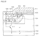
- Fig. 24 shows a section of the voltage-driven thyristor disclosed in the above reference.
- an n-buffer layer 102 is formed on a p+-anode layer 101.
- An anode electrode 112 is formed on the bottom surface of the p+-anode layer 101.
- An n ⁇ -base layer 103 is formed on the n-buffer layer 102.
- P-base layers 104 are formed selectively on the surface of n ⁇ -base layer 103.
- An n+-cathode layer 106 and n-cathode layers 105 are formed on each p-base layer 104.
- n-cathode layers 105 are located at opposite sides of the n+-cathode layer 106.
- On n-cathode layers 105 are formed p+-impurity layers 107 which are also located at opposite sides of n+-cathode layer 106.
- first channel forming regions 113 of a n-channel MOS transistor which will be described later.
- a surface layer of the n-cathode layer 105 adjacent to the first channel forming region 113 forms a second channel forming region 114 of an p-channel MOS transistor, which will be described later.
- a gate electrode 109 is formed on the first and second channel forming regions 113 and 114 with a gate oxide film 108 therebetween.
- the gate electrode 109, p-base layer 104 and p+-impurity layer 107 form a p-channel MOS transistor, of which channel forming region is the second channel forming region 114.
- the gate electrode 109, n ⁇ -base layer 103 and n-cathode layer 105 form the n-channel MOS transistor, of which channel forming region is the first channel forming region 113.
- the gate electrode 109 is covered with a cap oxide film 110.
- Cap oxide film 110 is covered with a cathode electrode 111 which are in contact with n+-cathode layer 106 and p+-impurity layers 107.
- a pnp transistor Tr1 is formed of p+-anode layer 101, n ⁇ -base layer 103, n-buffer layer 102 and p-base layer 104.
- An npn transistor Tr2 is formed of n ⁇ -base layer 103, p-base layer 104 and n+-cathode layer 106.
- a thyristor is formed of the p+-anode layer 101, n-buffer layer 102, n ⁇ -base layer 103, p-base layer 104 and n+-cathode layer 106.
- a p-channel MOS transistor M2 is formed of gate electrode 109, p+-impurity layer 107 and p-base layer 104.
- An n-channel MOS transistor M1 is formed of n-cathode layer 105, gate electrode 109 and n ⁇ -base layer 103.
- the on-state is attained when a positive voltage is applied to anode electrode 112 against cathode electrode 111 and a positive voltage is applied to the gate electrode 109.
- a positive voltage which is not lower than a threshold voltage of the transistor M1
- gate electrode 109 By applying the positive voltage, which is not lower than a threshold voltage of the transistor M1, to gate electrode 109, n-channel MOS transistor M1 is turned on. Thereby, electrons flow into n ⁇ -base layer 103 through the channel of transistor M1, and thus pnp transistor Tr1 is turned on. Thereby, holes flow into p-base layer 104 from the p+-anode layer 101, so that npn transistor Tr2 is also turned on. Consequently, the thyristor formed of transistors Tr1 and Tr2 is turned on. Thus, the main current flows between anode electrode 112 and cathode electrode 111.
- the off-state of the thyristor is attained by applying a negative voltage to gate electrode 109.
- MOS transistor M1 is turned off and p-channel MOS transistor M2 is turned on by applying a negative voltage (not higher than the threshold voltage of p-channel MOS transistor M2) to gate electrode 109.
- a negative voltage not higher than the threshold voltage of p-channel MOS transistor M2
- holes are drawn from p-base layer 104. Consequently, a depletion layer spreads at the junction portion between p-base layer 104 and n ⁇ -base layer 103, so that holes do not flow from the p+-anode layer 101 into p-base layer 104, whereby the off-state of the thyristor is attained.
- Fig. 26 is a schematic diagram showing the problem of the conventional voltage-driven thyristor.
- an inverted layer is formed at the second channel forming region 114 when the thyristor is in the off-state.
- This inverted layer is formed only at the position directly under gate electrode 109. Therefore, all the holes to be drawn from p-base layer 104 must move up to the second channel forming region 114.
- the holes existing at the portion remote from the second channel forming region 114 flows through the second channel forming region 114 into p+-impurity layer 107. Therefore, the holes, which existed at the position remote from the second channel forming region 114, move a long distance before reaching the channel forming region 114. This increases a resistance against the holes being drawn, resulting in such a problem that a long time is required for setting the thyristor to the off-state. Also, the increased resistance against the holes being drawn disadvantageously reduces a magnitude of the main current which can be interrupted.
- a voltage-driven thyristor disclosed in Japanese Patent Laying-Open No. 60-253275.
- Fig. 27 is a cross section showing the voltage-driven thyristor disclosed in Japanese Patent Laying-Open No. 60-253275.
- the voltage-driven thyristor is provided with deep first V-grooves 115a (only one is shown in the figure) for turning on the thyristor and shallow second V-grooves 115b for turning off the thyristor.
- a first gate electrode 109a is formed on the inner surface of each first V-groove 115a with the gate oxide film 108 therebetween.
- a second gate electrode 109b is formed on the inner surface of each second V-groove 115b with the gate oxide film 108 therebetween.
- the voltage-driven thyristor disclosed in Japanese Patent Laying-Open No. 60-253275 has such features that there are provided two kinds of grooves, i.e., deep first V-grooves 115a and shallow second V-grooves 115b, and that the deep first V-grooves 115a are small in number than the shallow second V-grooves 115b.
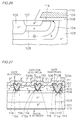
- Fig. 28 is a schematic diagram for showing an advantage of the improved voltage-driven thyristor.
- the thyristor is turned on by applying a positive potential to the first gate electrode 109a. Thereby, electrons flow through the first channel forming regions 113 into n ⁇ -base layer 103. Thereby, the thyristor is turned on in a manner similar to the voltage-driven thyristor already described with reference to Figs. 24 and 25.
- the thyristor is turned off by applying a negative voltage to the first and second gate electrodes 109a and 109b.
- a negative voltage is applied to the first and second gate electrodes 109a and 109b, inverted layers are formed at the second channel forming regions 114.
- the thyristor is turned off in a manner similar to the conventional voltage-driven thyristor already described with reference to Figs. 24 and 25.
- the second channel forming regions 114 are formed in a longitudinal direction and located near p-base layer 104. This reduces a resistance against holes being drawn from p-base layer 104. This results in an advantage that a time for setting the thyristor to the off-state is short. Also, a magnitude of the interruptible main current can be increased owing to the small resistance against holes being drawn from p-base layer 104.
- Fig. 29 is a schematic cross section for showing the first problem of the above improvement.
- an inverted layer is formed in the first channel forming region 113 at each side wall of the first V-groove 115a, and electrons flow from n-cathode layer 105 into n ⁇ -base layer 103. These electrons flow into p+-anode layer 101. Holes are fed into the n ⁇ -base layer 103 through the same path as the electrons flowing into p+-anode layer 101.
- This improvement is designed to include a relatively small number of first V-grooves 115a.
- Fig. 30 is an enlarged cross section of the first V-groove 115a for showing the second problem.
- the first V-groove 115a has a bottom reaching n ⁇ -base layer 103.
- a bottom end region 116 of the first V-groove 115a is located in n ⁇ -base layer 103. Therefore, an electric field is likely to concentrate at the vicinity of end region 116a. This likely results in breakage of the pn junction near end region 116 and thus flow of a leak current near end region 116. As a result, the thyristor may shift to the off-state due to the leak current even if the thyristor is to be held in the off-state. Thus, the reliability may decrease.
- Another object of the invention is to provide a voltage-driven thyristor having high breakdown voltage as well as a method of manufacturing the same.
- a voltage-driven thyristor includes a first semiconductor layer of a first conductivity type, a second semiconductor layer of a second conductivity type, a third semiconductor layer of the first conductivity type, a fourth semiconductor layer of the second conductivity type, a fifth semiconductor layer of the first conductivity type, a plurality of first and second trenches, a plurality of first and second gate electrodes, a cathode electrode and an anode electrode.
- the second semiconductor layer is formed on the first semiconductor layer.
- the third semiconductor layer is formed on the second semiconductor layer.
- the fourth semiconductor layer is formed on the third semiconductor layer.
- the fifth semiconductor layer is selectively formed on a surface of the fourth semiconductor layer.
- the first trenches are formed through the fourth and third semiconductor layers and reach the second semiconductor layer.
- the second trenches are formed through the fifth and fourth semiconductor layers and have bottom surfaces located in the third semiconductor layer.
- the first and second trenches are disposed alternately.
- the first and second gate electrodes are formed in the first and second trenches, respectively.
- the cathode electrode is formed on the fourth and fifth semiconductor layers.
- the anode electrode is formed on a lower surface of the first semiconductor layer.
- the first and second trenches are disposed alternately. Therefore, the first trenches can be substantially equal in number to the second trenches.
- the improvement in the prior art described before has the problem relating to setting of the voltage-driven thyristor to the on-state due to the fact that V-grooves 115a for turning on the voltage-driven thyristor are small in number.
- a rate of the first trenches, which contribute to the setting of the voltage-driven thyristor to the on-state is increased, so that carries can be efficiently supplied into the second semiconductor layer. Therefore, a time required for setting the voltage-driven thyristor to the on-sate can be reduced.
- the first gate electrodes can be disposed regularly at a high density. Accordingly, carriers can be supplied efficiently and uniformly into the second semiconductor layer from the first semiconductor layer. This also contributes to reduction of the time required for setting the voltage-driven thyristor to the on-state.
- a junction portion between the third and second semiconductor layers is constant in depth from an upper surface of the fifth semiconductor layer.
- the voltage-driven thyristor of the second aspect is not provided with a second region, which is provided in a voltage-driven thyristor of an twelfth aspect. Therefore, the first and second trenches can be arranged at a higher density. This enables more quick setting of the voltage-driven thyristor to the on-state.
- the third semiconductor layer has a first region and a second region.
- the first region has a first junction portion joining to the second semiconductor layer and located at a first depth from the upper surface of the fifth semiconductor layer.
- the second region has a second junction portion joining to the second semiconductor layer and located at a second depth from the upper surface of the fifth semiconductor layer, which is larger than the first depth.
- the first trenches are located through the first region, and the second trenches have bottom surfaces located in the second region.
- the fifth semiconductor layer is selectively formed along a longitudinal direction of the first and second trenches.
- the fourth semiconductor layer exists between the fifth semiconductor layers.
- a concentration of impurities of the second conductivity type contained in the fourth semiconductor layer existing between the fifth semiconductor layers is higher than a that of the fourth semiconductor layer underlying the fifth semiconductor layer.
- the fifth semiconductor layer extends parallel to the second trench and along a side wall of the second trench.
- a surface layer of the fourth semiconductor layer extends parallel to the first trench and along a side wall of the first trench.
- a density of a region in the fourth semiconductor layer adjoining to the side wall of the first trench is high.
- the density of impurities is high at the region through which a main current flows during the on-state of the voltage-driven thyristor.
- the fifth semiconductor layer extends parallel to the second trench and along a side wall of the second trench.
- the fifth semiconductor layer has a local portion reaching a side wall of the first trench.
- the fifth semiconductor layer has the local portion reaching the side wall of the first trench.
- a surface layer of the fourth semiconductor layer extends parallel to the first trench and along a side wall of the first trench.
- the fourth semiconductor layer is provided at its surface layer with a local portion reaching a side wall of the second trench.
- the fourth semiconductor layer has the local portion reaching the side wall of the second trench.
- the voltage-driven thyristor can smoothly shift to the on-state.
- a contact area between the fourth semiconductor layer and the cathode electrode can be increased. Therefore, it is possible to increase a current flowing through the voltage-driven thyristor.
- a concentration of impurities of the first conductivity type contained in a first region of the third semiconductor layer adjoining to a side wall of the first trench is lower than that of a second region of the third semiconductor layer adjoining to a side wall of the second trench.
- the density of the second region of the third semiconductor layer adjoining to the side wall of the second trench is higher than that of the first region of the third semiconductor layer adjoining to the side wall of the first trench.
- a channel of an MOS transistor, which operates as a major component for setting the voltage-driven thyristor to the off-state, is formed on this second region. Therefore, carriers can be efficiently supplied to the above channel when the voltage-driven thyristor shifts to the off-state. Therefore, the voltage-driven thyristor can quickly shift to the off-state.
- the third semiconductor layer has a third region of the first conductivity type which has a portion located under the second trench and protrudes into the second semiconductor layer.
- a concentration of impurities of the first conductivity type contained in the second region is higher than that of impurities of the first conductivity type contained in the third region.
- a junction portion between the third region and the second semiconductor layer is located at a position deeper than that of a bottom surface of the first trench.
- a voltage-driven thyristor includes a first semiconductor layer of a first conductivity type, a second semiconductor layer of a second conductivity type, a third semiconductor layer of the first conductivity type, a fourth semiconductor layer of the second conductivity type, a fifth semiconductor layer of the first conductivity type, first and second trenches, first and second gate electrodes, a cathode electrode and an anode electrode.
- the second semiconductor layer is formed on the first semiconductor layer.
- the third semiconductor layer is formed on the second semiconductor layer.
- the fourth semiconductor layer is formed on the third semiconductor layer.
- the fifth semiconductor layer is selectively formed in a surface of the fourth semiconductor layer.
- the third semiconductor layer includes a first region, which has a first junction portion joining to the second semiconductor layer and located at a first depth from an upper surface of the fifth semiconductor layer, and a second region, which has a second junction portion joining to the second semiconductor layer and located at a second depth larger than the first depth from the upper surface of the fifth semiconductor layer.
- the first trench is formed through the fourth semiconductor layer and the first region, and reaches the second semiconductor layer.
- the second trench is formed through the fourth and fifth semiconductor layers and has a bottom surface located in the second region.
- the first and second gate electrodes are formed in the first and second trenches, respectively.
- the cathode electrode is formed on the fourth and fifth semiconductor layers.
- the anode electrode is formed on a lower surface of the first semiconductor layer.
- the second junction portion is formed at a deep position. Therefore, a depletion layer can spread to cover a bottom of the first trench protruding into the second semiconductor layer when the voltage-driven thyristor is in the off-state. Therefore, a bottom edge of the first trench is located in the depletion layer. Meanwhile, in the depletion layer a uniform electric field is applied. Owing to the fact that the bottom edge of the first trench is located in the depletion layer, it is possible to prevent effectively the concentration of the electric field at the edge of the first trench. Thus, the reliability of the voltage-driven thyristor can be improved.
- the second junction portion is located at a position deeper than the first trench. Therefore, the depletion layer can cover more surely the bottom edge of the first trench when the voltage-driven thyristor is turned on.
- a concentration of impurities of the first conductivity type contained in the second region is higher than that of impurities of the first conductivity type contained in the first region.
- the concentration of impurities of the first conductivity type contained in the second region is higher than that of impurities of the first conductivity type contained in the first region.
- the second region is located under the second trench.
- an inverted layer is formed in the fourth semiconductor layer adjoining to a side wall of the second trench.
- a region in which the inverted layer is formed is located above the second region.
- a pair of the second regions are formed at opposite sides of the first region.
- the first trench is formed through the first region, and a pair of the second trenches have bottom surfaces located in a pair of the second regions.
- the voltage-driven thyristor of the fifteenth aspect since the second regions are formed at opposite sides of the first region, a depletion layer can easily cover a bottom edge of the first trench. Therefore, the voltage-driven thyristor can have improved reliability.
- a plurality of first trenches are formed between a pair of second regions.
- a plurality of the first trenches are formed between the second regions, in which case bottom edges of first trenches can be covered with a depletion layer by appropriately adjusting a depth at which the second regions are formed. Therefore, similarly to the above case, the voltage-driven thyristor can have improved reliability.
- a voltage-driven thyristor includes an anode layer of a first conductivity type, a first base layer of a second conductivity type, a second base layer of the first conductivity type, a cathode layer of the second conductivity type, an impurity layer of the first conductivity type, a plurality of first and second trenches, a plurality of on-gates, a plurality of off-gates, a cathode electrode and an anode electrode.
- the first base layer is formed on the anode layer.
- the second base layer is formed on the first base layer.
- the cathode layer is formed on the second base layer.
- the impurity layer is selectively formed in a surface of the cathode layer.
- the first trenches are formed through the cathode layer and the second base layer and reaches the first base layer.
- the second trenches are disposed alternately to the first trenches, and are formed through the impurity layer and the cathode layer with their bottom surfaces located in the second base layer.
- the on-gates are formed in the first trenches.
- the off-gates are formed in the second trenches.
- the cathode electrode is formed on the cathode layer and a surface of the impurity layer.
- the anode electrode is formed on a lower surface of the anode layer.
- the on-gates and the off-gates are disposed alternately. Therefore, a rate of the on-gates can be larger than that in the prior art improvement already described. This enables more uniform and efficient supply of carriers from the collector layer into the first base layer. This enables reduction of a time required for setting the voltage-driven thyristor to the on-state.
- a second semiconductor layer of a second conductivity type is formed on a first semiconductor layer of a first conductivity type. Impurities of the first conductivity type are introduced into a surface of the second semiconductor layer to form a third semiconductor layer of the first conductivity type. Impurities of the second conductivity type are introduced into a whole surface of the third semiconductor layer to form a fourth semiconductor layer of the second conductivity type. Impurities of the first conductivity type are selectively introduced into a surface of the fourth semiconductor layer to form a fifth semiconductor layer. First and second trenches are formed. The first trench extends through the fifth and fourth semiconductor layers and has a bottom surface located in the third semiconductor layer.
- the second trench extends up to the second semiconductor layer through the fifth, fourth and third semiconductor layers.
- First and second gate electrodes are formed on inner surfaces of the first and second trenches with insulating films therebetween, respectively.
- An insulating layer is formed on the first and second gate electrodes.
- a cathode electrode is formed on a surface of the fifth semiconductor layer and a portion of the surface of the fourth semiconductor layer.
- An anode electrode is formed on a lower surface of the first semiconductor layer.
- the method of manufacturing the voltage-driven thyristor of a nineteenth aspect is premised on that the third semiconductor layer includes first and second regions.
- the first region has a first diffusion depth from the surface of the third semiconductor layer.
- the second region has a second diffusion depth from the surface of the third semiconductor layer which is smaller than the first diffusion depth.
- the step of forming the third semiconductor layer includes the steps of selectively introducing impurities of the first conductivity type into the surface of the second semiconductor layer and thereby effecting a diffusion process for forming the first region, and introducing impurities of the first conductivity type into the whole surface of the second semiconductor layer and diffuse the impurity of the first conductivity type up to the second diffusion depth for forming the second region.
- the impurity layer (a first region) and the third layer (a second region) are formed at different steps.
- a concentration of impurities can be high regardless of a concentration of the third semiconductor layer. Therefore, a high impurity concentration region can be formed under the first trench. This can enhance an efficiency with which carries are supplied to a channel of an MOS transistor operating as a major component for setting the voltage-driven thyristor to the off-state. Thereby, it is possible to reduce a time required for setting the voltage-driven thyristor to the off-state.
- the third semiconductor layer is formed to have a uniform depth by introducing impurities of the first conductivity type into the whole surface of the second semiconductor layer and effecting a diffusion process.
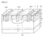
- Fig. 1 is a perspective view partly in section showing a voltage-driven thyristor of the first embodiment of the invention.
- an n-buffer layer 2 is formed on a p+-anode layer 1.
- An anode electrode 12 is formed on the lower surface of the p+-anode layer 1.
- the anode electrode 12 may be made of metal such as aluminum.
- n ⁇ -base layer 3 is formed on n-buffer layer 2. On n ⁇ -base layer 3, there are formed a p-base layer 4 and a p-type impurity layer 4a. An n-cathode layer 5 is formed on p-base layer 4. On a surface of n-cathode layer 5, there are selectively formed n+-cathode layers 6 as well as p+-impurity layers 7.
- first trenches 16a of a depth D which extend through p+-impurity layer 7, n-cathode layer 5, n+-cathode layer 6 and p-base layer 4 into base layer 3.
- a first gate electrode (turn-on gate) 9a is formed on an inner surface of each first trench 16a with a gate oxide film 8 therebetween.
- second trenches 16b of a depth D which extend through p+-impurity layer 7, n-cathode layer 5 and n+-cathode layer 6 and have bottom surfaces located in p-type impurity layer 4a.
- a second gate electrode 9b is formed on an inner surface of each second trench 16b with the gate oxide film 8 therebetween.
- Second and first gate electrodes 9b and 9a may be made of polysilicon containing impurity introduced thereinto.
- First and second gate electrodes 9a and 9b are electrically connected at the end of trenches.
- Cap oxide films 10 are formed on the first and second gate electrodes 9a and 9b.
- a cathode electrode 11 is formed on cap oxide films 10, p+-impurity layers 7 and n+-cathode layers 6.
- Cathode electrode 11 may be made of metal such as aluminum.
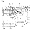
- FIG. 2 shows an operation principle of the voltage-driven thyristor of the first embodiment described above.
- the on-state will first be described below with reference to Fig. 2.
- a positive voltage is applied to first and second gate electrodes 9a and 9b.
- an n-channel MOS transistor near the side wall of first trench 16a is turned on, so that a current Ie flows in the n-channel MOS transistor.
- electrons flow into n ⁇ -base layer 3 through this n-channel MOS transistor.
- a pnp transistor Tr1 is turned on, and a current I A flows through pnp transistor Tr1.
- an npn transistor Tr2 is also turned on, so that a current I k flows. Owing to the turn-on of the pnp transistor Tr1 and npn transistor Tr2 in this manner, the thyristor is turned on, so that the main current flows through the voltage-driven thyristor.
- the off-state is attained by applying a negative potential to first and second gate electrodes 9a and 9b.
- the negative voltage By application of the negative voltage to the first and second gate electrodes 9a and 9b, the n-channel MOS transistor near the side wall of first trench 16a is turned off, and the p-channel MOS transistor near the side wall of second trench 16b is turned on. Thereby, holes are drawn from p-base layer 4. Consequently, a depletion layer spreads in the junction portion between p-base layer 4 n ⁇ -base layer 3, so that the voltage-driven thyristor is shifted to the off-state.
- FIGs. 3 and 4 are cross sections schematically showing a distinctive operation of the voltage-driven thyristor of the first embodiment.
- p-type impurity layer 4a is formed under second trenches 16b. P-type impurity layer 4a is protruded into n ⁇ -base layer 3. A depth of p-type impurity layer 4a is preferably larger than a depth of first trench 16a.
- Fig. 3 shows a state where the voltage-driven thyristor is turned off and a depletion layer 17 spreads into the junction boundary between p-type impurity layer 4a and n ⁇ -base layer 3 and between p-base layer 4 and n ⁇ -base layer 3.
- P-type impurity layer 4a is deep and protruded into n ⁇ -base layer 3 as shown in Fig.
- depletion layer 17 can spread into a deep position. Thereby, depletion layer 17 can cover the bottom edges of first trench 16a deeply. Therefore, concentration of an electric field at the bottom edges of first trench 16a can be effectively prevented. Therefore, the voltage-driven thyristor can have a high reliability.
- depletion layer 17 can be formed at a deep position under first trench 16a.
- the voltage-driven thyristor can have high reliability similarly to the case described before.
- one first trench 16a is formed between the adjacent trenches 16b.
- two or more first trenches 16a may be formed between second trenches 16b.
- p-type impurity layers 4a are formed at an appropriate depth so that depletion layer 17 can cover the bottom edges of these first trenches 16a. Thereby, the voltage-driven thyristor with high reliability is obtained.
- inverted layers are formed at second channel forming regions 14. Holes are drawn through second channel forming regions 14 from p-base layer 4 and p-type impurity layer 4a into p+-impurity layer 7.
- p-base layer 4 located immediately under second channel forming region 14 has the highest concentration of impurities according to the structure of the first embodiment shown in Fig. 3.
- first trenches 16a and second trenches 16b are formed alternately in the voltage-driven thyristor of the first embodiment shown in Fig. 1. This arrangement enables quick setting of the voltage-driven thyristor to the on-state.
- Fig. 4 holes are supplied from p+-anode layer 1 to n ⁇ -base layer 3 through the same position or path in the p+-anode layer 1 as that through which electrons move into the p+-anode layer 1. These electrons have been injected into n ⁇ -base layer 3 through the channel region of the n-channel MOS transistor formed at the side wall of first trench 16a. Since the voltage-driven thyristor of the first embodiment shown in Fig. 4 is provided with first and second trenches 16a and 16b which are formed alternately, a degree of integration of the n-channel MOS transistors can be higher than that of the conventional improvement shown in Fig. 29.
- the high degree of integration of the n-channel MOS transistors enables a number of positions through which holes are supplied from p+-anode layer 1 into n ⁇ -base layer 3. Thereby, holes can be supplied efficiently from p+-anode layer 1 into n ⁇ -base layer 3. Therefore, a time required for setting the voltage-driven thyristor to the on-state can be shorter than that of the conventional improvement described before.
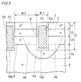
- a structure near the second trench 16b will be described below in greater detail. Numerical limits which will be described below are premised on that a breakdown voltage of the voltage-driven thyristor is in a range from about 400V to about 500V.
- Fig. 5 is an enlarged cross section showing a structure of and around second trench 16b.
- an open width W1 of second trench 16b is about 1 ⁇ m.
- a diffusion depth D1 of p+-impurity layer 7 is preferably not more than about 1 ⁇ m.
- a diffusion depth D2 of n-cathode layer 5 is preferably about 1.5 ⁇ m.
- a diffusion depth D3 of p-base layer 4 is preferably in a range from about 1.5 ⁇ m to about 2 ⁇ m.
- a diffusion depth D4 of p-type impurity layer 4a is preferably in a range from about 2 ⁇ m to about 3 ⁇ m. In this case, a diffusion depth of p-type impurity layer 4a from the upper surface of impurity layer 7 is in a range from about 6 ⁇ m to about 7 ⁇ m.
- First and second trenches 16a and 16b preferably have a depth in a range from about 5 ⁇ m to about 6 ⁇ m. Also, a distance W2 between first and second trenches 16a and 16b is in a range from about 5 ⁇ m to about 10 ⁇ m. The reason of this is that p-type impurity for p-type impurity layer 4a is diffused into a deep position and hence the p-type impurity spreads also in a lateral direction.
- a concentration of p-base layer 4 is approximately in a range from 1016cm ⁇ 3 to 1017cm ⁇ 3. This range is determined based on a threshold voltage Vth of the n-channel MOS transistor formed at the side wall of first trench 16a.
- a concentration of p-type impurity layer 4a is approximately in a range from 1016cm ⁇ 3 to 1018cm ⁇ 3 or more. Thereby, the region 4b at which p-base layer 4 and p-type impurity layer 4a overlap with each other has the highest concentration in a range from 2x1016cm ⁇ 3 to 1018cm ⁇ 3.
- This region 4b is located immediately under the channel forming region of the p-channel MOS transistor which operates as a major component when the voltage-driven thyristor is set to the off-state. Therefore, holes can be supplied efficiently to the p-channel MOS transistor.
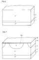
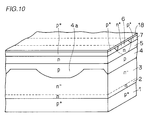
- Figs. 6 to 10 are perspective views showing 1st to 5th steps in a process of manufacturing the voltage-driven thyristor of the first embodiment, respectively.
- Figs. 11A and 11B are perspective views showing modifications of a formation pattern of p+-impurity layers 7.
- Figs. 12 to 17 are perspective views showing 6th to 11th steps in a process of manufacturing the voltage-driven thyristor of the first embodiment.
- the voltage-driven thyristor completed through the manufacturing process which will be described below has, for example, the structure including relatively large cap oxide films 10 as shown in Fig. 17. Cap oxide films 10 partially fill first and second trenches or grooves 16a and 16b so as to complete the voltage-driven thyristor of the first embodiment shown in Fig. 1.
- n-buffer layer 2 and n ⁇ -base layer 3 are successively formed on the p+-anode layer 1 by an epitaxial growth method. Then, referring to Fig. 7, an oxide film 18 is formed on the surface of n ⁇ -base layer 3.
- p-type impurities are selectively introduced into n ⁇ -base layer 3, for example, by the ion implantation or diffusion from gas.
- a thermal diffusion process is effected to form p-type impurity layer 4a preferably at a concentration of about 1016/cm3 to 1018/cm3.
- p-type impurities are introduced through oxide film 18 into the whole surface of n ⁇ -base layer 3.
- a thermal diffusion process is effected to form p-base layer 4 preferably at a concentration of about 1016/cm3 to 1017/cm3.
- P-base layer 4 thus formed has a diffusion depth smaller than that of p-type impurity layer 4a.
- p-base layer 4 and p-type impurity layer 4a are formed at different steps, so that it is possible to form the high concentration region at which p-base layer 4 and p-type impurity layer 4a overlap with each other.
- the side wall of second trench 16b is partially formed in this high impurity concentration region. Thereby, it is possible to increase the concentration of p-type impurities in p-base layer 4 near the side wall of second trench 16b. Therefore, it is possible to improve the turn-off characteristics of the voltage-driven thyristor.
- n-type impurities are introduced into the whole surface of p-base layer 4. Then, a thermal diffusion process is effected to form n-cathode layer 5.
- n-type impurities and p-type impurities are selectively introduced into the surface of n-cathode layer 5 to form n+-cathode layers 6 and p+-impurity layers 7, respectively.
- N+-cathode layers 6 thus formed may be deep enough to reach the upper surface of p-base layer 4.
- various pattern structures of p+-impurity layers 7 and n+-cathode layers 6 may be selected in accordance with required characteristics of a device.
- oxide films 19 of a predetermined thickness are formed on p+-impurity layers 7 and n+-cathode layers 6. Using oxide films 19 as a mask, etching is effected to form first and second trenches 16a and 16b. In this embodiment, since first and second trenches 16a and 16b have the same depth, they can be formed simultaneously. Thereby, the process is simplified.
- a thermal oxidation method or a CVD method is used to form gate oxide films 8 in first and second trenches 16a and 16b.
- a polysilicon layer is deposited on oxide films 19.
- the polysilicon layer has a thickness enough to fill first and second trenches 16a and 16b and contains impurity doped therein.
- An etch-back process is effected on the polysilicon layer to form polysilicon layers 9a and 9b filling first and second trenches 16a and 16b as shown in Fig. 14. In this manner, first and second gate electrodes 9a and 9b are formed.
- Above polysilicon layer is left at the end of first and second trenches 16a and 16b to electrically connect first and second gate electrodes 9a and 9b.
- the thermal oxidation method, CVD method or the like is used to form oxide films 10a.
- the CVD method is used to form cap oxide film 10 on oxide films 10a and 19.
- the cap oxide films 10 and 19 are patterned to expose the surfaces of p+-impurity layers 7 and n+-cathode layers 6 while partially remaining oxide films 19 and cap oxide films 10 on first and second gate electrodes.
- a sputtering method or the like is used to form cathode electrode 11 on oxide films 10, p+-impurity layers 7 and n+-cathode layers 6.
- the anode electrode 12 is formed on the lower surface of the p+-anode layer 1.
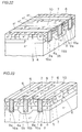
- FIG. 18 is a perspective view of the voltage-driven thyristor of the second embodiment of the invention.
- the second embodiment is not provided with p-type impurity layer 4a in contrast to the first embodiment already described. Therefore, The junction portion between p-base layer 4 and n ⁇ -base layer 3 is spaced by a substantially constant distance from the surfaces of p+-impurity layers 7 and n+-cathode layers 6. Naturally, the step of forming the p-type impurity layer 4a is not required. Thus, p-base layer 4 is formed by introducing p-type impurities into the whole surface of n ⁇ -base layer 3.
- first trench 16a has a depth D5 larger than a depth D6 of second trench 16b. Therefore, first gate electrode 9a formed in first trench 16a functions as a turn-on gate, and second gate electrode 9b formed in second trench 16b functions as a turn-off gate.
- Other structures are the same as those of the voltage-driven thyristor of the first embodiment shown in Fig. 1. Since first and second trenches 16a and 16b have different depths, they are formed at different steps.
- a space between first and second trenches 16a and 16b can be smaller than that in the first embodiment. Therefore, a degree of integration of first and second trenches can be increased. Consequently, a time for setting the voltage-driven thyristor to the turn-on state can be further reduced to a value smaller than that in the first embodiment.
- first and second trenches 16a and 16b are spaced from each other by the relatively large distance W2 of about 5 to 10 ⁇ m.
- the second embodiment is not provided with p-type impurity layer 4a as can be seen from Fig. 19, so that the degree of integration of first and second trenches 16a and 16b can be increased. More specifically, a distance W3 between first and second trenches 16a and 16b can be a small value of about 2 to 3 ⁇ m. Therefore, it is possible to increase the degree of integration of the n-channel MOS transistors formed at the side walls of first trenches 16a. Accordingly, the time required for setting the voltage-driven thyristor to the on-state can be further reduced to a value smaller than that in the first embodiment.
- Fig. 20 is a perspective view showing a first modification of the pattern of p+-impurity layer 7 and n+-cathode layer 6.
- each n+-cathode layer 6 has a bottom at a deep position which reaches the upper surface of p-base layer 4.
- Other structures are the same as those of the voltage-driven thyristor of the first embodiment shown in Fig. 1.
- each n+-cathode layer 6 is elongated parallel to the longitudinal direction of first trench 16a. Therefore, the inverted layer of the n-channel MOS transistor is continuously formed along the side wall of first trench 16a during setting to the on-state. As a result, the on-current can flow to the cathode electrode through the channel more efficiently than the first modification.
- N+-cathode layer 6 has the bottom at a deep position which reaches the upper surface of p-base layer 4. Therefore, it is possible to reduce a resistance against a main current flowing through cathode layer 6 during the on-state of the voltage-driven thyristor. Accordingly, a large current can flow through the voltage-driven thyristor.
- P+-impurity layer 7 is continuously elongated parallel to the side wall of the second trench 16b.
- Fig. 22 is a perspective view showing a voltage-driven thyristor of the third modification. Referring to Fig. 22, this modification is preferably employed in the case where, rather than turn-on characteristics, intended turn-off characteristics are to be ensured.
- p+-impurity layer 7 extends along the side wall of second trench 16b.
- P+-impurity layer 7 has local portions reaching the side wall of first trench 16a. Therefore, n+-cathode layers 6 are formed selectively and intermittently along the side wall of first trench 16a.
- p+-impurity layer 7 extends along second trench 16b and has the local portions reaching the side wall of both first and second trenches 16a and 16b, it is possible to increase a channel width of the p-channel transistor (i.e., transistor functioning as a major component when turning off the voltage-driven thyristor) compared with the case of the second modification described before. Therefore, the voltage-driven thyristor can be set to the off-state more quickly and surely than that of the second modification.
- FIG. 23 is a perspective view showing a voltage-driven thyristor of the fourth modification.
- This modification is preferably employed in the case where, rather than turn-off characteristics, intended turn-on characteristics are to be ensured.
- n+-cathode layer 6 is continuously formed along each side wall of first trench 16a, and has local portions reaching the side wall of second trench 16b. Thereby, it is possible to increase a contact area between the cathode electrode and n+-cathode layer 6. Therefore, it is possible to reduce a resistance against the main current flowing through cathode layer 6 during the on-state of the voltage-driven thyristor. This enables the structure in which a large current can be easily obtained.
- P+-impurity layers 7 are formed selectively and intermittently along each side wall of second trench 16b.
- the third semiconductor layer is provided with the second region, so that concentration of the electric field at the bottom edge of the first trench can be prevented effectively. Therefore, the voltage-driven thyristor can have high reliability.
- the concentration of impurities of the first conductivity type contained in the second region of the third semiconductor layer is larger than the concentration of impurities of the first conductivity type contained in the first region of the third semiconductor layer, whereby carriers can be supplied efficiently to the MOS transistor which operates when setting the voltage-driven thyristor to the off-state. Therefore, it is possible to reduce the time required for setting the voltage-driven thyristor to the off-state and to turn the voltage-driven thyristor off even a large current. Thus, the voltage-driven thyristor can have superior turn-off characteristics.
- the bottom edge of the first trench can be covered with the depletion layer spreading at the junction between the third and second semiconductor layers when the voltage-driven thyristor is in the off-state. Therefore, the voltage-driven thyristor can have improved reliability.
- the impurity concentration of the first region in the third semiconductor layer adjoining to the side wall of the first trench is lower than the impurity concentration of the second region in the third semiconductor layer adjoining to the side wall of the second trench, so that carries can be supplied efficiently to the channel region of the MOS transistor which operates as a major component when the voltage-driven thyristor is set to the off-state. Therefore, it is possible to reduce the time required for setting the voltage-driven thyristor to the off-state. Thus, the voltage-driven thyristor can have superior turn-off characteristics.
- the impurity layer of the first conductivity type and the third semiconductor layer are formed at different steps, so that it is possible to increase an impurity concentration of the impurity layer regardless of the impurity concentration of the third semiconductor layer.
- the region, which is formed in the impurity layer and adjoins to the side wall of the first trench, has a high impurity concentration. Therefore, the voltage-driven thyristor has superior turn-off characteristics.
Landscapes
- Thyristors (AREA)
- Junction Field-Effect Transistors (AREA)
Applications Claiming Priority (3)
| Application Number | Priority Date | Filing Date | Title |
|---|---|---|---|
| JP31504593 | 1993-12-15 | ||
| JP315045/93 | 1993-12-15 | ||
| JP31504593A JP3260944B2 (ja) | 1993-12-15 | 1993-12-15 | 電圧駆動型サイリスタおよびその製造方法 |
Publications (3)
| Publication Number | Publication Date |
|---|---|
| EP0658939A2 true EP0658939A2 (fr) | 1995-06-21 |
| EP0658939A3 EP0658939A3 (fr) | 1999-05-19 |
| EP0658939B1 EP0658939B1 (fr) | 2005-11-30 |
Family
ID=18060770
Family Applications (1)
| Application Number | Title | Priority Date | Filing Date |
|---|---|---|---|
| EP94113791A Expired - Lifetime EP0658939B1 (fr) | 1993-12-15 | 1994-09-02 | Thysistor commandé en tension et procédé de fabrication |
Country Status (7)
| Country | Link |
|---|---|
| US (1) | US5457329A (fr) |
| EP (1) | EP0658939B1 (fr) |
| JP (1) | JP3260944B2 (fr) |
| KR (1) | KR0146640B1 (fr) |
| DE (1) | DE69434562T2 (fr) |
| DK (1) | DK0658939T3 (fr) |
| TW (1) | TW327244B (fr) |
Cited By (1)
| Publication number | Priority date | Publication date | Assignee | Title |
|---|---|---|---|---|
| EP0785582A3 (fr) * | 1996-01-16 | 1999-08-04 | Harris Corporation | Thyristor à contrÔle MOS avec grille dans une tranchée |
Families Citing this family (15)
| Publication number | Priority date | Publication date | Assignee | Title |
|---|---|---|---|---|
| JPH09246523A (ja) * | 1996-03-13 | 1997-09-19 | Mitsubishi Electric Corp | 半導体装置 |
| US6080625A (en) * | 1998-08-26 | 2000-06-27 | Lucent Technologies Inc. | Method for making dual-polysilicon structures in integrated circuits |
| JP3647676B2 (ja) * | 1999-06-30 | 2005-05-18 | 株式会社東芝 | 半導体装置 |
| US6534828B1 (en) * | 2000-09-19 | 2003-03-18 | Fairchild Semiconductor Corporation | Integrated circuit device including a deep well region and associated methods |
| JP4534500B2 (ja) * | 2003-05-14 | 2010-09-01 | 株式会社デンソー | 半導体装置の製造方法 |
| JP4575713B2 (ja) * | 2004-05-31 | 2010-11-04 | 三菱電機株式会社 | 絶縁ゲート型半導体装置 |
| KR100549010B1 (ko) * | 2004-06-17 | 2006-02-02 | 삼성전자주식회사 | 채널부 홀의 일 측벽에 채널 영역을 갖는 트랜지스터의형성방법들 |
| CN103137658A (zh) * | 2011-11-30 | 2013-06-05 | 成都成电知力微电子设计有限公司 | 半导体器件的含导电颗粒的绝缘体与半导体构成的耐压层 |
| US9306048B2 (en) * | 2012-10-01 | 2016-04-05 | Pakal Technologies Llc | Dual depth trench-gated mos-controlled thyristor with well-defined turn-on characteristics |
| JP2015176891A (ja) | 2014-03-13 | 2015-10-05 | 株式会社東芝 | 半導体装置 |
| JP2015177010A (ja) * | 2014-03-14 | 2015-10-05 | 株式会社東芝 | 半導体装置およびその製造方法 |
| JP6830390B2 (ja) * | 2017-03-28 | 2021-02-17 | エイブリック株式会社 | 半導体装置 |
| US11145717B2 (en) * | 2018-10-01 | 2021-10-12 | Pakal Technologies, Inc. | Cellular insulated gate power device with edge design to prevent failure near edge |
| DE102019210681A1 (de) * | 2019-05-31 | 2020-12-03 | Robert Bosch Gmbh | Leistungstransistorzelle und Leistungstransistor |
| CN112750902B (zh) * | 2021-02-05 | 2021-11-02 | 深圳吉华微特电子有限公司 | 一种高抗短路能力的沟槽栅igbt |
Family Cites Families (5)
| Publication number | Priority date | Publication date | Assignee | Title |
|---|---|---|---|---|
| DE3380136D1 (en) * | 1982-04-12 | 1989-08-03 | Gen Electric | Semiconductor device having a diffused region of reduced length and method of fabricating the same |
| EP0159663A3 (fr) * | 1984-04-26 | 1987-09-23 | General Electric Company | Thyristors, transistors à effet de champ à électrode de porte isolée et MOSFETs à haute densité commandés par effet de champ utilisant une structure MOS formée dans une rainure de type V et procédé de fabrication |
| US4760431A (en) * | 1985-09-30 | 1988-07-26 | Kabushiki Kaisha Toshiba | Gate turn-off thyristor with independent turn-on/off controlling transistors |
| JP3119890B2 (ja) * | 1991-04-16 | 2000-12-25 | 株式会社東芝 | 絶縁ゲート付サイリスタ |
| JP2504862B2 (ja) * | 1990-10-08 | 1996-06-05 | 三菱電機株式会社 | 半導体装置及びその製造方法 |
-
1993
- 1993-12-15 JP JP31504593A patent/JP3260944B2/ja not_active Expired - Fee Related
-
1994
- 1994-02-25 TW TW083101610A patent/TW327244B/zh active
- 1994-08-23 US US08/294,708 patent/US5457329A/en not_active Expired - Lifetime
- 1994-09-02 EP EP94113791A patent/EP0658939B1/fr not_active Expired - Lifetime
- 1994-09-02 DK DK94113791T patent/DK0658939T3/da active
- 1994-09-02 DE DE69434562T patent/DE69434562T2/de not_active Expired - Lifetime
- 1994-12-12 KR KR1019940033747A patent/KR0146640B1/ko not_active Expired - Fee Related
Cited By (1)
| Publication number | Priority date | Publication date | Assignee | Title |
|---|---|---|---|---|
| EP0785582A3 (fr) * | 1996-01-16 | 1999-08-04 | Harris Corporation | Thyristor à contrÔle MOS avec grille dans une tranchée |
Also Published As
| Publication number | Publication date |
|---|---|
| EP0658939B1 (fr) | 2005-11-30 |
| US5457329A (en) | 1995-10-10 |
| EP0658939A3 (fr) | 1999-05-19 |
| DK0658939T3 (da) | 2005-12-27 |
| JPH07169941A (ja) | 1995-07-04 |
| TW327244B (en) | 1998-02-21 |
| KR950021736A (ko) | 1995-07-26 |
| JP3260944B2 (ja) | 2002-02-25 |
| KR0146640B1 (ko) | 1998-08-01 |
| DE69434562D1 (de) | 2006-01-05 |
| DE69434562T2 (de) | 2006-08-10 |
Similar Documents
| Publication | Publication Date | Title |
|---|---|---|
| JP4351745B2 (ja) | 半導体装置 | |
| EP0795911B1 (fr) | Dispositif à semiconducteur ayant une grille isolée et procédé pour sa fabrication | |
| US6359306B1 (en) | Semiconductor device and method of manufacturing thereof | |
| EP1158582B1 (fr) | Diode de type pin. | |
| EP1233457B1 (fr) | Dispositif sémi-conducteur à grille isolée et procédé pour sa fabrication | |
| EP0658939B1 (fr) | Thysistor commandé en tension et procédé de fabrication | |
| US7795638B2 (en) | Semiconductor device with a U-shape drift region | |
| US5070377A (en) | Semiconductor device and method of manufacturing the same | |
| JP2004511910A (ja) | トレンチショットキー整流器が組み込まれたトレンチ二重拡散金属酸化膜半導体トランジスタ | |
| EP0837508A2 (fr) | Dispositif semi-conducteur et l'appareil de conversion de puissance électrique de celui-ci | |
| JPH08316479A (ja) | 絶縁ゲート型半導体装置およびその製造方法 | |
| KR100883795B1 (ko) | 대칭적인 트렌치 mosfet 디바이스 및 그 제조 방법 | |
| JP4294117B2 (ja) | Mosコントロールダイオード及びその製造方法 | |
| EP0810671A2 (fr) | Dispositif semi-conducteur de type transistor bipolaire à grille isolée | |
| JPH08139319A (ja) | 半導体装置およびその製造方法 | |
| US5773851A (en) | Semiconductor device and manufacturing method thereof | |
| US6448588B2 (en) | Insulated gate bipolar transistor having high breakdown voltage in reverse blocking mode | |
| JP3409244B2 (ja) | 半導体装置 | |
| EP0540017B1 (fr) | Thyristor à commande de grille de type MOS | |
| US5723349A (en) | Process for manufacturing a high conductivity insulated gate bipolar transistor integrater structure | |
| JP2001274400A (ja) | 半導体装置 | |
| JP4415767B2 (ja) | 絶縁ゲート型半導体素子、及びその製造方法 | |
| US6281546B1 (en) | Insulated gate field effect transistor and manufacturing method of the same | |
| GB2586158A (en) | Semiconductor device and method for producing same | |
| EP0848430A2 (fr) | Transistor bipolaire à grille isolée |
Legal Events
| Date | Code | Title | Description |
|---|---|---|---|
| PUAI | Public reference made under article 153(3) epc to a published international application that has entered the european phase |
Free format text: ORIGINAL CODE: 0009012 |
|
| AK | Designated contracting states |
Kind code of ref document: A2 Designated state(s): DE DK FR GB |
|
| PUAL | Search report despatched |
Free format text: ORIGINAL CODE: 0009013 |
|
| AK | Designated contracting states |
Kind code of ref document: A3 Designated state(s): DE DK FR GB |
|
| 17P | Request for examination filed |
Effective date: 19990428 |
|
| 17Q | First examination report despatched |
Effective date: 20040823 |
|
| GRAP | Despatch of communication of intention to grant a patent |
Free format text: ORIGINAL CODE: EPIDOSNIGR1 |
|
| GRAS | Grant fee paid |
Free format text: ORIGINAL CODE: EPIDOSNIGR3 |
|
| GRAA | (expected) grant |
Free format text: ORIGINAL CODE: 0009210 |
|
| AK | Designated contracting states |
Kind code of ref document: B1 Designated state(s): DE DK FR GB |
|
| REG | Reference to a national code |
Ref country code: GB Ref legal event code: FG4D |
|
| REG | Reference to a national code |
Ref country code: DK Ref legal event code: T3 |
|
| REF | Corresponds to: |
Ref document number: 69434562 Country of ref document: DE Date of ref document: 20060105 Kind code of ref document: P |
|
| RAP2 | Party data changed (patent owner data changed or rights of a patent transferred) |
Owner name: MITSUBISHI DENKI KABUSHIKI KAISHA |
|
| ET | Fr: translation filed | ||
| PLBE | No opposition filed within time limit |
Free format text: ORIGINAL CODE: 0009261 |
|
| STAA | Information on the status of an ep patent application or granted ep patent |
Free format text: STATUS: NO OPPOSITION FILED WITHIN TIME LIMIT |
|
| 26N | No opposition filed |
Effective date: 20060831 |
|
| PGFP | Annual fee paid to national office [announced via postgrant information from national office to epo] |
Ref country code: DK Payment date: 20090914 Year of fee payment: 16 |
|
| PGFP | Annual fee paid to national office [announced via postgrant information from national office to epo] |
Ref country code: GB Payment date: 20090902 Year of fee payment: 16 |
|
| PGFP | Annual fee paid to national office [announced via postgrant information from national office to epo] |
Ref country code: DE Payment date: 20090827 Year of fee payment: 16 |
|
| PGFP | Annual fee paid to national office [announced via postgrant information from national office to epo] |
Ref country code: FR Payment date: 20091012 Year of fee payment: 16 |
|
| GBPC | Gb: european patent ceased through non-payment of renewal fee |
Effective date: 20100902 |
|
| REG | Reference to a national code |
Ref country code: DK Ref legal event code: EBP |
|
| REG | Reference to a national code |
Ref country code: FR Ref legal event code: ST Effective date: 20110531 |
|
| REG | Reference to a national code |
Ref country code: DE Ref legal event code: R119 Ref document number: 69434562 Country of ref document: DE Effective date: 20110401 |
|
| PG25 | Lapsed in a contracting state [announced via postgrant information from national office to epo] |
Ref country code: DE Free format text: LAPSE BECAUSE OF NON-PAYMENT OF DUE FEES Effective date: 20110401 Ref country code: FR Free format text: LAPSE BECAUSE OF NON-PAYMENT OF DUE FEES Effective date: 20100930 |
|
| PG25 | Lapsed in a contracting state [announced via postgrant information from national office to epo] |
Ref country code: GB Free format text: LAPSE BECAUSE OF NON-PAYMENT OF DUE FEES Effective date: 20100902 |
|
| PG25 | Lapsed in a contracting state [announced via postgrant information from national office to epo] |
Ref country code: DK Free format text: LAPSE BECAUSE OF NON-PAYMENT OF DUE FEES Effective date: 20100930 |