EP0660265A2 - Appareil de test d'une image d'un objet à tester - Google Patents
Appareil de test d'une image d'un objet à tester Download PDFInfo
- Publication number
- EP0660265A2 EP0660265A2 EP94118021A EP94118021A EP0660265A2 EP 0660265 A2 EP0660265 A2 EP 0660265A2 EP 94118021 A EP94118021 A EP 94118021A EP 94118021 A EP94118021 A EP 94118021A EP 0660265 A2 EP0660265 A2 EP 0660265A2
- Authority
- EP
- European Patent Office
- Prior art keywords
- brightness
- abnormal brightness
- abnormal
- test object
- threshold
- Prior art date
- Legal status (The legal status is an assumption and is not a legal conclusion. Google has not performed a legal analysis and makes no representation as to the accuracy of the status listed.)
- Granted
Links
Images



Classifications
-
- G—PHYSICS
- G01—MEASURING; TESTING
- G01N—INVESTIGATING OR ANALYSING MATERIALS BY DETERMINING THEIR CHEMICAL OR PHYSICAL PROPERTIES
- G01N21/00—Investigating or analysing materials by the use of optical means, i.e. using sub-millimetre waves, infrared, visible or ultraviolet light
- G01N21/84—Systems specially adapted for particular applications
- G01N21/88—Investigating the presence of flaws or contamination
- G01N21/90—Investigating the presence of flaws or contamination in a container or its contents
- G01N21/909—Investigating the presence of flaws or contamination in a container or its contents in opaque containers or opaque container parts, e.g. cans, tins, caps, labels
Definitions
- the present invention relates to an image testing device equipped with brightness measuring capabilities for testing an image of the inner surface of a cylindrical container as a test object which is transmitted by, for example, a conveyor so that foreign substances, dust, scratches, etc. can be successfully detected if they exist on the surface.
- Figures 1A and 1B show the method of observing a cylindrical container, that is, a test object, which has metallic luster on its inner surface.
- Figure 1A is the top view of the cylindrical container, and Figure 1B is its sectional view.
- 102 is a cylindrical container.
- a ring-shaped illuminator 101 illuminates the cylindrical container 102 from above, and the center axis of the illuminator 101 matches that of the cylindrical container 102.
- the illuminator 101 When a uniform ring-shaped light is provided by the illuminator 101, the light reflects off the inner surface having the metallic luster.
- a brightness pattern concentric light circles
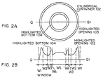
- Figure 1A shows a highlighted portion generated when the light of the illuminator directly reflects off the inner surface of the container. The strongest highlight can be detected around a highlighted opening 103 and a highlighted bottom 104.
- Figure 2A shows a scanning line Q-Q1 passing the center of the container shown in Figure 1A.
- Figure 2B shows a graph of the variation of gray levels inside the container along the scanning line Q-Q1. If the scanning line Q-Q1 is turned round the axis of the container, then a graph can be obtained as shown in Figure 2B.
- the brightness pattern depends on a test object.
- the highlighted portion and a dark portion which is generated when a light does not reflect off the surface toward the viewer, are different in respective cases. However, the feature of generating a concentric bright circle maintains.
- the inner surface of a cylindrical container can be divided into five areas W1 through W5 according to the variation of gray levels.
- the first area W1 refers to the highlighted opening 103.
- the second area W2 refers to the upper portion of the inner side of the container where the variation of gray levels is relatively small.
- the third area W3 receives a small amount of light from the illuminator 101 described by referring to Figure 1, refers to the lower portion of the inner side of the container, and is darker than other portions.
- the fourth area W4 refers to the highlighted bottom 104.
- the fifth area W5 refers to the bottom portion.
- each of these areas W1 through W5 is provided with a window, and a threshold is set to detect a defect indicated by a black spot and a white spot depending on the optical characteristics in each area.
- a method of detecting a defect is, for example, to binarize using a predetermined threshold an 8-bit multivalued gray image signal obtained by A/D converting an analog video signal (analog gray image signal) obtained by scanning an object image; to extract a defect signal by differentiating the video signal by a differentiation circuit as a differentiation method, etc.
- a differentiation signal is issued around the contour of the object.
- the differentiation generates either a forward pulse or a backward pulse around the contour of the object, and generates the forward and backward pulses simultaneously around a small defective portion. Using the above described feature of the differentiation method, a defective portion can be correctly extracted.
- the number of containers of, for example, food is very large per time unit in a checking process. If a defect has been detected in a container tester in a production line, then a quick action should be taken to stop the production line. Otherwise, a large number of defective containers can be produced in a short time, thereby causing a serious problem of recovery of the production line. In this case, a longer recovery time requires a larger amount of financial loss correspondingly.
- an illuminator which is used to stabilize a test image can be an element of the reliability of determination. That is, the brightness of the light of the illuminator may be lowered as time passes, and has undesired influence on precision.
- a test container is captured by a camera using a strobo flashbulb as a light source while it is being conveyed.
- the strobo flashbulb shows an uneven deterioration in brightness and the relationship between the number of flashes and deterioration cannot be calculated exactly.
- a strobo flashbulb is replaced with a new one at predetermined intervals so that the tester can be appropriately maintained.
- the strobo flashbulb costs rather high, and a unit for properly notifying a user of a timely replacement is earnestly demanded.
- a defect can be easily detected, only if the illuminator provides no light at all, by detecting a black spot or a white spot inside a cylindrical container through fixed or difference binarization.
- the tester could recognize all test objects as acceptable containers. In this case, there may arise a serious problem that no correct check is made until an operator recognizes the malfunction of the illuminator.
- the present invention monitors the operation of an illuminator by constantly monitoring the brightness of a test image.
- an abnormal condition exists, it is quickly notified to an external unit to reduce a financial loss in the container production and also to inform a user of a timely replacement for strobo flashbulb of the illuminator.
- the present invention realizes an image testing device to successfully reduce its maintenance cost.
- the image testing device comprises a unit for generating a brightness measure area in an image area of a test object each time it is determined whether or not the test object is a defective product, obtaining the brightness of the picture elements from their average gray level in the brightness measure area, and correcting the binarization threshold, used in detecting a picture element indicating a defective portion of the test object, in proportion to the measured brightness.
- the image testing device also comprises a first abnormal brightness determination unit for determining a preliminary abnormal brightness when the measured brightness is smaller than a predetermined abnormal brightness threshold, and for determining that an abnormal brightness has arisen if the preliminary abnormal brightness has been detected continuously for predetermined times (hereinafter referred to as a continuous abnormal brightness threshold).
- the image testing device also comprises a second abnormal brightness determination unit for determining an abnormal brightness when the frequency of the preliminary abnormal brightness, as an average value of the occurrences of the preliminary abnormal brightness of the test object, is larger than a predetermined threshold. It further comprises an abnormal brightness occurrence signal output unit for outputting an abnormal brightness occurrence signal (for example, an alarm) according to the determination of an occurrence of an abnormal brightness made by both or either of the first and second abnormal brightness determination units.
- a second abnormal brightness determination unit for determining an abnormal brightness when the frequency of the preliminary abnormal brightness, as an average value of the occurrences of the preliminary abnormal brightness of the test object, is larger than a predetermined threshold.
- an abnormal brightness occurrence signal output unit for outputting an abnormal brightness occurrence signal (for example, an alarm) according to the determination of an occurrence of an abnormal brightness made by both or either of the first and second abnormal brightness determination units.
- the image testing device further defines plural sets of the abnormal brightness thresholds and continuous abnormal brightness thresholds, and determines an occurrence of an abnormal brightness made on each set of the abnormal brightness thresholds for each test object by the first and second abnormal brightness determination units.
- the above described abnormal brightness occurrence signal output unit outputs an abnormal brightness occurrence signal variable depending on the level of the deterioration of the intensity of a light source such as a strobo flashbulb.
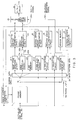
- FIG 3 is a block diagram showing the hardware of the cylindrical container inner surface tester and shows an embodiment of the present invention.
- a multivalued (for example, 8-bit) gray image signal PO is obtained by A/D converting a video signal obtained by raster-scanning the image on a TV camera not shown in Figure 3;
- a frame memory 1 receives and stores the multivalued gray image signal PO as multivalued screen data; and
- an image address generation circuit 3 generates an address of the frame memory 1.
- a window memory 2 stores mask pattern data for each window, that is, various types of ring-shaped window patterns concentric corresponding to the brightness patterns depending on the form of a container.
- a window address generation circuit 4 generates an address of the window memory 2.
- the window gate circuit 5E masks the multivalued gray image signal PO or a multivalued gray image signal 1a read from the frame memory 1 with mask pattern data 2a so that only a specified multivalued gray image signal PO or 1a can be selectively passed.
- Image edge detection circuits 6-1 and 6-2 detect the edges of an image, that is, the outer contour (outer circumference) and the inner contour (inner circumference) of a ring-shaped highlighted opening.
- An input image signal is binarized using a predetermined threshold used to detect the position of a test image and to check the circularity of the contour of a container.
- the coordinates of the rise and fall points (referring to image edges) of the binarized signal are stored in the memories of the image edge detection circuits 6-1 and 6-2.
- a highlighted portion determination circuit 11 checks the circularity of the contour of a container with reference to the outer or inner circumference detected by the image edge detection circuit 6-1, and provides the check result to the general determination circuit 15.
- the image edge detection circuit 6-2 receives the latest multivalued gray image signal PO, and a position error amount determination circuit 13 detects an error between the center position of the actual test image detected from an image edge and that of a predetermined window.
- An area detection circuit 21 receives the multivalued gray image signal 1a which passes through the window gate circuit 5E from the frame memory 1, and outputs an area detection signal 21a as a signal indicating the test area where a defective point has been detected for each horizontal scanning line (that is, an area segmented by the contour of the test container).
- a line memory 22 receives and temporarily stores the multivalued gray image signal 1a in horizontal scanning line units synchronously with the area detection circuit 21.
- An AND circuit 23 ANDs the area detection signal 21a and a gray image signal 22a output from the line memory 22 as an image signal for each horizontal scanning line corresponding to the area detection signal 21a. It then outputs a gray image signal (referred to as a test area gray image signal) 23a of only defective test area.
- the AND gate 23 correctly deletes a gray image signal of the portion generated externally to the contour of the test container even if a distortion of the contour of the test container is detected by a position error of the center of the container from the center of the image.
- a defect detection binarization circuit 24 detects a picture element indicating a defective portion.
- the defect detection binarization circuit 24 binarizes the test area gray image signal 23a using a fixed binarization threshold (that is, a threshold according to the fixed binarization method) preliminarily set for each window area, or (and) it binarizes the difference in brightness between the object picture element of the test area gray image signal 23a and its background picture element using a predetermined difference binarization threshold (that is, a threshold according to the difference binarization method).
- the AND gate 23 and the defect detection binarization circuit 24 are binarization circuits for extracting a picture element indicating a defective point.
- the defect detection binarization circuit 24 further counts the number of binarized picture elements indicating defective points as a defective area value.
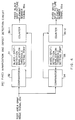
- FIG 4 is the block diagram showing the configuration of the fixed binarization and defect detection circuit 241 forming part of the defect detection binarization circuit 24.
- a comparator 32 compares the test area gray image signal 23a with the value of a black-spot-detection binarization threshold setting port 31 for setting a first black level.
- the comparison result (a picture element of the brightness smaller than the first black level) is provided as a count signal for a counter 36-1.
- the number of fixed black spot picture elements are counted.
- a fixed black spot picture element number signal 35a is output.
- a comparator 34 compares the test area gray image signal 23a with the value of a white-spot-detection binarization threshold setting port 33 for setting a first white level.
- the comparison result (a picture element of the brightness larger than the first white level) is provided as a count signal for a counter 36-2.
- the number of fixed white spot picture elements are counted.
- a fixed white spot picture element number signal 35b is output.
- Figure 5 is the block diagram showing the configuration of the difference binarization and defect detection circuit 242 forming part of the defect detection binarization circuit 24.
- a FIFO memory 41 temporarily stores the test area gray image signal 23a.
- the FIFO memory 41 provides a signal delayed by a predetermined number of picture elements (that is, a background picture element signal) for a subtracter 42.
- the subtracter 42 directly receives the test area gray image signal 23a (that is, an object picture element signal), and subtracts the brightness of the object picture element from the brightness of the background picture element.
- the subtraction result is output to an absolute value conversion circuit 43.
- the absolute value conversion circuit 43 checks a sign bit of the received subtraction result. If it is negative, it is converted into a positive value. Then, a comparator 45 compares the output (difference signal) of the absolute value conversion circuit 43 with the first difference level set by a difference threshold setting port 44. The comparison result (a picture element of the difference larger than the first difference level) is provided as a count signal for a counter 45A. The number of picture elements indicating defective points are counted. Thus, a defective difference picture element number signal 35c is output.
- Figure 6 is the block diagram showing the configuration of the final determination circuit 243 forming the remaining part of the defect detection binarization circuit 24.
- an addition circuit 51 calculates a total of the defect indicating picture element number signals 35a, 35b, and 35c.
- a comparator 52 compares the defect indicating picture element sum area with the first area threshold set in an area threshold setting port 53 for each window area. Thus, the result is output as the Yes/No signal 24a from the comparator 52 to the general determination circuit 15 shown in Figure 3.
- the CPU sets necessary data required to set the first black level, first white level, first difference level, first area threshold, etc. at respective setting points.
- the peak/valley detecting binarization circuit disclosed in Tokugan-hei 3-265134 by the Inventor of the present invention is included in the method of detecting a defective point by the difference binarization shown in Figures 7A and 7B.
- This circuit determines that an object picture element indicates a defective point if two differences obtained by subtracting the value of the object picture element according to the test area gray image signal 23a in a screen scanning line from the values of the background picture elements the equal number of elements (hereinafter referred to as an ⁇ picture elements) before and after the object picture element (hereinafter referred to respectively as a antecedent and subsequent background picture elements) indicate the same polarity, and if one of the two absolute values is larger than a predetermined first threshold of the polarity and the other absolute value is larger than a predetermined second threshold of the polarity.
- the brightness measure circuit 60 shown in Figure 3 is the most important unit of the present invention, and uses a brightness measure area (for example, 150 shown in Figure 7A) stored in the window memory 2 as a gate area.
- Figure 7A shows the circular brightness measure area 150 set in the inner surface of a container.
- the image testing device determines the brightness of a test image. In this case, the brightness of the test image is determined by calculating an average gray level value of some sampled picture elements, not by calculating the gray levels of all picture elements.
- the brightness is measured with sufficient stability by correctly positioning the brightness measure area 150 when the picture elements are extracted such that the coordinate of the center of the brightness measure area 150 matches that of the center of the captured image of the bottom inner surface.
- the binarization threshold which is used in detecting picture elements as black and white spots on a test object, is corrected to vary in proportion to the brightness so as to reduce the precision of a test.
- the image testing device If the measured brightness is monitored and it is smaller than a predetermined threshold more frequently than a predetermined value, the image testing device outputs an alarm to properly maintain the illuminator.
- the brightness measure circuit 60 fetches through the window gate circuit 5E the multivalued gray image signal PO selected by the switching unit 61 or the multivalued gray image signal 1a from the frame memory 1 whichever is included in the gate area. The selected signal is sent to the brightness measure circuit 60 as an input signal to calculate a total of gray level values of picture elements input to the brightness measure circuit 60.
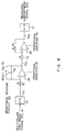
- FIG. 8 shows an example of the brightness measure circuit 60.
- the brightness measure circuit 60 converts the input digital gray image signal (PO or 1a) into an analog signal 71a through a D/A converter 71.
- the analog signal 71a is integrated by an integrator comprising a resistor 72, capacitor 78, operational amplifier 75, and a reset switch 79.
- the output of the integrator (minus signal) 75a is input to an inverter comprising resistors 73 and 74 and an operational amplifier 76 and inverted into a plus signal output 76a.
- the signal 76a is re-converted into a digital signal by an A/D converter 77, and output as the measured brightness signal 60a to the general determination circuit 15 shown in Figure 3.
- the general determination circuit 15 compares the measured brightness signal 60a with an abnormal brightness threshold. If the measured brightness signal 60a is smaller than the abnormal brightness threshold, then a preliminary abnormal brightness counter is incremented by 1. If the measured brightness signal 60a is larger than the abnormal brightness threshold, then a preliminary abnormal brightness counter is cleared to 0. Thus, a preliminary abnormal brightness repetition is obtained. That is, if a preliminary abnormal brightness has arisen, the count value corresponding to the number of determinations can be read from the preliminary abnormal brightness counter.
- the general determination circuit 15 comprises a first abnormal brightness determination unit for comparing the value of the preliminary abnormal brightness counter with the abnormal brightness repetition threshold. If the value of the preliminary abnormal brightness counter is larger than the abnormal brightness repetition threshold, the first abnormal brightness determination unit determines an abnormal brightness.
- the general determination circuit 15 further comprises a second abnormal brightness determination unit for calculating a rate with a predetermined number of determinations made on a test object set as a denominator and a number of determinations causing the preliminary abnormal brightness set as a numerator, for obtaining an average value of the rate variable as the determinations proceeds, and for determining an abnormal brightness when a preliminary abnormal brightness occurrence rate is larger than the threshold preliminarily set in the image testing device.
- the general determination circuit 15 instructs the output circuit 16 shown in Figure 3 to generate an abnormal brightness signal according to the condition of a logical sum of the outputs of abnormal brightness determinations from the first and second abnormal brightness determination units.
- the CPU not shown in the drawings sets necessary data required to set the first black, white, difference, area thresholds, etc. However, in the present invention, these thresholds are corrected by the CPU according to the measured brightness signal 60a as follows.
- the thresholds (hereinafter referred to as an initially-set threshold group) are set when the first black, white, and difference levels (hereinafter referred to generally as a threshold group) are selected for each window area and stored together with the measured brightness (the value of the measured brightness signal 60a, and hereinafter referred to as initially-set brightness).
- the brightness measure circuit 60 obtains a measured brightness (hereinafter referred to as a determined measured brightness) of a test image, and a determined threshold group is calculated and corrected by the CPU not shown in the drawings.
- each abnormal brightness threshold is set under the condition of abnormal brightness threshold #1 > abnormal brightness threshold #2 > abnormal brightness threshold #3 ...
- each abnormal brightness repetition threshold is set under the condition of abnormal brightness repetition threshold #1 > abnormal brightness repetition threshold #2 > abnormal brightness repetition threshold #3 ...
- each abnormal brightness signal #1, #2, #3, ... can be generated under the condition of the logical sum of the first and second abnormal brightness determination units.
- the abnormal brightness signals #1, #2, #3, ... sequentially, and the deterioration level of the light source can be correctly informed. Accordingly, an appropriate maintenance can be provided for the light source.
- a binarization threshold measure area is set in an image of a test object, and an average brightness of the gray level of the image is measured. Then, the binarization threshold, which is used in detecting picture elements as black and white spots on a test object, is corrected to vary in proportion to the brightness so as to reduce the precision of a test.
- the image tester If the measured brightness is monitored and it is smaller than a predetermined threshold more frequently than a predetermined value, the image tester outputs an alarm to properly maintain the illuminator.
Landscapes
- Physics & Mathematics (AREA)
- Health & Medical Sciences (AREA)
- Life Sciences & Earth Sciences (AREA)
- Chemical & Material Sciences (AREA)
- Analytical Chemistry (AREA)
- Biochemistry (AREA)
- General Health & Medical Sciences (AREA)
- General Physics & Mathematics (AREA)
- Immunology (AREA)
- Pathology (AREA)
- Investigating Materials By The Use Of Optical Means Adapted For Particular Applications (AREA)
- Length Measuring Devices By Optical Means (AREA)
- Photometry And Measurement Of Optical Pulse Characteristics (AREA)
- Image Processing (AREA)
- Image Analysis (AREA)
Applications Claiming Priority (3)
| Application Number | Priority Date | Filing Date | Title |
|---|---|---|---|
| JP28541993 | 1993-11-16 | ||
| JP05285419A JP3141654B2 (ja) | 1993-11-16 | 1993-11-16 | 画像検査装置 |
| JP285419/93 | 1993-11-16 |
Publications (3)
| Publication Number | Publication Date |
|---|---|
| EP0660265A2 true EP0660265A2 (fr) | 1995-06-28 |
| EP0660265A3 EP0660265A3 (fr) | 1995-12-27 |
| EP0660265B1 EP0660265B1 (fr) | 2003-02-26 |
Family
ID=17691282
Family Applications (1)
| Application Number | Title | Priority Date | Filing Date |
|---|---|---|---|
| EP94118021A Expired - Lifetime EP0660265B1 (fr) | 1993-11-16 | 1994-11-15 | Appareil de test d'une image d'un objet à tester |
Country Status (4)
| Country | Link |
|---|---|
| US (1) | US5608815A (fr) |
| EP (1) | EP0660265B1 (fr) |
| JP (1) | JP3141654B2 (fr) |
| DE (1) | DE69432169T2 (fr) |
Cited By (1)
| Publication number | Priority date | Publication date | Assignee | Title |
|---|---|---|---|---|
| GB2398690A (en) * | 2003-02-21 | 2004-08-25 | Sony Comp Entertainment Europe | Control of an image processor in dependance of image luminance |
Families Citing this family (9)
| Publication number | Priority date | Publication date | Assignee | Title |
|---|---|---|---|---|
| JP3216767B2 (ja) | 1995-02-28 | 2001-10-09 | 富士電機株式会社 | レベル変動補正可能な画像処理装置 |
| JPH10209210A (ja) | 1997-01-20 | 1998-08-07 | Sharp Corp | 半導体装置及びその製造方法並びにその検査方法 |
| JP2000260815A (ja) | 1999-03-10 | 2000-09-22 | Mitsubishi Electric Corp | バンプの溶融方法および溶融装置、ならびに半導体装置の製造方法 |
| JP4649828B2 (ja) * | 2003-10-17 | 2011-03-16 | Jfeスチール株式会社 | 画像処理装置の異常の判定方法 |
| US8135206B2 (en) * | 2007-05-02 | 2012-03-13 | Emhart Glass S.A. | Machine for inspecting glass containers |
| JP4918003B2 (ja) * | 2007-09-11 | 2012-04-18 | 株式会社日立情報制御ソリューションズ | 診断装置、診断方法、および検査装置 |
| JP5075893B2 (ja) * | 2009-09-15 | 2012-11-21 | 株式会社東芝 | パターン検査システム |
| CN113255657B (zh) * | 2020-12-31 | 2024-04-05 | 深圳怡化电脑股份有限公司 | 票据表面刮痕检测方法、装置、电子设备、机器可读介质 |
| CN115457444B (zh) * | 2022-09-21 | 2026-01-02 | 上海施成照明工程有限公司 | 灯具故障自动化识别的方法、系统、电子设备及存储介质 |
Family Cites Families (6)
| Publication number | Priority date | Publication date | Assignee | Title |
|---|---|---|---|---|
| US4827351A (en) * | 1985-08-14 | 1989-05-02 | Canon Kabushiki Kaisha | Image reading apparatus with controlled correction for unevenness in illumination |
| JP2834234B2 (ja) * | 1989-02-14 | 1998-12-09 | シチズン時計株式会社 | カレンダ表示装置 |
| JPH03205540A (ja) * | 1990-01-08 | 1991-09-09 | Kubota Corp | 欠陥検出方法 |
| US5268773A (en) * | 1990-03-30 | 1993-12-07 | Samsung Electronics Co., Ltd. | Document image signal processor having an adaptive threshold |
| JPH0736001B2 (ja) * | 1990-10-31 | 1995-04-19 | 東洋ガラス株式会社 | びんの欠陥検査方法 |
| US5233199A (en) * | 1991-07-15 | 1993-08-03 | Fuji Electric Co., Ltd. | Cylindrical container's inner surface tester |
-
1993
- 1993-11-16 JP JP05285419A patent/JP3141654B2/ja not_active Expired - Lifetime
-
1994
- 1994-11-15 US US08/339,957 patent/US5608815A/en not_active Expired - Fee Related
- 1994-11-15 EP EP94118021A patent/EP0660265B1/fr not_active Expired - Lifetime
- 1994-11-15 DE DE69432169T patent/DE69432169T2/de not_active Expired - Fee Related
Cited By (3)
| Publication number | Priority date | Publication date | Assignee | Title |
|---|---|---|---|---|
| GB2398690A (en) * | 2003-02-21 | 2004-08-25 | Sony Comp Entertainment Europe | Control of an image processor in dependance of image luminance |
| GB2398690B (en) * | 2003-02-21 | 2006-05-10 | Sony Comp Entertainment Europe | Control of data processing |
| US8035613B2 (en) | 2003-02-21 | 2011-10-11 | Sony Computer Entertainment Europe Ltd. | Control of data processing |
Also Published As
| Publication number | Publication date |
|---|---|
| JP3141654B2 (ja) | 2001-03-05 |
| US5608815A (en) | 1997-03-04 |
| DE69432169D1 (de) | 2003-04-03 |
| EP0660265B1 (fr) | 2003-02-26 |
| EP0660265A3 (fr) | 1995-12-27 |
| JPH07140092A (ja) | 1995-06-02 |
| DE69432169T2 (de) | 2003-11-20 |
Similar Documents
| Publication | Publication Date | Title |
|---|---|---|
| EP0595261B1 (fr) | Méthode pour l'inspection de la présence de matières étrangères dans un corps solide | |
| US5608815A (en) | Device for testing an image of a test object | |
| GB2435325A (en) | Automatic judging device and automatic judging method | |
| US6912303B2 (en) | Method for testing the reliability of a testing apparatus, especially an empty bottle inspector | |
| US5233199A (en) | Cylindrical container's inner surface tester | |
| JP4253527B2 (ja) | 自動判別装置 | |
| CN111665249A (zh) | 一种光强调整方法、系统及光学检测设备 | |
| EP0610956A2 (fr) | Dispositif pour contrôler la surface intérieure d'un récipient | |
| JP4649828B2 (ja) | 画像処理装置の異常の判定方法 | |
| EP0540018A2 (fr) | Dispositif pour contrôler la surface intérieure d'un récipient cylindrique, utilisant une technique de traitement d'image | |
| US6963076B1 (en) | System and method for optically sensing defects in OPC devices | |
| EP0599335A2 (fr) | Dispositif de contrôle de la surface interne d'un récipient cylindrique | |
| JP3055323B2 (ja) | 円形容器内面検査装置 | |
| KR100484675B1 (ko) | 플라즈마 디스플레이 패널 검사 시스템 및 이를 이용한검사 방법 | |
| JP2004084498A (ja) | エンジン評価装置及び方法 | |
| JPH06109432A (ja) | 寸法測定装置 | |
| KR100289442B1 (ko) | 화상디바이스 검사를 위한 먼지 구별 장치 및 그 방법 | |
| JPH10153558A (ja) | 検査装置 | |
| JPH0572141A (ja) | 円形容器内面検査装置 | |
| KR200201713Y1 (ko) | 브라운관 펀넬용 애노드 단자부의 양부 검사 장치 및 이를 이용한 검사방법 | |
| JPH07159141A (ja) | ワーク表面検査方法 | |
| CN121402321A (zh) | 陶瓷过滤片缺陷检测方法、装置、设备及存储介质 | |
| JPH0518909A (ja) | 円形容器内面検査装置 | |
| JPH0587738A (ja) | 円形容器内面検査装置 | |
| JPH03226875A (ja) | 画像処理装置 |
Legal Events
| Date | Code | Title | Description |
|---|---|---|---|
| PUAI | Public reference made under article 153(3) epc to a published international application that has entered the european phase |
Free format text: ORIGINAL CODE: 0009012 |
|
| AK | Designated contracting states |
Kind code of ref document: A2 Designated state(s): DE FR GB |
|
| PUAL | Search report despatched |
Free format text: ORIGINAL CODE: 0009013 |
|
| AK | Designated contracting states |
Kind code of ref document: A3 Designated state(s): DE FR GB |
|
| 17P | Request for examination filed |
Effective date: 19960411 |
|
| 17Q | First examination report despatched |
Effective date: 19990907 |
|
| GRAG | Despatch of communication of intention to grant |
Free format text: ORIGINAL CODE: EPIDOS AGRA |
|
| GRAG | Despatch of communication of intention to grant |
Free format text: ORIGINAL CODE: EPIDOS AGRA |
|
| GRAH | Despatch of communication of intention to grant a patent |
Free format text: ORIGINAL CODE: EPIDOS IGRA |
|
| GRAH | Despatch of communication of intention to grant a patent |
Free format text: ORIGINAL CODE: EPIDOS IGRA |
|
| GRAA | (expected) grant |
Free format text: ORIGINAL CODE: 0009210 |
|
| AK | Designated contracting states |
Designated state(s): DE FR GB |
|
| REG | Reference to a national code |
Ref country code: GB Ref legal event code: FG4D |
|
| REF | Corresponds to: |
Ref document number: 69432169 Country of ref document: DE Date of ref document: 20030403 Kind code of ref document: P |
|
| ET | Fr: translation filed | ||
| PGFP | Annual fee paid to national office [announced via postgrant information from national office to epo] |
Ref country code: FR Payment date: 20031110 Year of fee payment: 10 |
|
| PGFP | Annual fee paid to national office [announced via postgrant information from national office to epo] |
Ref country code: GB Payment date: 20031112 Year of fee payment: 10 |
|
| PGFP | Annual fee paid to national office [announced via postgrant information from national office to epo] |
Ref country code: DE Payment date: 20031127 Year of fee payment: 10 |
|
| PLBE | No opposition filed within time limit |
Free format text: ORIGINAL CODE: 0009261 |
|
| STAA | Information on the status of an ep patent application or granted ep patent |
Free format text: STATUS: NO OPPOSITION FILED WITHIN TIME LIMIT |
|
| 26N | No opposition filed |
Effective date: 20031127 |
|
| PG25 | Lapsed in a contracting state [announced via postgrant information from national office to epo] |
Ref country code: GB Free format text: LAPSE BECAUSE OF NON-PAYMENT OF DUE FEES Effective date: 20041115 |
|
| PG25 | Lapsed in a contracting state [announced via postgrant information from national office to epo] |
Ref country code: DE Free format text: LAPSE BECAUSE OF NON-PAYMENT OF DUE FEES Effective date: 20050601 |
|
| GBPC | Gb: european patent ceased through non-payment of renewal fee |
Effective date: 20041115 |
|
| PG25 | Lapsed in a contracting state [announced via postgrant information from national office to epo] |
Ref country code: FR Free format text: LAPSE BECAUSE OF NON-PAYMENT OF DUE FEES Effective date: 20050729 |
|
| REG | Reference to a national code |
Ref country code: FR Ref legal event code: ST |