EP0660389A2 - Procédé pour fabriquer des dispositifs semi-conducteurs comportant des régions de séparation - Google Patents
Procédé pour fabriquer des dispositifs semi-conducteurs comportant des régions de séparation Download PDFInfo
- Publication number
- EP0660389A2 EP0660389A2 EP94120685A EP94120685A EP0660389A2 EP 0660389 A2 EP0660389 A2 EP 0660389A2 EP 94120685 A EP94120685 A EP 94120685A EP 94120685 A EP94120685 A EP 94120685A EP 0660389 A2 EP0660389 A2 EP 0660389A2
- Authority
- EP
- European Patent Office
- Prior art keywords
- material layer
- film
- substrate
- layer
- element separating
- Prior art date
- Legal status (The legal status is an assumption and is not a legal conclusion. Google has not performed a legal analysis and makes no representation as to the accuracy of the status listed.)
- Granted
Links
Images


Classifications
-
- H—ELECTRICITY
- H10—SEMICONDUCTOR DEVICES; ELECTRIC SOLID-STATE DEVICES NOT OTHERWISE PROVIDED FOR
- H10P—GENERIC PROCESSES OR APPARATUS FOR THE MANUFACTURE OR TREATMENT OF DEVICES COVERED BY CLASS H10
- H10P50/00—Etching of wafers, substrates or parts of devices
- H10P50/69—Etching of wafers, substrates or parts of devices using masks for semiconductor materials
- H10P50/691—Etching of wafers, substrates or parts of devices using masks for semiconductor materials for Group V materials or Group III-V materials
- H10P50/692—Etching of wafers, substrates or parts of devices using masks for semiconductor materials for Group V materials or Group III-V materials characterised by their composition, e.g. multilayer masks or materials
-
- H—ELECTRICITY
- H10—SEMICONDUCTOR DEVICES; ELECTRIC SOLID-STATE DEVICES NOT OTHERWISE PROVIDED FOR
- H10W—GENERIC PACKAGES, INTERCONNECTIONS, CONNECTORS OR OTHER CONSTRUCTIONAL DETAILS OF DEVICES COVERED BY CLASS H10
- H10W10/00—Isolation regions in semiconductor bodies between components of integrated devices
- H10W10/01—Manufacture or treatment
- H10W10/011—Manufacture or treatment of isolation regions comprising dielectric materials
- H10W10/014—Manufacture or treatment of isolation regions comprising dielectric materials using trench refilling with dielectric materials, e.g. shallow trench isolations
-
- H—ELECTRICITY
- H10—SEMICONDUCTOR DEVICES; ELECTRIC SOLID-STATE DEVICES NOT OTHERWISE PROVIDED FOR
- H10W—GENERIC PACKAGES, INTERCONNECTIONS, CONNECTORS OR OTHER CONSTRUCTIONAL DETAILS OF DEVICES COVERED BY CLASS H10
- H10W10/00—Isolation regions in semiconductor bodies between components of integrated devices
- H10W10/10—Isolation regions comprising dielectric materials
- H10W10/17—Isolation regions comprising dielectric materials formed using trench refilling with dielectric materials, e.g. shallow trench isolations
Definitions
- the present invention relates to a method of manufacturing semiconductor devices, and more specifically to a method of manufacturing semiconductor devices having buried element separating regions.
- Figs. 3(A) to 3(D) are cross-sectional views for assistance in explaining the conventional method of manufacturing the buried element separating region, in particular.
- a SiO2 film 2 with a thickness of about 10 nm, for instance is formed on a Si substrate by thermal oxidization.
- a resist film 5 is applied onto the SiO2 film 2, and further the resist film 5 is formed into a predetermined shape in accordance with photolithography. Further, by using the formed resist film 5 as a mask, an element separating trench 7 with a depth of about 500 nm, for instance is formed in the SiO2 film 2 and the Si substrate by anisotropic etching.
- another SiO2 film 8 with a thickness of a bout 20 nm, for instance is deposited thereon by thermal oxidization.
- another SiO2 9 film with a thickness of about 1 ⁇ m, for instance is further deposited thereon as a trench filling substance.
- the deposited filling substance of the SiO2 film 9 is etched back by anisotropic etching or polishing to complete the buried element separating region 10.
- a gate oxide film 11 with a thickness of about 10 nm is formed thereon by thermal oxidization.
- a poly crystalline Si film 12 with a thickness of about 300 nm, for instance is formed into a predetermined shape as a gate electrode.
- kink characteristics occur because the characteristics of a parasitic transistor are added to the original I-V characteristics of the MOSFET.
- edge portion 13 is a corner of the Si substrate as shown in Fig. 3(D)
- a mechanical stress tends to be concentrated and thereby a defect tends to occurs easily at the edge portion 13, thus causing a problem in that a leakage tends to occur in the gate oxide film 11.
- the present invention provides a method of manufacturing a semiconductor device, comprising the steps of: forming a first material layer (3) and a second material layer (5) in sequence on a surface of a semiconductor substrate (1); forming a first opening on the first material layer (3) and a second opening in the second material layer (5), the first opening being larger than the second opening; forming an element separating trench (7) under the second opening in the substrate (1) by using the second material layer (5) as a mask; removing the second material layer (5); depositing a filling material (9) on the element separating trench (7), the substrate (1) and the first material layer (3); and etching back the filling material (9) by using the first material layer (3) as a stopper.
- the present invention provides a method of manufacturing a semiconductor device, comprising the steps of: forming a first material layer (3), a second material layer (4), and a third material layer (5) on a surface of a semiconductor substrate (1); patterning the third material layer (5); etching the second and the first material layers (4, 3) by using the third material layer (5) as a mask to form a first opening on the first material layer (3) and a second opening in the second material layer (4), the first opening being larger than the second opening; forming an element separating trench (7) under the second opening in the substrate (1) by using the second material layer (4) as a mask; removing the second material layer (4); depositing a filling material (9) on the element separating trench (7), the substrate (1) and the first material layer (3); and etching back the filling material (9) by using the first material layer (3) as a stopper.
- the first opening of the first layer deposited on the semiconductor substrate is determined to be broader than the opening of the element separating trench formed on the semiconductor substrate, it is possible to cover the edge portion (formed between the substrate surface and the element separating trench) with a filling substance deposited in the trench and on the surface of the semiconductor substrate. As a result, it is possible to eliminate defects which may cause the electric field concentration and the gate oxide film leakage at the edge portion.
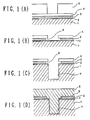
- Fig. 1(A) to (G) show a first embodiment of the manufacturing method according to the present invention.
- a SiO2 film 2 with a thickness of about 10 nm, for instance is formed on a Si substrate 1 by thermal oxidization. Then, a poly crystalline Si film 3 with a thickness of about 200 nm, for instance is deposited by chemical vapor deposition method. Further, a SiO2 film 4 with a thickness of about 200 nm, for instance is deposited thereon by chemical vapor deposition method. After that, a resist film 5 is applied onto the SiO2 film 4, and then the resist film 5 is formed into a predetermined shape in accordance with photolithography.
- the SiO2 film 4 and the poly crystalline Si film 3 are both process by anisotropic etching in sequence to remove the resist film 5.
- the poly crystalline Si film 3 is etched back by isotropic etching to form a recessed portion 6 with a recession of about 100 nm, for instance.
- CDE method chemical dry etching
- wet processing, etc. are known. In any method, however, it is possible to form the recessed portion 6 as shown in Fig. 1(B).
- the SiO2 film 2 is removed, and further the Si substrate 1 is etched to form an element separating trench 7 with a depth of about 500 nm (so that a buried element separating region can be formed later).
- the SiO2 film 4 used as a mask for etching the Si substrate 1 is also etched simultaneously, since the film thickness (10 nm) of the SiO2 film 2 is sufficiently thinner than that (200 nm) of the SiO2 film 4 (used as an etching mask), the thickness of the SiO2 film 4 can be almost maintained.
- a SiO2 film 8 with a thickness of about 20 nm is formed by thermal oxidization in order to remove defects produced on the Si substrate 1 when the Si substrate 1 is etched.
- SiO2 film 9 with a thickness of about 1 ⁇ m, for instance is further deposited thereon by chemical vapor deposition method as a filling substance of the element separating trench 7 (as a buried element separation).
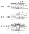
- the deposited filling substance of SiO2 film 9 is etched back by anisotropic etching or polishing by use of the poly crystalline Si film 3 as a stopper film, the etching of the filling substance SiO2 film 9 can be stopped at a level flush with the poly crystalline Si film 3 to form the buried element separating region 10.
- the poly crystalline Si film 3 used as a stopper during the etching back is removed to complete the buried element separating region 10.
- a poly crystalline Si film 12 is deposited all over the device to complete a semiconductor device.
- the buried element separating region 10 formed in accordance with the above-mentioned method is of concave shape.
- the edge portion 13 of the Si substrate 1 is covered with the SiO2 film 9 for filling the buried element separating trench 7, it is possible to eliminate electric field concentration and defects at the corner thereof, so that it is possible to realize an LSI of high reliability.
- the SiO2 film 4 is used as a mask for etching the Si substrate 1 to form the element separating trench 7, and the poly crystalline Si film 3 is used as an etching stopper film when the filling substance of the buried element separating region 10 is etched back.
- the etching mask used when the Si substrate 1 is etched to form the element separating trench 7
- the etching stopper used when the filling substance is etched back
- a WSi film, TiN film, carbon film, SiN film, etc are usable as the etching stopper.
- the SiO2 is used as the substance for filling the buried element separating trench 7.
- other filling substances such as Si, SiN, etc.
- SiO2 film and SiN film can be used as the poly crystalline Si film 3 and the SiO2 film 4, both shown in Fig. 1(A), or vice versa.
- the poly crystalline Si film 3 and the SiO2 film 4 are deposited in sequence; these films 3 and 4 are etched by use of a resist film 5 formed into a predetermined shape as a mask; and the SiO2 film 4 is used as a mask to etch the element separating trench 7.
- a resist film 5 formed into a predetermined shape as a mask
- the SiO2 film 4 is used as a mask to etch the element separating trench 7.
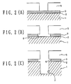
- Fig. 2(A) to (C) show a second embodiment of the manufacturing method according to the present invention, which is described from the above-mentioned point of view..
- a SiO2 film 2 with a thickness of about 10 nm, for instance is formed on a Si substrate 1 by thermal oxidization.
- a poly crystalline Si film 3 with a thickness of about 200 nm, for instance is deposited by chemical vapor deposition method.
- a resist film 5 is applied thereonto and formed into a predetermined shape in accordance with photolithography.
- the poly crystalline Si film 3 is processed by anisotropic etching, and further etched by isotropic etching to form a recessed portion 6 with a recess of about 100 nm.
- CDE method chemical dry etching
- wet processing etc.
- the SiO2 film 2 is removed to expose the surface of the Si substrate 1, and the exposed Si substrate 1 is etched to a depth of about 500 nm (sufficient depth as the buried element separation) by use of the SiO2 film 2 as a mask to form an element separating trench 7.
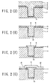
- ions are implanted to control the threshold level to a predetermined value; after the SiO2 film 2 and the SiO2 film 8 above the surface of the Si substrate 1 has been removed, a gate oxide film 11 with a thickness of about 10 nm is formed by thermal oxidization; and after that, a poly crystalline Si film 12 with a thickness of about 300 nm, for instance is deposited and formed into a predetermined shape as a gate electrode.
- Fig. 1(G) the device thus obtained is shown in Fig. 1(G).
- Si nitride film instead of the SiO2 films 2, 4 and 8. Further, it is also possible to use both the SiO2 film and Si nitride film in combination.
- the SiO2 film 2 can be replaced with a carbon film, TiN film, or siliside metal, etc.
- the SiO2 film 4 can be replaced with Si oxide film, Si nitride film, Si film, or resist film, etc.
- the SiO2 film 8 can be replaced with Si oxide film, Si nitride film, or Si film.
- the semiconductor device As described above, in the method of manufacturing the semiconductor device according to the present invention, after materials are deposited in sequence on the substrate, a part of the material is recessed in the horizontal direction along the surface of the substrate to form a recessed portion; after that, an element separating trench is formed; another material is deposited; and the whole device is etched back. Therefore, since a convex buried element separating region 10 can be formed and in addition since the edge portion of the substrate can be covered with the element separating region filling material, it is possible to prevent the electric field from being concentrated at the corner portion of the substrate and to prevent a defect from occurring at the corner portion of the substrate, thus providing miniaturized semiconductor device of higher reliability.
- the edge portion of the element separating trench formed in the semiconductor substrate can be covered with the trench filling material, it is possible to provide a semiconductor device which can suppress electric field concentration at the edge portion of the substrate and thereby to prevent the defect from being produced at the edge portion thereof.
Landscapes
- Element Separation (AREA)
Applications Claiming Priority (3)
| Application Number | Priority Date | Filing Date | Title |
|---|---|---|---|
| JP33319593 | 1993-12-27 | ||
| JP5333195A JPH07193121A (ja) | 1993-12-27 | 1993-12-27 | 半導体装置の製造方法 |
| JP333195/93 | 1993-12-27 |
Publications (3)
| Publication Number | Publication Date |
|---|---|
| EP0660389A2 true EP0660389A2 (fr) | 1995-06-28 |
| EP0660389A3 EP0660389A3 (fr) | 1997-12-29 |
| EP0660389B1 EP0660389B1 (fr) | 2002-02-27 |
Family
ID=18263378
Family Applications (1)
| Application Number | Title | Priority Date | Filing Date |
|---|---|---|---|
| EP94120685A Expired - Lifetime EP0660389B1 (fr) | 1993-12-27 | 1994-12-27 | Procédé pour fabriquer des dispositifs semi-conducteurs comportant des régions de séparation |
Country Status (5)
| Country | Link |
|---|---|
| US (1) | US5766823A (fr) |
| EP (1) | EP0660389B1 (fr) |
| JP (1) | JPH07193121A (fr) |
| KR (1) | KR0179681B1 (fr) |
| DE (1) | DE69429978T2 (fr) |
Cited By (2)
| Publication number | Priority date | Publication date | Assignee | Title |
|---|---|---|---|---|
| FR2792113A1 (fr) * | 1999-04-06 | 2000-10-13 | St Microelectronics Sa | Procede de realisation d'un circuit integre comportant une tranchee d'isolation laterale accolee a une zone active d'un transistor, et circuit integre correspondant |
| US6265743B1 (en) | 1997-04-11 | 2001-07-24 | Mitsubishi Denki Kabushiki Kaisha | Trench type element isolation structure |
Families Citing this family (23)
| Publication number | Priority date | Publication date | Assignee | Title |
|---|---|---|---|---|
| JP3688816B2 (ja) * | 1996-07-16 | 2005-08-31 | 株式会社東芝 | 半導体装置の製造方法 |
| US6114741A (en) * | 1996-12-13 | 2000-09-05 | Texas Instruments Incorporated | Trench isolation of a CMOS structure |
| KR19980051524A (ko) * | 1996-12-23 | 1998-09-15 | 김영환 | 반도체소자의 소자분리막 제조방법 |
| KR19980060506A (ko) * | 1996-12-31 | 1998-10-07 | 김영환 | 반도체 소자의 소자 분리막 형성방법 |
| JP3614267B2 (ja) * | 1997-02-05 | 2005-01-26 | 株式会社ルネサステクノロジ | 半導体集積回路装置の製造方法 |
| JPH10223747A (ja) * | 1997-02-06 | 1998-08-21 | Nec Corp | 半導体装置の製造方法 |
| US5960297A (en) * | 1997-07-02 | 1999-09-28 | Kabushiki Kaisha Toshiba | Shallow trench isolation structure and method of forming the same |
| US5981356A (en) * | 1997-07-28 | 1999-11-09 | Integrated Device Technology, Inc. | Isolation trenches with protected corners |
| US5837612A (en) * | 1997-08-01 | 1998-11-17 | Motorola, Inc. | Silicon chemical mechanical polish etch (CMP) stop for reduced trench fill erosion and method for formation |
| US6103635A (en) * | 1997-10-28 | 2000-08-15 | Fairchild Semiconductor Corp. | Trench forming process and integrated circuit device including a trench |
| US6054343A (en) * | 1998-01-26 | 2000-04-25 | Texas Instruments Incorporated | Nitride trench fill process for increasing shallow trench isolation (STI) robustness |
| US5976948A (en) * | 1998-02-19 | 1999-11-02 | Advanced Micro Devices | Process for forming an isolation region with trench cap |
| US6214699B1 (en) * | 1998-04-01 | 2001-04-10 | Texas Instruments Incorporated | Method for forming an isolation structure in a substrate |
| KR19990079343A (ko) * | 1998-04-03 | 1999-11-05 | 윤종용 | 반도체장치의 트렌치 소자분리 방법 |
| US6265282B1 (en) | 1998-08-17 | 2001-07-24 | Micron Technology, Inc. | Process for making an isolation structure |
| JP3540633B2 (ja) * | 1998-11-11 | 2004-07-07 | 株式会社東芝 | 半導体装置の製造方法 |
| KR20000066999A (ko) * | 1999-04-22 | 2000-11-15 | 김영환 | 반도체 장치의 분리구조 제조방법 |
| JP2001118920A (ja) * | 1999-10-15 | 2001-04-27 | Seiko Epson Corp | 半導体装置およびその製造方法 |
| US6406982B2 (en) * | 2000-06-05 | 2002-06-18 | Denso Corporation | Method of improving epitaxially-filled trench by smoothing trench prior to filling |
| JP2002203894A (ja) * | 2001-01-04 | 2002-07-19 | Mitsubishi Electric Corp | 半導体装置の製造方法 |
| KR100546852B1 (ko) * | 2002-12-28 | 2006-01-25 | 동부아남반도체 주식회사 | 반도체 소자의 제조 방법 |
| US7119403B2 (en) * | 2003-10-16 | 2006-10-10 | International Business Machines Corporation | High performance strained CMOS devices |
| US6905943B2 (en) * | 2003-11-06 | 2005-06-14 | Texas Instruments Incorporated | Forming a trench to define one or more isolation regions in a semiconductor structure |
Family Cites Families (7)
| Publication number | Priority date | Publication date | Assignee | Title |
|---|---|---|---|---|
| EP0048175B1 (fr) * | 1980-09-17 | 1986-04-23 | Hitachi, Ltd. | Dispositif semi-conducteur et procédé pour sa fabrication |
| CA1204525A (fr) * | 1982-11-29 | 1986-05-13 | Tetsu Fukano | Methode d'isolation zonee sur elements electriques |
| US4666556A (en) * | 1986-05-12 | 1987-05-19 | International Business Machines Corporation | Trench sidewall isolation by polysilicon oxidation |
| JP2666384B2 (ja) * | 1988-06-30 | 1997-10-22 | ソニー株式会社 | 半導体装置の製造方法 |
| US5290664A (en) * | 1990-03-29 | 1994-03-01 | Sharp Kabushiki Kaisha | Method for preparing electrode for semiconductor device |
| US5413966A (en) * | 1990-12-20 | 1995-05-09 | Lsi Logic Corporation | Shallow trench etch |
| JPH0629239A (ja) * | 1992-02-27 | 1994-02-04 | Eastman Kodak Co | リフト−オフプロセスを利用した半導体素子におけるセルフアライン拡散バリアの製造方法及び拡散バリアを有する半導体素子 |
-
1993
- 1993-12-27 JP JP5333195A patent/JPH07193121A/ja active Pending
-
1994
- 1994-12-26 KR KR1019940036760A patent/KR0179681B1/ko not_active Expired - Fee Related
- 1994-12-27 EP EP94120685A patent/EP0660389B1/fr not_active Expired - Lifetime
- 1994-12-27 DE DE69429978T patent/DE69429978T2/de not_active Expired - Lifetime
-
1997
- 1997-09-22 US US08/935,058 patent/US5766823A/en not_active Expired - Lifetime
Cited By (3)
| Publication number | Priority date | Publication date | Assignee | Title |
|---|---|---|---|---|
| US6265743B1 (en) | 1997-04-11 | 2001-07-24 | Mitsubishi Denki Kabushiki Kaisha | Trench type element isolation structure |
| US6372604B1 (en) | 1997-04-11 | 2002-04-16 | Mitsubishi Denki Kabushiki Kaisha | Method for forming a trench type element isolation structure and trench type element isolation structure |
| FR2792113A1 (fr) * | 1999-04-06 | 2000-10-13 | St Microelectronics Sa | Procede de realisation d'un circuit integre comportant une tranchee d'isolation laterale accolee a une zone active d'un transistor, et circuit integre correspondant |
Also Published As
| Publication number | Publication date |
|---|---|
| EP0660389B1 (fr) | 2002-02-27 |
| KR0179681B1 (ko) | 1999-04-15 |
| DE69429978D1 (de) | 2002-04-04 |
| DE69429978T2 (de) | 2002-10-02 |
| EP0660389A3 (fr) | 1997-12-29 |
| US5766823A (en) | 1998-06-16 |
| JPH07193121A (ja) | 1995-07-28 |
Similar Documents
| Publication | Publication Date | Title |
|---|---|---|
| US5766823A (en) | Method of manufacturing semiconductor devices | |
| US5677229A (en) | Method for manufacturing semiconductor device isolation region | |
| US8338264B2 (en) | Methods for forming isolation structures for semiconductor devices | |
| US5843839A (en) | Formation of a metal via using a raised metal plug structure | |
| US6482718B2 (en) | Method of manufacturing semiconductor device | |
| US5976948A (en) | Process for forming an isolation region with trench cap | |
| US5882981A (en) | Mesa isolation Refill Process for Silicon on Insulator Technology Using Flowage Oxides as the Refill Material | |
| KR100307651B1 (ko) | 반도체장치의제조방법 | |
| JP2001196576A (ja) | 半導体装置およびその製造方法 | |
| JP2003243293A (ja) | 半導体装置の製造方法 | |
| US6664162B2 (en) | Method of manufacturing capacitor | |
| JP2757919B2 (ja) | 半導体装置の製造方法 | |
| KR100308198B1 (ko) | 에스오아이 반도체 소자 분리 방법 | |
| KR100278883B1 (ko) | 반도체 소자 분리를 위한 얕은 트렌치 제조 방법 | |
| JPH10242264A (ja) | 半導体装置の製造方法 | |
| US6025272A (en) | Method of planarize and improve the effectiveness of the stop layer | |
| JPH11251318A (ja) | 半導体装置及びその製造方法 | |
| KR0161727B1 (ko) | 반도체 소자의 소자분리방법 | |
| US6833295B2 (en) | Method of manufacturing a semiconductor device | |
| JPS63257244A (ja) | 半導体装置およびその製造方法 | |
| JPH07135308A (ja) | 半導体装置の製造方法 | |
| JP3609660B2 (ja) | 半導体装置の製造方法及び半導体装置 | |
| KR100367741B1 (ko) | 개선된 보더리스 콘택 구조 및 그 제조방법 | |
| KR100223825B1 (ko) | 반도체 소자의 격리영역 형성방법 | |
| KR100565749B1 (ko) | 반도체 소자의 격리영역 및 그 제조방법 |
Legal Events
| Date | Code | Title | Description |
|---|---|---|---|
| PUAI | Public reference made under article 153(3) epc to a published international application that has entered the european phase |
Free format text: ORIGINAL CODE: 0009012 |
|
| 17P | Request for examination filed |
Effective date: 19941227 |
|
| AK | Designated contracting states |
Kind code of ref document: A2 Designated state(s): DE FR GB |
|
| PUAL | Search report despatched |
Free format text: ORIGINAL CODE: 0009013 |
|
| AK | Designated contracting states |
Kind code of ref document: A3 Designated state(s): DE FR GB |
|
| 17Q | First examination report despatched |
Effective date: 19991125 |
|
| GRAG | Despatch of communication of intention to grant |
Free format text: ORIGINAL CODE: EPIDOS AGRA |
|
| GRAG | Despatch of communication of intention to grant |
Free format text: ORIGINAL CODE: EPIDOS AGRA |
|
| GRAH | Despatch of communication of intention to grant a patent |
Free format text: ORIGINAL CODE: EPIDOS IGRA |
|
| GRAH | Despatch of communication of intention to grant a patent |
Free format text: ORIGINAL CODE: EPIDOS IGRA |
|
| REG | Reference to a national code |
Ref country code: GB Ref legal event code: IF02 |
|
| GRAA | (expected) grant |
Free format text: ORIGINAL CODE: 0009210 |
|
| AK | Designated contracting states |
Kind code of ref document: B1 Designated state(s): DE FR GB |
|
| REF | Corresponds to: |
Ref document number: 69429978 Country of ref document: DE Date of ref document: 20020404 |
|
| ET | Fr: translation filed | ||
| PLBE | No opposition filed within time limit |
Free format text: ORIGINAL CODE: 0009261 |
|
| STAA | Information on the status of an ep patent application or granted ep patent |
Free format text: STATUS: NO OPPOSITION FILED WITHIN TIME LIMIT |
|
| 26N | No opposition filed |
Effective date: 20021128 |
|
| PGFP | Annual fee paid to national office [announced via postgrant information from national office to epo] |
Ref country code: FR Payment date: 20101224 Year of fee payment: 17 |
|
| PGFP | Annual fee paid to national office [announced via postgrant information from national office to epo] |
Ref country code: GB Payment date: 20101222 Year of fee payment: 17 |
|
| PGFP | Annual fee paid to national office [announced via postgrant information from national office to epo] |
Ref country code: DE Payment date: 20101222 Year of fee payment: 17 |
|
| GBPC | Gb: european patent ceased through non-payment of renewal fee |
Effective date: 20111227 |
|
| REG | Reference to a national code |
Ref country code: FR Ref legal event code: ST Effective date: 20120831 |
|
| REG | Reference to a national code |
Ref country code: DE Ref legal event code: R119 Ref document number: 69429978 Country of ref document: DE Effective date: 20120703 |
|
| PG25 | Lapsed in a contracting state [announced via postgrant information from national office to epo] |
Ref country code: GB Free format text: LAPSE BECAUSE OF NON-PAYMENT OF DUE FEES Effective date: 20111227 Ref country code: DE Free format text: LAPSE BECAUSE OF NON-PAYMENT OF DUE FEES Effective date: 20120703 |
|
| PG25 | Lapsed in a contracting state [announced via postgrant information from national office to epo] |
Ref country code: FR Free format text: LAPSE BECAUSE OF NON-PAYMENT OF DUE FEES Effective date: 20120102 |