EP0660651A1 - Substrat céramique à circuit multicouche, procédé de production, et matériau électriquement conducteur pour utilisation dans un substrat céramique à circuit multicouche - Google Patents
Substrat céramique à circuit multicouche, procédé de production, et matériau électriquement conducteur pour utilisation dans un substrat céramique à circuit multicouche Download PDFInfo
- Publication number
- EP0660651A1 EP0660651A1 EP94120404A EP94120404A EP0660651A1 EP 0660651 A1 EP0660651 A1 EP 0660651A1 EP 94120404 A EP94120404 A EP 94120404A EP 94120404 A EP94120404 A EP 94120404A EP 0660651 A1 EP0660651 A1 EP 0660651A1
- Authority
- EP
- European Patent Office
- Prior art keywords
- powder
- circuit substrate
- multilayer ceramic
- ceramic circuit
- conductor patterns
- Prior art date
- Legal status (The legal status is an assumption and is not a legal conclusion. Google has not performed a legal analysis and makes no representation as to the accuracy of the status listed.)
- Granted
Links
Images
Classifications
-
- H—ELECTRICITY
- H05—ELECTRIC TECHNIQUES NOT OTHERWISE PROVIDED FOR
- H05K—PRINTED CIRCUITS; CASINGS OR CONSTRUCTIONAL DETAILS OF ELECTRIC APPARATUS; MANUFACTURE OF ASSEMBLAGES OF ELECTRICAL COMPONENTS
- H05K3/00—Apparatus or processes for manufacturing printed circuits
- H05K3/22—Secondary treatment of printed circuits
- H05K3/24—Reinforcing of the conductive pattern
- H05K3/245—Reinforcing conductive patterns made by printing techniques or by other techniques for applying conductive pastes, inks or powders; Reinforcing other conductive patterns by such techniques
- H05K3/247—Finish coating of conductors by using conductive pastes, inks or powders
- H05K3/248—Finish coating of conductors by using conductive pastes, inks or powders fired compositions for inorganic substrates
-
- H—ELECTRICITY
- H05—ELECTRIC TECHNIQUES NOT OTHERWISE PROVIDED FOR
- H05K—PRINTED CIRCUITS; CASINGS OR CONSTRUCTIONAL DETAILS OF ELECTRIC APPARATUS; MANUFACTURE OF ASSEMBLAGES OF ELECTRICAL COMPONENTS
- H05K3/00—Apparatus or processes for manufacturing printed circuits
- H05K3/40—Forming printed elements for providing electric connections to or between printed circuits
- H05K3/4038—Through-connections; Vertical interconnect access [VIA] connections
- H05K3/4053—Through-connections; Vertical interconnect access [VIA] connections by thick-film techniques
- H05K3/4061—Through-connections; Vertical interconnect access [VIA] connections by thick-film techniques for via connections in inorganic insulating substrates
-
- H—ELECTRICITY
- H10—SEMICONDUCTOR DEVICES; ELECTRIC SOLID-STATE DEVICES NOT OTHERWISE PROVIDED FOR
- H10W—GENERIC PACKAGES, INTERCONNECTIONS, CONNECTORS OR OTHER CONSTRUCTIONAL DETAILS OF DEVICES COVERED BY CLASS H10
- H10W70/00—Package substrates; Interposers; Redistribution layers [RDL]
- H10W70/60—Insulating or insulated package substrates; Interposers; Redistribution layers
- H10W70/611—Insulating or insulated package substrates; Interposers; Redistribution layers for connecting multiple chips together
-
- H—ELECTRICITY
- H10—SEMICONDUCTOR DEVICES; ELECTRIC SOLID-STATE DEVICES NOT OTHERWISE PROVIDED FOR
- H10W—GENERIC PACKAGES, INTERCONNECTIONS, CONNECTORS OR OTHER CONSTRUCTIONAL DETAILS OF DEVICES COVERED BY CLASS H10
- H10W70/00—Package substrates; Interposers; Redistribution layers [RDL]
- H10W70/60—Insulating or insulated package substrates; Interposers; Redistribution layers
- H10W70/62—Insulating or insulated package substrates; Interposers; Redistribution layers characterised by their interconnections
- H10W70/63—Vias, e.g. via plugs
- H10W70/635—Through-vias
-
- H—ELECTRICITY
- H10—SEMICONDUCTOR DEVICES; ELECTRIC SOLID-STATE DEVICES NOT OTHERWISE PROVIDED FOR
- H10W—GENERIC PACKAGES, INTERCONNECTIONS, CONNECTORS OR OTHER CONSTRUCTIONAL DETAILS OF DEVICES COVERED BY CLASS H10
- H10W70/00—Package substrates; Interposers; Redistribution layers [RDL]
- H10W70/60—Insulating or insulated package substrates; Interposers; Redistribution layers
- H10W70/62—Insulating or insulated package substrates; Interposers; Redistribution layers characterised by their interconnections
- H10W70/66—Conductive materials thereof
- H10W70/666—Organic materials or pastes
-
- H—ELECTRICITY
- H05—ELECTRIC TECHNIQUES NOT OTHERWISE PROVIDED FOR
- H05K—PRINTED CIRCUITS; CASINGS OR CONSTRUCTIONAL DETAILS OF ELECTRIC APPARATUS; MANUFACTURE OF ASSEMBLAGES OF ELECTRICAL COMPONENTS
- H05K1/00—Printed circuits
- H05K1/02—Details
- H05K1/03—Use of materials for the substrate
- H05K1/0306—Inorganic insulating substrates, e.g. ceramic, glass
-
- H—ELECTRICITY
- H05—ELECTRIC TECHNIQUES NOT OTHERWISE PROVIDED FOR
- H05K—PRINTED CIRCUITS; CASINGS OR CONSTRUCTIONAL DETAILS OF ELECTRIC APPARATUS; MANUFACTURE OF ASSEMBLAGES OF ELECTRICAL COMPONENTS
- H05K1/00—Printed circuits
- H05K1/02—Details
- H05K1/09—Use of materials for the conductive, e.g. metallic pattern
- H05K1/092—Dispersed materials, e.g. conductive pastes or inks
-
- H—ELECTRICITY
- H05—ELECTRIC TECHNIQUES NOT OTHERWISE PROVIDED FOR
- H05K—PRINTED CIRCUITS; CASINGS OR CONSTRUCTIONAL DETAILS OF ELECTRIC APPARATUS; MANUFACTURE OF ASSEMBLAGES OF ELECTRICAL COMPONENTS
- H05K1/00—Printed circuits
- H05K1/02—Details
- H05K1/11—Printed elements for providing electric connections to or between printed circuits
- H05K1/111—Pads for surface mounting, e.g. lay-out
- H05K1/112—Pads for surface mounting, e.g. lay-out directly combined with via connections
- H05K1/113—Via provided in pad; Pad over filled via
-
- H—ELECTRICITY
- H05—ELECTRIC TECHNIQUES NOT OTHERWISE PROVIDED FOR
- H05K—PRINTED CIRCUITS; CASINGS OR CONSTRUCTIONAL DETAILS OF ELECTRIC APPARATUS; MANUFACTURE OF ASSEMBLAGES OF ELECTRICAL COMPONENTS
- H05K2201/00—Indexing scheme relating to printed circuits covered by H05K1/00
- H05K2201/03—Conductive materials
- H05K2201/0332—Structure of the conductor
- H05K2201/0335—Layered conductors or foils
- H05K2201/035—Paste overlayer, i.e. conductive paste or solder paste over conductive layer
-
- H—ELECTRICITY
- H05—ELECTRIC TECHNIQUES NOT OTHERWISE PROVIDED FOR
- H05K—PRINTED CIRCUITS; CASINGS OR CONSTRUCTIONAL DETAILS OF ELECTRIC APPARATUS; MANUFACTURE OF ASSEMBLAGES OF ELECTRICAL COMPONENTS
- H05K3/00—Apparatus or processes for manufacturing printed circuits
- H05K3/22—Secondary treatment of printed circuits
- H05K3/24—Reinforcing of the conductive pattern
- H05K3/245—Reinforcing conductive patterns made by printing techniques or by other techniques for applying conductive pastes, inks or powders; Reinforcing other conductive patterns by such techniques
-
- H—ELECTRICITY
- H05—ELECTRIC TECHNIQUES NOT OTHERWISE PROVIDED FOR
- H05K—PRINTED CIRCUITS; CASINGS OR CONSTRUCTIONAL DETAILS OF ELECTRIC APPARATUS; MANUFACTURE OF ASSEMBLAGES OF ELECTRICAL COMPONENTS
- H05K3/00—Apparatus or processes for manufacturing printed circuits
- H05K3/46—Manufacturing multilayer circuits
- H05K3/4611—Manufacturing multilayer circuits by laminating two or more circuit boards
-
- H—ELECTRICITY
- H05—ELECTRIC TECHNIQUES NOT OTHERWISE PROVIDED FOR
- H05K—PRINTED CIRCUITS; CASINGS OR CONSTRUCTIONAL DETAILS OF ELECTRIC APPARATUS; MANUFACTURE OF ASSEMBLAGES OF ELECTRICAL COMPONENTS
- H05K3/00—Apparatus or processes for manufacturing printed circuits
- H05K3/46—Manufacturing multilayer circuits
- H05K3/4611—Manufacturing multilayer circuits by laminating two or more circuit boards
- H05K3/4626—Manufacturing multilayer circuits by laminating two or more circuit boards characterised by the insulating layers or materials
- H05K3/4629—Manufacturing multilayer circuits by laminating two or more circuit boards characterised by the insulating layers or materials laminating inorganic sheets comprising printed circuits, e.g. green ceramic sheets
-
- Y—GENERAL TAGGING OF NEW TECHNOLOGICAL DEVELOPMENTS; GENERAL TAGGING OF CROSS-SECTIONAL TECHNOLOGIES SPANNING OVER SEVERAL SECTIONS OF THE IPC; TECHNICAL SUBJECTS COVERED BY FORMER USPC CROSS-REFERENCE ART COLLECTIONS [XRACs] AND DIGESTS
- Y10—TECHNICAL SUBJECTS COVERED BY FORMER USPC
- Y10S—TECHNICAL SUBJECTS COVERED BY FORMER USPC CROSS-REFERENCE ART COLLECTIONS [XRACs] AND DIGESTS
- Y10S428/00—Stock material or miscellaneous articles
- Y10S428/901—Printed circuit
-
- Y—GENERAL TAGGING OF NEW TECHNOLOGICAL DEVELOPMENTS; GENERAL TAGGING OF CROSS-SECTIONAL TECHNOLOGIES SPANNING OVER SEVERAL SECTIONS OF THE IPC; TECHNICAL SUBJECTS COVERED BY FORMER USPC CROSS-REFERENCE ART COLLECTIONS [XRACs] AND DIGESTS
- Y10—TECHNICAL SUBJECTS COVERED BY FORMER USPC
- Y10T—TECHNICAL SUBJECTS COVERED BY FORMER US CLASSIFICATION
- Y10T29/00—Metal working
- Y10T29/49—Method of mechanical manufacture
- Y10T29/49002—Electrical device making
- Y10T29/49117—Conductor or circuit manufacturing
- Y10T29/49124—On flat or curved insulated base, e.g., printed circuit, etc.
- Y10T29/49126—Assembling bases
-
- Y—GENERAL TAGGING OF NEW TECHNOLOGICAL DEVELOPMENTS; GENERAL TAGGING OF CROSS-SECTIONAL TECHNOLOGIES SPANNING OVER SEVERAL SECTIONS OF THE IPC; TECHNICAL SUBJECTS COVERED BY FORMER USPC CROSS-REFERENCE ART COLLECTIONS [XRACs] AND DIGESTS
- Y10—TECHNICAL SUBJECTS COVERED BY FORMER USPC
- Y10T—TECHNICAL SUBJECTS COVERED BY FORMER US CLASSIFICATION
- Y10T29/00—Metal working
- Y10T29/49—Method of mechanical manufacture
- Y10T29/49002—Electrical device making
- Y10T29/49117—Conductor or circuit manufacturing
- Y10T29/49124—On flat or curved insulated base, e.g., printed circuit, etc.
- Y10T29/49128—Assembling formed circuit to base
-
- Y—GENERAL TAGGING OF NEW TECHNOLOGICAL DEVELOPMENTS; GENERAL TAGGING OF CROSS-SECTIONAL TECHNOLOGIES SPANNING OVER SEVERAL SECTIONS OF THE IPC; TECHNICAL SUBJECTS COVERED BY FORMER USPC CROSS-REFERENCE ART COLLECTIONS [XRACs] AND DIGESTS
- Y10—TECHNICAL SUBJECTS COVERED BY FORMER USPC
- Y10T—TECHNICAL SUBJECTS COVERED BY FORMER US CLASSIFICATION
- Y10T29/00—Metal working
- Y10T29/49—Method of mechanical manufacture
- Y10T29/49002—Electrical device making
- Y10T29/49117—Conductor or circuit manufacturing
- Y10T29/49124—On flat or curved insulated base, e.g., printed circuit, etc.
- Y10T29/49155—Manufacturing circuit on or in base
- Y10T29/49163—Manufacturing circuit on or in base with sintering of base
-
- Y—GENERAL TAGGING OF NEW TECHNOLOGICAL DEVELOPMENTS; GENERAL TAGGING OF CROSS-SECTIONAL TECHNOLOGIES SPANNING OVER SEVERAL SECTIONS OF THE IPC; TECHNICAL SUBJECTS COVERED BY FORMER USPC CROSS-REFERENCE ART COLLECTIONS [XRACs] AND DIGESTS
- Y10—TECHNICAL SUBJECTS COVERED BY FORMER USPC
- Y10T—TECHNICAL SUBJECTS COVERED BY FORMER US CLASSIFICATION
- Y10T29/00—Metal working
- Y10T29/49—Method of mechanical manufacture
- Y10T29/49002—Electrical device making
- Y10T29/49117—Conductor or circuit manufacturing
- Y10T29/49124—On flat or curved insulated base, e.g., printed circuit, etc.
- Y10T29/49155—Manufacturing circuit on or in base
- Y10T29/49165—Manufacturing circuit on or in base by forming conductive walled aperture in base
Definitions
- the present invention relates to a multilayer ceramic circuit substrate to be used as an electronic circuit part, a process for producing the same, and an electrically conductive material to be used in production of the same.
- a conventional multilayer ceramic circuit substrate for use in an integrated circuit conductors of a high-melting metal are built in, and the internal conductors are exposed over through-holes of a surface layer of the substrate, where they are connected to surface conductors each made of a thick film comprising copper as a main component.
- the foregoing structure involves demerits of a high contact resistance and a weak bonding strength.
- the firing steps are three steps: cofiring of the laminated green sheets having the internal conductors therein, firing of the metallized layers, and firing for formation of the surface conductors.
- a further decrease in the number of steps is desired.
- the internal conductors are liable to be partly in direct contact with the surface conductors to cause a failure in connection unless wide surroundings around the through hole portions are perfectly covered with the metallised layers.
- the wide-area metallized layers are formed in an aspect of safety to fail to completely meet the requirements for further miniaturization of wiring patterns.
- the through-hole portions are covered with protective materials, outside of which the surface conductors are extended out to solder chip parts onto the extended-out portions thereof. This also presents a problem in further miniaturization of wiring patterns.
- Japanese Patent Application Laid-Open No. 196,696/1991 discloses a multilayer ceramic circuit substrate having an intermediate metallic layer of an alloy of at least one of Ni and Co with at least one of W and Mo between an internal conductor comprising W and/or Mo as a main component and a surface conductor comprising Cu as a main component, wherein the intermediate metallic layer is provided for the purpose of improving adhesion and electrical conductivity between the internal conductor and the surface conductor.
- the intermediate metallic layer is formed by electroplating, electroless plating, or the like on the exposed outer surface of the internal conductors onto which surface the surface conductor is to be bonded.
- an electrically conductive Cu paste is applied onto the intermediate metallic layer by printing, and then fired to form the above-mentioned surface conductor. Accordingly, the foregoing procedure inevitably involves three steps: cofiring of the green sheets and the internal conductor patterns, formation of the intermediate metallic layer, and formation of the layer of the surface conductor to fail to decrease the number of steps as well.
- the present invention provides a multilayer ceramic circuit substrate of high productivity and high quality which can meet the requirements for further miniaturization thereof.
- a multilayer ceramic circuit substrate having therein internal conductor patterns comprising W and/or Mo as a main component and surface conductor patterns comprising Cu as a main component formed onto a surface layer of one side or both sides of the multilayer ceramic circuit substrate wherein an intermediate metal layer comprising 40 to 90 wt.% of W and/or Mo and 10 to 60 wt.% of at least one element selected from the group consisting of Ir, Pt, Ti, and Cr is formed in through-holes of the surface layer and exposed onto an area of the surface layer in the vicinity of the through holes, whereby the internal conductor patterns and the surface conductor patterns are electrically connected through the intermediate metal layer.
- the quality of the substrate is stabilized by forming in the through holes the intermediate metal layer comprising 40 to 90 wt.% of W and/or Mo and 10 to 60 wt.% of at least one element selected from the group consisting of Ir, Pt, Ti, and Cr and connecting the internal conductors to the surface conductors through the through holes.
- a second aspect of the present invention provides a process for producing the foregoing multilayer ceramic circuit substrate, the process comprising:
- the above-mentioned surface green sheet becomes either one or both surface layers of the resultant multilayer ceramic circuit substrate.
- the conductive paste for the intermediate layer are filled into the through holes of both surface green sheets and the surface conductors are also formed onto the intermediate layers formed on both faces of the substrate.
- the firing and plating steps of forming the metallized layers in the prior art technology can be dispensed with, and the laminated green sheets can be cofired with the intermediate metal layer represented by W-Ir.
- a third aspect of the present invention is to provide an electrically conductive material used in the preparation of the above-mentioned multilayer ceramic circuit substrate, the material comprising 40 to 90 wt.% of W and/or Mo powder and 10 to 60 wt.% of powder of at least one element selected from the group consisting of Ir, Pt, Ti, and Cr mutually mixed together with an organic binder.
- the multilayer ceramic circuit substrate of the present invention is excellent in adhesion between the internal conductors and the surface conductors thereof, and hence excellent in bonding strength and electrical conductivity. Further, according to the present invention, since precise wiring patterns can be firmed, miniaturization of an electronic circuit part can be achieved. Furthermore, according to the process of the present invention, part of firing steps as involved in the prior art technology can be dispensed with, and the deviation of dimensions in products is so low that high-value-added multilayer ceramic circuit substrates can be-produced with a high productivity.
- Examples of the ceramics as the substrate material of the present invention include alumina, mullite, alumina nitride, etc.
- Ir, Pt, Ti, and Cr usable in the intermediate metal layer are metals capable of suppressing the reducing power of W and/or Mo.
- a representative example of a combination of the former with W and/or Mo is W and Ir and this combination is specifically described hereinafter in which an alumina substrate is used by way of example.
- Ir is subjected to solid solution and alloyed with W by sintering to decrease the amount of elemental W to thereby suppress the reducing power of W, which acts on a Cu paste during sintering of the surface-layer conductor, whereby the sintering reaction of the Cu thick film can be stabilized to turn it into a dense film high in strength and electrical conductivity.
- a small amount of Ir dissolves in the state of solid solution in Cu in the step of firing the Cu thick film to form a firm bonding layer around the interface between the Cu thick film and the intermediate metal layer of W and Ir to thereby improve the bonding strength of the Cu thick film.
- the Ir content is lower than 10 wt.%, the amount of Ir alloyed with W is small and a large amount of elemental W remains. Therefore, that the reducing power of W cannot well be suppressed because of such a large amount of remaining elemental W.
- the Ir content exceeds 60 wt.%, a difference in sintering properties between Ir powder and ceramic green sheets such as alumina is enlarged during cofiring with the green sheets to deteriorate the reliability of the through holes, while the high Ir content is unsuitable in an economic aspect.
- the Ir content is more desirably 35 to 50 wt.%.
- the intermediate metal layer of W and Ir may account for either the majority or part of the through hole in the surface layer. Further, if necessary, up to 30 wt.%, in terms of outer percentage, of Al2O3 may be included with W and Ir in the intermediate metal layer in the case of the foregoing alumina substrate. Alternatively, when another ceramic material, such as mullite, aluminum nitride or the like is used as the substrate material, a ceramic additive consisting essentially of the substrate material may also be incorporated into the intermediate metal layer in amount of not greater than 30 wt.%, in terms of outer percentage, similarly to the alumina substrate.
- additives lower the probability that a difference in thermal shrinkage during cofiring between the corresponding substrate material and a paste filled in the through hole for forming the intermediate metal layer is otherwise enlarged, for example, in the case of a large hole diameter of the through-hole portion of the substrate to cause deviation of dimensions due to warpage of the substrate and the like.
- amount of the ceramic additive to be admixed exceeds 30 wt.%, the influence thereof on the electrical conductivity of the intermediate metal layer is unfavorably increased.
- the amount of the ceramic additive is more desirably 5 to 20 wt.%.
- the percentages of the ceramic additive are all represented by outer percentages by weight, i.e., percentages by weight based on the total weight of the other components of the intermediate metal layer, i.e., W and/or Mo and at least one element selected from the group consisting of Ir, Pt, Ti, and Cr, unless otherwise specified.
- the multilayer ceramic circuit substrate of the present invention is produced in accordance with the process as mentioned above.
- green sheets are prepared in a conventional manner, using a ceramic material, such as alumina, mullite or aluminum nitride and through holes are formed in the green sheets by punching or other known methods.
- the formed through holes are filled with a conductive filler paste and a conductive paste is printed onto the green sheets, except for the surface green sheet to be a surface layer of the resultant multilayer ceramic substrate, to form internal conductor patterns using known techniques.
- the green sheets are stacked together into a laminated structure and cofired.
- surface conductor patterns are formed onto the surface layer of the laminated structure by applying a Cu conductive past and firing it.
- the inventive intermediate metal layer is formed by filling through holes as connection portions between the internal conductors and the surface-layer conductors with the above-specified paste comprising W and Mo with at least one element selected from the group consisting of Ir, Pt, Ti and Cr mutually mixed together with an organic binder and cofired with the laminated green sheets.
- the inventive conductive paste for forming the intermediate metal layer may be used in the through holes of surface green sheet(s) for either one or both faces of the multilayer ceramic substrate and, accordingly, the surface conductor patterns may be formed on either one or both sides of the substrate.
- the functions of metals represented by W and Ir are as described hereinbefore and a common example of the organic binder for use in preparation of the paste is an ethyl cellulose resin as a main component dissolved in a solvent.
- An example of the thick conductor film-forming paste comprising Cu as a main component is a commercially available product under the trade name of Du Pont #9922.
- the electrically conductive paste used for the formation of the intermediate metal layer comprising 40 to 90 wt.% of powdered W and/or Mo and 10 to 60 wt.% of powder of at least one element selected from the group consisting of Ir, Pt, Ti, and Cr mutually mixed together with an organic binder
- the paste may further include up to 30 wt.%, in terms of outer percentage, of alumina powder, mullite powder or aluminum nitride powder, etc., corresponding to the substrate material.
- the above-mentioned electrically conductive material is suitable as a material for connecting the internal conductors comprising W and/or Mo powder as a main component to the thick film surface conductors comprising Cu as a main component.
- at least one element selected from the group consisting of Ir, Pt, Ti, and Cr is a metal capable of suppressing the reducing power of W and/or Mo.
- the most preferable combination is W-Ir.
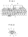
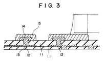
- the W-Ir combination the functions thereof will be described with reference to Figs. 1 and 2 in conjunction with an exemplified case where this W-Ir combination is used in an alumina substrate.
- Laminated alumina green sheets constituting electrically insulating ceramic layers 1 and having through holes 3 including internal conductors 2 over which a material of a W-Ir intermediate metal layer 4 is filled, as shown in Fig. 2.
- the laminated alumina green sheets are subjected to cofiring to effect solid solution of Ir into W to thereby form an alloy, while effecting solid solution of part of Ir with W in the internal conductor 2 in the interface 6 thereof to secure a firm bond.
- a paste comprising Cu as a main component for forming a thick film conductor layer 5 is applied around the W-Ir intermediate metal layer 4 in and over the through hole 3 of the alumina insulating layer 1, and then fired to effect solid solution of part of Ir with Cu in the interface 7 of the intermediate metal layer 4 with the Cu thick film to thereby form a firm bonding layer, whereby the bonding strength of the Cu thick film can be improved. Further, the amount of the component of elemental W having a strong reducing power against Cu is decreased by Ir as described hereinbefore to stabilize the sintering reaction of the Cu thick film to thereby form a thick dense surface conductor film having a high strength.
- Fig. 1 shows an example of a product according to the present invention, which comprises internal conductors 2 disposed inside a multilayer alumina substrate composed of insulating ceramic layers 1, intermediate metal layers 4 comprising W and/or Mo and at least one element selected from the group consisting of Ir, Pt, Ti, and Cr and filled in the through holes 3 of the surface layers of the multilayer substrate, and Cu thick film layers 5 formed around the through holes.
- a chip part M is finally mounted on the Cu thick film layers thorough a bonding material 8 such as solder.
- a tungsten (W) powder of 3 to 4 ⁇ m ⁇ in average particle size was admixed with an Ir powder having substantially the same particle size distribution as the W powder, and then mixed with an organic binder comprising as a main component an ethyl cellulose resin dissolved in a solvent to prepare a paste.
- the paste was filled into the through-hole portions of a surface alumina green sheet, which becomes the surface layer of a multilayered ceramic substrate after firing, by filling printing.
- a W conductive paste was filled into through holes of other alumina green sheets and then printed in internal conductor patterns onto the green sheets. The thus treated green sheets were stacked together into a laminated structure and then cofired.
- a commercially available Cu paste (#9922 manufactured by Du Pont Company) was applied on the surface layer with the through holes as centers by printing to form printed layers of 2 mm x 2 mm square in size, followed by firing to produce a product.
- the bonding strength of the product was evaluated in terms of initial strength and strength after keeping thereof at a high temperature of 150°C.
- the measurement method was as follows. The product was immersed in a molten solder bath having a temperature of 235 ⁇ 5°C. Lead wires (wire diameter: 0.6 mm ⁇ ) for a tensile test were soldered onto the lands of 2 mm x 2 mm square in size on the product. The initial bonding strength and the bonding strength after keeping at 150°C for 1,000 hours were measured by a peeling tensile test method.
- Example 1 In both of Example 1 and Comparative Example 1, the area rate of solder wetting through immersion in the molten solder bath was so good as to be problem-free in a practical aspect.
- the intermediate metal layers of the multilayer ceramic circuit substrate of the present invention even if small in area, firmly bond the surface conductors thereof to the internal conductors thereof without direct contact between the two kinds of conductors, the pitches between the through holes can be minimized to minimize the pitches between the surface conductors as well. Accordingly, chips to be mounted between the surface conductors on the substrate can be miniaturized to increase the packaging density thereof while enabling miniaturization of circuit components.
Landscapes
- Engineering & Computer Science (AREA)
- Chemical & Material Sciences (AREA)
- Inorganic Chemistry (AREA)
- Manufacturing & Machinery (AREA)
- Microelectronics & Electronic Packaging (AREA)
- Parts Printed On Printed Circuit Boards (AREA)
- Production Of Multi-Layered Print Wiring Board (AREA)
Applications Claiming Priority (2)
| Application Number | Priority Date | Filing Date | Title |
|---|---|---|---|
| JP330831/93 | 1993-12-27 | ||
| JP33083193A JP3286651B2 (ja) | 1993-12-27 | 1993-12-27 | セラミック多層配線基板およびその製造法並びにセラミック多層配線基板用導電材料 |
Publications (2)
| Publication Number | Publication Date |
|---|---|
| EP0660651A1 true EP0660651A1 (fr) | 1995-06-28 |
| EP0660651B1 EP0660651B1 (fr) | 1998-02-04 |
Family
ID=18237031
Family Applications (1)
| Application Number | Title | Priority Date | Filing Date |
|---|---|---|---|
| EP94120404A Expired - Lifetime EP0660651B1 (fr) | 1993-12-27 | 1994-12-22 | Substrat céramique à circuit multicouche, procédé de production, et matériau électriquement conducteur pour utilisation dans un substrat céramique à circuit multicouche |
Country Status (4)
| Country | Link |
|---|---|
| US (2) | US5627344A (fr) |
| EP (1) | EP0660651B1 (fr) |
| JP (1) | JP3286651B2 (fr) |
| DE (1) | DE69408432T2 (fr) |
Cited By (1)
| Publication number | Priority date | Publication date | Assignee | Title |
|---|---|---|---|---|
| EP3030061A4 (fr) * | 2013-07-29 | 2017-03-29 | Kyocera Corporation | Substrat de circuit, substrat de circuit avec conducteur, et dispositif électronique |
Families Citing this family (27)
| Publication number | Priority date | Publication date | Assignee | Title |
|---|---|---|---|---|
| JP3286651B2 (ja) * | 1993-12-27 | 2002-05-27 | 株式会社住友金属エレクトロデバイス | セラミック多層配線基板およびその製造法並びにセラミック多層配線基板用導電材料 |
| US5670750A (en) * | 1995-04-27 | 1997-09-23 | International Business Machines Corporation | Electric circuit card having a donut shaped land |
| US6195883B1 (en) * | 1998-03-25 | 2001-03-06 | International Business Machines Corporation | Full additive process with filled plated through holes |
| JP3234757B2 (ja) * | 1995-12-05 | 2001-12-04 | インターナショナル・ビジネス・マシーンズ・コーポレーション | 多層配線基板及びその製造方法 |
| JP2736042B2 (ja) * | 1995-12-12 | 1998-04-02 | 山一電機株式会社 | 回路基板 |
| JP3704864B2 (ja) | 1997-02-12 | 2005-10-12 | 株式会社デンソー | 半導体素子の実装構造 |
| JPH10308582A (ja) * | 1997-05-07 | 1998-11-17 | Denso Corp | 多層配線基板 |
| JP3709752B2 (ja) * | 1999-01-26 | 2005-10-26 | 株式会社村田製作所 | 誘電体セラミック組成物及びセラミック多層基板 |
| US6930395B2 (en) * | 2000-12-05 | 2005-08-16 | Matsushita Electric Industrial Co., Ltd. | Circuit substrate having improved connection reliability and a method for manufacturing the same |
| US6800815B1 (en) | 2001-01-16 | 2004-10-05 | National Semiconductor Corporation | Materials and structure for a high reliability bga connection between LTCC and PB boards |
| US6762369B2 (en) * | 2001-10-29 | 2004-07-13 | Matsushita Electric Industrial Co., Ltd. | Multilayer ceramic substrate and method for manufacturing the same |
| US7222419B2 (en) * | 2001-12-19 | 2007-05-29 | Chung-Shan Institute Of Science And Technology | Method of fabricating a ceramic substrate with a thermal conductive plug of a multi-chip package |
| WO2003101166A1 (fr) * | 2002-05-28 | 2003-12-04 | Sumitomo Electric Industries, Ltd. | Pastille frittee a base de nitrure d'aluminium comportant une couche metallisee et procede de preparation associe |
| US6900395B2 (en) * | 2002-11-26 | 2005-05-31 | International Business Machines Corporation | Enhanced high-frequency via interconnection for improved reliability |
| DE102004032706A1 (de) * | 2004-07-06 | 2006-02-02 | Epcos Ag | Verfahren zur Herstellung eines elektrischen Bauelements und das Bauelement |
| US20060021792A1 (en) * | 2004-07-28 | 2006-02-02 | Myers Bruce A | Surface mount axial leaded component for an electronic module |
| EP1666161A1 (fr) * | 2004-11-25 | 2006-06-07 | Nederlandse Organisatie voor toegepast-natuurwetenschappelijk Onderzoek TNO | Système d'absorption d'overspray |
| US7650694B2 (en) * | 2005-06-30 | 2010-01-26 | Intel Corporation | Method for forming multilayer substrate |
| TW200920215A (en) * | 2007-10-17 | 2009-05-01 | Murata Manufacturing Co | Multilayer ceramic substrate and process for producing the multilayer ceramic |
| KR100896610B1 (ko) * | 2007-11-05 | 2009-05-08 | 삼성전기주식회사 | 다층 세라믹 기판 및 그 제조방법 |
| KR20110019536A (ko) * | 2009-08-20 | 2011-02-28 | 삼성전기주식회사 | 세라믹 기판 및 그 제조방법 |
| KR101101574B1 (ko) * | 2009-09-18 | 2012-01-02 | 삼성전기주식회사 | 세라믹 기판 및 그의 제조 방법 |
| CN103477727B (zh) * | 2011-03-28 | 2016-08-31 | 株式会社村田制作所 | 玻璃陶瓷基板及其制造方法 |
| KR20140024584A (ko) * | 2012-08-20 | 2014-03-03 | 삼성전기주식회사 | 내부전극용 도전성 페이스트 조성물 및 이를 포함하는 적층 세라믹 전자부품 |
| KR102093157B1 (ko) * | 2014-12-01 | 2020-03-25 | 삼성전기주식회사 | 다층 세라믹 기판 |
| SG11201703892PA (en) * | 2014-12-09 | 2017-06-29 | Intel Corp | Microelectronic substrates having copper alloy conductive route structures |
| CN105934085A (zh) * | 2016-06-28 | 2016-09-07 | 广东欧珀移动通信有限公司 | Pcb板及具有其的移动终端 |
Citations (7)
| Publication number | Priority date | Publication date | Assignee | Title |
|---|---|---|---|---|
| GB2149222A (en) * | 1983-09-16 | 1985-06-05 | Matsushita Electric Industrial Co Ltd | Multilatered ceramic substrate and method of making the same |
| US4529835A (en) * | 1982-10-23 | 1985-07-16 | Ngk Insulators, Ltd. | Ceramic thick film circuit substrate |
| JPS62123795A (ja) * | 1985-11-25 | 1987-06-05 | 株式会社東芝 | 配線基板 |
| US4861641A (en) * | 1987-05-22 | 1989-08-29 | Ceramics Process Systems Corporation | Substrates with dense metal vias |
| JPH03196696A (ja) * | 1989-12-26 | 1991-08-28 | Kyocera Corp | 回路基板 |
| JPH03218693A (ja) * | 1988-12-23 | 1991-09-26 | Narumi China Corp | セラミック多層配線基板およびその製造方法 |
| US5156903A (en) * | 1989-12-21 | 1992-10-20 | Sumitomo Metal Ceramics Inc. | Multilayer ceramic substrate and manufacture thereof |
Family Cites Families (12)
| Publication number | Priority date | Publication date | Assignee | Title |
|---|---|---|---|---|
| DE2742534C2 (de) * | 1977-09-21 | 1985-01-24 | Siemens AG, 1000 Berlin und 8000 München | Verbindungselement für elektronische Schaltungen |
| US4685030A (en) * | 1985-04-29 | 1987-08-04 | Energy Conversion Devices, Inc. | Surface mounted circuits including hybrid circuits, having CVD interconnects, and method of preparing the circuits |
| EP0235682B2 (fr) * | 1986-02-20 | 1997-11-12 | Kabushiki Kaisha Toshiba | Corps frité à base de nitrure d'aluminium, muni d'une couche métallisée conductrice |
| JPH0714105B2 (ja) * | 1986-05-19 | 1995-02-15 | 日本電装株式会社 | 混成集積回路基板及びその製造方法 |
| DE3924225C2 (de) * | 1988-07-22 | 1994-01-27 | Mitsubishi Electric Corp | Verfahren zur Herstellung eines Keramik-Metall-Verbundsubstrats sowie Keramik-Metall-Verbundsubstrat |
| US5031308A (en) * | 1988-12-29 | 1991-07-16 | Japan Radio Co., Ltd. | Method of manufacturing multilayered printed-wiring-board |
| JPH05183273A (ja) * | 1990-09-07 | 1993-07-23 | Hitachi Ltd | 多層配線基板装置とその製造方法ならびにそれを用いた電子装置 |
| JPH05218646A (ja) * | 1992-02-05 | 1993-08-27 | Ngk Insulators Ltd | 薄膜多層配線基板の製造方法 |
| US5259110A (en) * | 1992-04-03 | 1993-11-09 | International Business Machines Corporation | Method for forming a multilayer microelectronic wiring module |
| US5329695A (en) * | 1992-09-01 | 1994-07-19 | Rogers Corporation | Method of manufacturing a multilayer circuit board |
| JP3237258B2 (ja) * | 1993-01-22 | 2001-12-10 | 株式会社デンソー | セラミック多層配線基板 |
| JP3286651B2 (ja) * | 1993-12-27 | 2002-05-27 | 株式会社住友金属エレクトロデバイス | セラミック多層配線基板およびその製造法並びにセラミック多層配線基板用導電材料 |
-
1993
- 1993-12-27 JP JP33083193A patent/JP3286651B2/ja not_active Expired - Lifetime
-
1994
- 1994-12-22 EP EP94120404A patent/EP0660651B1/fr not_active Expired - Lifetime
- 1994-12-22 US US08/362,129 patent/US5627344A/en not_active Expired - Lifetime
- 1994-12-22 DE DE69408432T patent/DE69408432T2/de not_active Expired - Fee Related
-
1995
- 1995-11-22 US US08/561,539 patent/US5729893A/en not_active Expired - Lifetime
Patent Citations (7)
| Publication number | Priority date | Publication date | Assignee | Title |
|---|---|---|---|---|
| US4529835A (en) * | 1982-10-23 | 1985-07-16 | Ngk Insulators, Ltd. | Ceramic thick film circuit substrate |
| GB2149222A (en) * | 1983-09-16 | 1985-06-05 | Matsushita Electric Industrial Co Ltd | Multilatered ceramic substrate and method of making the same |
| JPS62123795A (ja) * | 1985-11-25 | 1987-06-05 | 株式会社東芝 | 配線基板 |
| US4861641A (en) * | 1987-05-22 | 1989-08-29 | Ceramics Process Systems Corporation | Substrates with dense metal vias |
| JPH03218693A (ja) * | 1988-12-23 | 1991-09-26 | Narumi China Corp | セラミック多層配線基板およびその製造方法 |
| US5156903A (en) * | 1989-12-21 | 1992-10-20 | Sumitomo Metal Ceramics Inc. | Multilayer ceramic substrate and manufacture thereof |
| JPH03196696A (ja) * | 1989-12-26 | 1991-08-28 | Kyocera Corp | 回路基板 |
Non-Patent Citations (3)
| Title |
|---|
| DATABASE WPI Week 8728, Derwent World Patents Index; AN 87-194926 * |
| J.J. GNIEWEK ET AL.: "Metallurgy for multilayer ceramic modules", IBM TECHNICAL DISCLOSURE BULLETIN., vol. 18, no. 9, February 1976 (1976-02-01), NEW YORK US, pages 2856 - 2857 * |
| PATENT ABSTRACTS OF JAPAN vol. 15, no. 459 (E - 1136) 21 November 1991 (1991-11-21) * |
Cited By (1)
| Publication number | Priority date | Publication date | Assignee | Title |
|---|---|---|---|---|
| EP3030061A4 (fr) * | 2013-07-29 | 2017-03-29 | Kyocera Corporation | Substrat de circuit, substrat de circuit avec conducteur, et dispositif électronique |
Also Published As
| Publication number | Publication date |
|---|---|
| DE69408432D1 (de) | 1998-03-12 |
| US5627344A (en) | 1997-05-06 |
| JPH07193372A (ja) | 1995-07-28 |
| JP3286651B2 (ja) | 2002-05-27 |
| DE69408432T2 (de) | 1998-05-20 |
| US5729893A (en) | 1998-03-24 |
| EP0660651B1 (fr) | 1998-02-04 |
Similar Documents
| Publication | Publication Date | Title |
|---|---|---|
| EP0660651B1 (fr) | Substrat céramique à circuit multicouche, procédé de production, et matériau électriquement conducteur pour utilisation dans un substrat céramique à circuit multicouche | |
| US5439732A (en) | Ceramic multi-layer wiring board | |
| US6261703B1 (en) | Copper circuit junction substrate and method of producing the same | |
| US7804677B2 (en) | Electronic component and method for producing the same | |
| EP0278741B1 (fr) | Parties de composants électroniques et procédé pour leur fabrication | |
| US7362560B2 (en) | Multilayer electronic component and method for producing the same | |
| DE69736144T2 (de) | Teil für Halbleiter aus Aluminiumnitrid-Substratmaterial und seine Herstellungsmethode | |
| JPS5852900A (ja) | セラミツク多層配線板の製造方法 | |
| US6338893B1 (en) | Conductive paste and ceramic printed circuit substrate using the same | |
| JPH04169002A (ja) | 導電性ペーストとそれを用いた多層セラミック配線基板の製造方法 | |
| US6335077B1 (en) | Electrically conductive paste for via-hole and method of producing monolithic ceramic substrate using the same | |
| JP2002290052A (ja) | 多層配線基板 | |
| JP4038602B2 (ja) | 導電性ペースト及びセラミック多層基板 | |
| JP3167796B2 (ja) | セラミックス回路基板 | |
| JP2001155955A (ja) | 外部端子電極具備電子部品及びその搭載電子用品 | |
| KR100744855B1 (ko) | 높은 열적 사이클 전도체 시스템 | |
| JPH06334351A (ja) | 導体ペーストおよびそれを用いたセラミック多層配線基板 | |
| JP2738600B2 (ja) | 回路基板 | |
| JPH01201090A (ja) | セラミック用メタライズ組成物 | |
| JP2703426B2 (ja) | 回路基板 | |
| JP2000022294A (ja) | 電子部品回路基板 | |
| JPH08274422A (ja) | 回路基板 | |
| JPH03116608A (ja) | 導体ペーストおよび導体 | |
| JP2842707B2 (ja) | 回路基板 | |
| JP3145614B2 (ja) | セラミック配線基板 |
Legal Events
| Date | Code | Title | Description |
|---|---|---|---|
| PUAI | Public reference made under article 153(3) epc to a published international application that has entered the european phase |
Free format text: ORIGINAL CODE: 0009012 |
|
| AK | Designated contracting states |
Kind code of ref document: A1 Designated state(s): DE FR GB |
|
| 17P | Request for examination filed |
Effective date: 19950704 |
|
| RAP1 | Party data changed (applicant data changed or rights of an application transferred) |
Owner name: NIPPONDENSO CO., LTD. Owner name: SUMITOMO METAL CERAMICS INC. |
|
| 17Q | First examination report despatched |
Effective date: 19951211 |
|
| GRAG | Despatch of communication of intention to grant |
Free format text: ORIGINAL CODE: EPIDOS AGRA |
|
| RAP1 | Party data changed (applicant data changed or rights of an application transferred) |
Owner name: NIPPONDENSO CO., LTD. Owner name: SUMITOMO METAL (SMI) ELECTRONICS DEVICES INC. |
|
| GRAG | Despatch of communication of intention to grant |
Free format text: ORIGINAL CODE: EPIDOS AGRA |
|
| GRAH | Despatch of communication of intention to grant a patent |
Free format text: ORIGINAL CODE: EPIDOS IGRA |
|
| GRAH | Despatch of communication of intention to grant a patent |
Free format text: ORIGINAL CODE: EPIDOS IGRA |
|
| RAP1 | Party data changed (applicant data changed or rights of an application transferred) |
Owner name: DENSO CORPORATION Owner name: SUMITOMO METAL (SMI) ELECTRONICS DEVICES INC. |
|
| GRAA | (expected) grant |
Free format text: ORIGINAL CODE: 0009210 |
|
| AK | Designated contracting states |
Kind code of ref document: B1 Designated state(s): DE FR GB |
|
| REF | Corresponds to: |
Ref document number: 69408432 Country of ref document: DE Date of ref document: 19980312 |
|
| ET | Fr: translation filed | ||
| PLBE | No opposition filed within time limit |
Free format text: ORIGINAL CODE: 0009261 |
|
| STAA | Information on the status of an ep patent application or granted ep patent |
Free format text: STATUS: NO OPPOSITION FILED WITHIN TIME LIMIT |
|
| 26N | No opposition filed | ||
| PGFP | Annual fee paid to national office [announced via postgrant information from national office to epo] |
Ref country code: GB Payment date: 20001115 Year of fee payment: 7 |
|
| PGFP | Annual fee paid to national office [announced via postgrant information from national office to epo] |
Ref country code: FR Payment date: 20001204 Year of fee payment: 7 |
|
| PGFP | Annual fee paid to national office [announced via postgrant information from national office to epo] |
Ref country code: DE Payment date: 20001213 Year of fee payment: 7 |
|
| PG25 | Lapsed in a contracting state [announced via postgrant information from national office to epo] |
Ref country code: GB Free format text: LAPSE BECAUSE OF NON-PAYMENT OF DUE FEES Effective date: 20011222 |
|
| REG | Reference to a national code |
Ref country code: GB Ref legal event code: IF02 |
|
| PG25 | Lapsed in a contracting state [announced via postgrant information from national office to epo] |
Ref country code: DE Free format text: LAPSE BECAUSE OF NON-PAYMENT OF DUE FEES Effective date: 20020702 |
|
| GBPC | Gb: european patent ceased through non-payment of renewal fee |
Effective date: 20011222 |
|
| PG25 | Lapsed in a contracting state [announced via postgrant information from national office to epo] |
Ref country code: FR Free format text: LAPSE BECAUSE OF NON-PAYMENT OF DUE FEES Effective date: 20020830 |
|
| REG | Reference to a national code |
Ref country code: FR Ref legal event code: ST |