EP0661761A2 - Herstellungsverfahren für einen photoelektrischen Umwandler - Google Patents
Herstellungsverfahren für einen photoelektrischen Umwandler Download PDFInfo
- Publication number
- EP0661761A2 EP0661761A2 EP94309905A EP94309905A EP0661761A2 EP 0661761 A2 EP0661761 A2 EP 0661761A2 EP 94309905 A EP94309905 A EP 94309905A EP 94309905 A EP94309905 A EP 94309905A EP 0661761 A2 EP0661761 A2 EP 0661761A2
- Authority
- EP
- European Patent Office
- Prior art keywords
- substrate
- layer
- type layer
- manufacturing
- photoelectric transducer
- Prior art date
- Legal status (The legal status is an assumption and is not a legal conclusion. Google has not performed a legal analysis and makes no representation as to the accuracy of the status listed.)
- Withdrawn
Links
Images


Classifications
-
- H—ELECTRICITY
- H10—SEMICONDUCTOR DEVICES; ELECTRIC SOLID-STATE DEVICES NOT OTHERWISE PROVIDED FOR
- H10F—INORGANIC SEMICONDUCTOR DEVICES SENSITIVE TO INFRARED RADIATION, LIGHT, ELECTROMAGNETIC RADIATION OF SHORTER WAVELENGTH OR CORPUSCULAR RADIATION
- H10F71/00—Manufacture or treatment of devices covered by this subclass
- H10F71/10—Manufacture or treatment of devices covered by this subclass the devices comprising amorphous semiconductor material
- H10F71/107—Continuous treatment of the devices, e.g. roll-to roll processes or multi-chamber deposition
-
- H—ELECTRICITY
- H10—SEMICONDUCTOR DEVICES; ELECTRIC SOLID-STATE DEVICES NOT OTHERWISE PROVIDED FOR
- H10F—INORGANIC SEMICONDUCTOR DEVICES SENSITIVE TO INFRARED RADIATION, LIGHT, ELECTROMAGNETIC RADIATION OF SHORTER WAVELENGTH OR CORPUSCULAR RADIATION
- H10F10/00—Individual photovoltaic cells, e.g. solar cells
- H10F10/10—Individual photovoltaic cells, e.g. solar cells having potential barriers
- H10F10/17—Photovoltaic cells having only PIN junction potential barriers
- H10F10/172—Photovoltaic cells having only PIN junction potential barriers comprising multiple PIN junctions, e.g. tandem cells
-
- H—ELECTRICITY
- H10—SEMICONDUCTOR DEVICES; ELECTRIC SOLID-STATE DEVICES NOT OTHERWISE PROVIDED FOR
- H10F—INORGANIC SEMICONDUCTOR DEVICES SENSITIVE TO INFRARED RADIATION, LIGHT, ELECTROMAGNETIC RADIATION OF SHORTER WAVELENGTH OR CORPUSCULAR RADIATION
- H10F71/00—Manufacture or treatment of devices covered by this subclass
- H10F71/10—Manufacture or treatment of devices covered by this subclass the devices comprising amorphous semiconductor material
- H10F71/103—Manufacture or treatment of devices covered by this subclass the devices comprising amorphous semiconductor material including only Group IV materials
-
- H—ELECTRICITY
- H10—SEMICONDUCTOR DEVICES; ELECTRIC SOLID-STATE DEVICES NOT OTHERWISE PROVIDED FOR
- H10F—INORGANIC SEMICONDUCTOR DEVICES SENSITIVE TO INFRARED RADIATION, LIGHT, ELECTROMAGNETIC RADIATION OF SHORTER WAVELENGTH OR CORPUSCULAR RADIATION
- H10F71/00—Manufacture or treatment of devices covered by this subclass
- H10F71/10—Manufacture or treatment of devices covered by this subclass the devices comprising amorphous semiconductor material
- H10F71/103—Manufacture or treatment of devices covered by this subclass the devices comprising amorphous semiconductor material including only Group IV materials
- H10F71/1035—Manufacture or treatment of devices covered by this subclass the devices comprising amorphous semiconductor material including only Group IV materials having multiple Group IV elements, e.g. SiGe or SiC
-
- H—ELECTRICITY
- H10—SEMICONDUCTOR DEVICES; ELECTRIC SOLID-STATE DEVICES NOT OTHERWISE PROVIDED FOR
- H10F—INORGANIC SEMICONDUCTOR DEVICES SENSITIVE TO INFRARED RADIATION, LIGHT, ELECTROMAGNETIC RADIATION OF SHORTER WAVELENGTH OR CORPUSCULAR RADIATION
- H10F77/00—Constructional details of devices covered by this subclass
- H10F77/10—Semiconductor bodies
- H10F77/16—Material structures, e.g. crystalline structures, film structures or crystal plane orientations
- H10F77/169—Thin semiconductor films on metallic or insulating substrates
- H10F77/1692—Thin semiconductor films on metallic or insulating substrates the films including only Group IV materials
-
- H—ELECTRICITY
- H10—SEMICONDUCTOR DEVICES; ELECTRIC SOLID-STATE DEVICES NOT OTHERWISE PROVIDED FOR
- H10F—INORGANIC SEMICONDUCTOR DEVICES SENSITIVE TO INFRARED RADIATION, LIGHT, ELECTROMAGNETIC RADIATION OF SHORTER WAVELENGTH OR CORPUSCULAR RADIATION
- H10F77/00—Constructional details of devices covered by this subclass
- H10F77/40—Optical elements or arrangements
- H10F77/42—Optical elements or arrangements directly associated or integrated with photovoltaic cells, e.g. light-reflecting means or light-concentrating means
- H10F77/48—Back surface reflectors [BSR]
-
- Y—GENERAL TAGGING OF NEW TECHNOLOGICAL DEVELOPMENTS; GENERAL TAGGING OF CROSS-SECTIONAL TECHNOLOGIES SPANNING OVER SEVERAL SECTIONS OF THE IPC; TECHNICAL SUBJECTS COVERED BY FORMER USPC CROSS-REFERENCE ART COLLECTIONS [XRACs] AND DIGESTS
- Y02—TECHNOLOGIES OR APPLICATIONS FOR MITIGATION OR ADAPTATION AGAINST CLIMATE CHANGE
- Y02E—REDUCTION OF GREENHOUSE GAS [GHG] EMISSIONS, RELATED TO ENERGY GENERATION, TRANSMISSION OR DISTRIBUTION
- Y02E10/00—Energy generation through renewable energy sources
- Y02E10/50—Photovoltaic [PV] energy
- Y02E10/52—PV systems with concentrators
-
- Y—GENERAL TAGGING OF NEW TECHNOLOGICAL DEVELOPMENTS; GENERAL TAGGING OF CROSS-SECTIONAL TECHNOLOGIES SPANNING OVER SEVERAL SECTIONS OF THE IPC; TECHNICAL SUBJECTS COVERED BY FORMER USPC CROSS-REFERENCE ART COLLECTIONS [XRACs] AND DIGESTS
- Y02—TECHNOLOGIES OR APPLICATIONS FOR MITIGATION OR ADAPTATION AGAINST CLIMATE CHANGE
- Y02E—REDUCTION OF GREENHOUSE GAS [GHG] EMISSIONS, RELATED TO ENERGY GENERATION, TRANSMISSION OR DISTRIBUTION
- Y02E10/00—Energy generation through renewable energy sources
- Y02E10/50—Photovoltaic [PV] energy
- Y02E10/548—Amorphous silicon PV cells
-
- Y—GENERAL TAGGING OF NEW TECHNOLOGICAL DEVELOPMENTS; GENERAL TAGGING OF CROSS-SECTIONAL TECHNOLOGIES SPANNING OVER SEVERAL SECTIONS OF THE IPC; TECHNICAL SUBJECTS COVERED BY FORMER USPC CROSS-REFERENCE ART COLLECTIONS [XRACs] AND DIGESTS
- Y02—TECHNOLOGIES OR APPLICATIONS FOR MITIGATION OR ADAPTATION AGAINST CLIMATE CHANGE
- Y02P—CLIMATE CHANGE MITIGATION TECHNOLOGIES IN THE PRODUCTION OR PROCESSING OF GOODS
- Y02P70/00—Climate change mitigation technologies in the production process for final industrial or consumer products
- Y02P70/50—Manufacturing or production processes characterised by the final manufactured product
Definitions
- the present invention relates to a method of manufacturing a photoelectric transducer, more specifically relates to a method of manufacturing a photoelectric transducer which comprises a metal film as light-reflecting layer on a conductive substrate and semiconductor thereon comprising non-monocrystalline material containing silicon atom as the matrix.
- a method of manufacturing a photoelectric transducer that forms a photovoltaic device in a high yield, uniform and durable for a long period use.
- Such solar cells are based on a technology using photovoltaic effect of pn junction and others in the functional part.
- Semiconductor materials which constitutes the pn junction generally are silicon and germanium. Such semiconductors like silicon absorb sunlight and generate electron and hole photo-carriers, which are drifted by the internal electric field of the pn junction to outside.
- a crystalline silicon like monocrystal has indirect optical ends and its absorption of light is small; thus, it has disadvantages in that a solar cell of monocrystalline silicon has to be of at least 50 microns thickness for absorbing incident sunlight and that short wave components are not effectively used because the band gap is about 1.1 eV which is narrower than 1.5 eV suitable as a solar cell.
- a polycrystalline silicon Even if a polycrystalline silicon is used for lowering the production cost, thickness of the solar cell cannot be decreased because the problem of indirect optical ends remains unsolved. Furthermore, a polycrystalline silicon also has other problems like grain boundary. It is generally recognized that a fine crystalline silicon and an amorphous silicon derived material is advantageous which is non-monocrystalline and formed by a chemical vapor deposition (CVD) method for the purpose of making the area large and lowering the cost. While amorphous silicon solar cells, which are of non-monocrystalline semiconductors and able to be made into thin films, have been prevalent as small power sources for living goods, problems in efficiency and stabilization have to be overcome for the use as electric power cells.
- the inventors have studied on non-monocrystalline silicon solar cell formed on a conductive substrate and recognized the importance of the conductive substrate and the interface conditions of the metal layer and others formed thereon. Thereby, the inventors have found that poor adherence, existence of impurity, and poor junction make the conversion efficiency of the solar cell lowered and bring deterioration of the reliability, durability and production yield. It means the cleaning method of the conductive substrate is very important, however, conventional cleaning method of the substrate has been merely tried to be improved by the use of a solvent or washing with water.
- the photoelectric transducer manufactured by a method that comprises forming, on a conductive substrate, a metal layer as light-reflecting layer, a reflection enhancing layer thereon, and semiconductor photovolatic layer comprising of a non-monocrystalline material containing silicon atom as the matrix by a plasma CVD method, has layers of relatively thin films; its manufacturing method comprises many steps where the temperature is relatively high. Therefore, the adhesion between the conductive substrate and the metal layer formed thereon, the presence of impurities, the conditions of junction are very important for improving the conversion efficiency of photoelectric transducer, the reliability, and the manufacturing yield.
- An object of the present invention is to provide a manufacturing method whereby photoelectric transducers having a high conversion efficiency and long life durable for use for a long period are manufactured constantly, stably, and in a high yield by overcoming problems as mentioned above associated with conventional manufacturing methods of photoelectric transducers.
- Another object of the present invention is to provide a manufacturing method whereby photoelectric transducers of high durability including moisture resistance are manufactured constantly, stably, and in a high yield.
- Another object of the present invention is to provide a manufacturing method whereby photoelectric transducers of high reliability resisting deformation such as deformation of the substrate are manufactured constantly, stably, and in a high yield.
- Another object of the present invention is to provide a manufacturing method of photoelectric transducers, of excellent uniformity, being able to be incorporated into a large area are manufactured.
- Another object of the present invention is to provide an environment-friendly manufacturing method of photoelectric transducers wherein organic solvents are not used.
- Another object of the present invention is to provide a manufacturing method of photoelectric transducers excellent in mass continuous production at low cost.
- the method of manufacturing a photoelectric transducer according to the present invention is to manufacture a photoelectric transducer in which a functional film is formed on a conductive substrate which comprises applying ultrasonic cleaning with a cleaning liquid containing water to the conductive substrate surface, thereafter allowing the surface of the conductive substrate to contact with purified water, and followed by forming the functional film.
- the functional film is characterized in being formed by a metal layer as light-reflecting layer, a reflection enhancing layer, and a semiconductor photovolatic layer, formed by a plasma CVD method, comprising a non-monocrystalline material containing silicon atom as the matrix.
- Fig. 1 is a schematic cross sectional view illustrating a cleaning step of a conductive substrate in the method of manufacturing a photoelectric transducer according to the present invention.
- Fig. 2 is a schematic cross sectional view illustrating a device forming a light-reflecting layer and reflection enhancing layer according to the present invention.
- Fig. 3 is a schematic cross sectional view illustrating constitution of a photoelectric transducer.
- Fig. 4 is a schematic cross sectional view illustrating an example of plasma CVD apparatus.
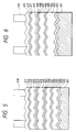
- Fig. 5 is a schematic cross sectional view illustrating constitution of a triple type solar cell.
- Fig. 6 is a schematic cross sectional view illustrating constitution of a tandem type solar cell.
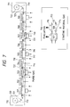
- Fig. 7 is a schematic drawing illustrating an example of deposition apparatus of roll-to-roll type.
- the inventors have noted on the possibility of improving the conversion efficiency, reliability, and yield by means of some treatment to the substrate surface prior to the formation of a metal layer as a light-reflecting layer on a conductive substrate; a concentrated study in this regard has led completion of the present invention. While mechanism of the present invention is not clear, the inventors understand at present as follows. First, impurities and fine particles remaining on a conductive substrate cause poor adhesion, defects due to insufficient coverage, increase of resistance in series, poor yield, and peeling off of the films in a continuous use. Too much existence of such impurities and fine particles cause significant lowering of conversion efficiency, reliability and yield, which existence is a conspicuous and important problem in the photoelectric transducer in the constituents of the present invention.
- a combination of solvents having high cleaning capability is required above all when a cleaning method, conventionally frequently used, using solvents is applied to a conductive substrate.
- This method is not practical, however, in consideration of the purity and amount of the solvents employed and economy since there are many problems such as adhesion of fine particles of micron and submicron order size, repeated adhesion of impurities, and local adhesion of fine particles and impurities due to short drying period of the solvents in general.
- the cleaning liquid containing water which has a high dispersion ability, is used in the ultrasonic cleaning removing impurities adhered to the conductive substrate effectively.
- the adhered impurities are metallic powder or the like, water is enough for the cleaning liquid.
- the adhered impurities include oil and fat, preferable cleaning liquid contains a surfactant added to water.
- the conductive substrate applied the ultrasonic cleaning is sent without being dried to a contact step with purified water, wherein the impurities hardly adhere repeatedly; the contact is effectively made to the purified of high resistivity water almost free of fine particles wherein the impurities including the surfactant are removed. In this way, the surface of conductive substrate becomes in good conditions for the photoelectric transducer composed in the constituents according to the present invention.
- the combination of the step of applying ultrasonic cleaning with a cleaning liquid containing water to the conductive substrate surface and the step of allowing the cleaned surface of the conductive substrate to contact with purified water makes the grain boundary condition in the surface of conductive substrate in good conditions for the photoelectric transducer composed in the constituents according to the present invention.
- thinly etching has been applied to a conductive substrate surface by use of an acid, however, this etching is not suitable for the photoelectric transducer in the constituents according to the present invention since the grain boundary condition becomes excessively coarse.
- the effect of the ultrasonic wave in the cleaning step and the effect of the water pressure in the purified water contact step mainly make the substrate surface in good conditions; thereby adhesion between the conductive substrate and the metal layer is improved and the resistance in series becomes lowered.
- the combination of the step of applying ultrasonic cleaning with a cleaning liquid containing water to the conductive substrate surface and the step of allowing the cleaned surface of the conductive substrate to contact with purified water brings an effect to make the oxidation condition of the conductive substrate surface uniform.
- the adhesion becomes uniform and resistant to some deformation of the substrate and the junction conditions hardly change with elapse of time, giving excellent durability and reliance.
- Existence of oxide film may theoretically increase the resistance in series, however, it does not cause practical problems according to the present invention since the formed oxide film is extremely thin.
- junction between the conductive substrate and the metal layer is realized according to the present invention having excellent and uniform adhesion and junction condition free of change with elapse of time even when integrated in a large area.
- This makes it possible to make respective layers thinner and to form layers at elevated temperatures.
- a photoelectric transducer stably, constantly and in a high yield that has a high conversion efficiency, long service life, high humidity resistance, reliable resistance to the substrate deformation, and other excellent quality characteristics.
- An organic solvent is not used in the manufacturing method; therefore environment-friendly and low cost manufacture is possible. Furthermore, the excellent effects are easily kept for a large volume and continuous treatment by the cleaning function which contains water and has high dispersion capability.
- the cleaning liquid used in the cleaning step of the present invention is preferably water or water containing a surfactant as the cleaning liquid containing water.
- water quality is acceptable as the cleaning water to which a surfactant is added
- most preferable water is purified water of semiconductor grade. More specifically, water having resistivity at 25°C of at least 1 M ⁇ cm, preferably 5 M ⁇ cm or higher, and most preferably 10 M ⁇ cm or higher is suitable for the purpose of the present invention.
- the upper limit of the resistivity may be any value up to the theoretical resistivity of 18.25 M ⁇ cm, however, 18.2 M ⁇ cm or lower, preferably 18.0 M ⁇ cm or lower, and most preferably 17.8 M ⁇ cm or lower is suitable for the purpose of the present invention in view of cost and productivity.
- Amount of the fine particles of 0.2 ⁇ m size or larger in the water pertinent to the present invention is 10000 per milliliter or less, preferably 1000 per milliliter or less, and most preferably 100 per milliliter or less.
- Microbes in the water pertinent to the present invention is 100 per milliliter or less, preferably 10 per milliliter or less, and most preferably 1 per milliliter or less.
- Activated carbon, distillation, ion-exchange, filtration with filter, reverse osmosis, and ultraviolet sterilization are applicable for getting the cleaning liquid containing water mentioned above; combination of a plurality of these methods are preferred to improve the water quality to the required level.
- the water temperature for the present invention purpose is 10°C to 90°C, preferably 20°C to 75°C, and most preferably 30°C to 55°C.
- the surfactant employed in the cleaning step of the present invention may be anyone of anionic, nonionic, amphoteric or a mixture thereof; an additive such as sodium tripolyphosphate may be added therein.
- ultrasonic wave in the cleaning step of the present invention is especially important for attaining the effect of the present invention.
- a magnetostrictive piezoelectric transducer such as of ferrite is used as the ultrasonic wave generator. Ways to introduce ultrasonic wave may be to place such into liquid in the cleaning bath, to adhere the piezoelectric transducer to the bottom or wall surface of the bath, and to transmit the ultrasonic wave to the bath by means of horn from a piezoelectric transducer installed nearby.
- Use of a plurality of piezoelectric transducers is effective for one cleaning bath is effective in adjustment of the output and uniformilization of the cleaning effect.
- Relatively low frequency ultrasonic wave of strong cavitation, has been conventionally used because of the large cleaning effect, however, such low frequency is not preferred in the present invention since the substrate is physically damaged.
- relatively high frequency is not practical in the present invention since the cleaning effect is low.
- pertinent frequency in the present invention is 10 kHz to 10 MHz, preferably 35 kHz to 5 MHz, and most preferably 50 kHz to 1 MHz.
- Pertinent output of the ultrasonic wave is preferably 0.1 W/liter to 500 W/liter, and more preferably 1 W/liter to 100 W/liter.
- Quality of the water used in the purified water contact step according to the present invention is very important and is preferably of super purified water of semiconductor grade, especially preferably of very large scale integration (LSI) grade. More specifically, water having resistivity at 25°C of at least 11 M ⁇ cm, preferably 13 M ⁇ cm or higher, and most preferably 15 M ⁇ cm or higher is suitable for the purpose of the present invention.
- the upper limit of the resistivity may be any value up to the theoretical resistivity of 18.25 M ⁇ cm, however, 18.2 M ⁇ cm or lower, preferably 18.0 M ⁇ cm or lower, and most preferably 17.8 M ⁇ cm or lower is suitable for the purpose of the present invention in view of cost and productivity.
- Amount of the fine particles of 0.2 ⁇ m size or larger in the water pertinent to the present invention is 10000 per milliliter or less, preferably 1000 per milliliter or less, and most preferably 100 per milliliter or less.
- Microbes in the water pertinent to the present invention is 100 per milliliter or less, preferably 10 per milliliter or less, and most preferably 1 per milliliter or less.
- Total organic compounds (TOC) in the water pertinent to the present invention is 10 mg per milliliter or less, preferably 1 mg per milliliter or less, and most preferably 0.2 mg per milliliter or less.
- Activated carbon, distillation, ion-exchange, filtration with filter, reverse osmosis, and ultraviolet sterilization are applicable for getting the cleaning liquid containing water mentioned above; combination of a plurality of these methods are preferred to improve the water quality to the required level.
- the contact of purified water with the substrate is preferably made with an angle in relation to the substrate surface under pressure.
- the angle is large, fouled water may adhere again; when the angle is small, the water pressure by spraying cannot be effective requiring a large amount of purified water with the poor utilization efficiency of the purified water.
- the spraying angle in relation to the substrate horizontal surface is 10 to 80 degrees, preferably 20 to 60 degrees, and most preferably 30 to 45 degrees for the purpose of the present invention.
- the spray pressure of the purified water gives small effect if too weak, and damaged the substrate physically if too strong; and should be 1 to 300 kgf/cm2, preferably 5 to 200 kgf/cm2,and most preferably 10 to 150 kgf/cm2 for the purpose of the present invention.
- the pressure unit kgf/cm2 herein means gravity kilogram per square centimeter; 1 kgf/cm2 equals 98066.5 Pa.
- Spraying method of the purified water may be nozzle spraying of high pressure purified water boosted by a pump, or nozzle spraying of mixture of high pressure air and pumped purified water under the pressure of air.
- the flow rate of purified water pertinent to the present invention in view of the effect of the invention and economy is 1 to 200 liters per minute, preferably 2 to 100 liters per minute, and most preferably 5 to 50 liters per minute.
- pertinent purified water temperature in the present invention is 5°C to 90°C, preferably 10°C to 55°C, and most preferably 15°C to 40°C.
- Fig. 1 shows a pretreatment apparatus for cleaning a substrate according to the present invention
- Fig. 2 shows a deposited film forming apparatus according to the present invention where a metal or others are deposited on the substrate
- Fig. 7 shows a deposited film forming apparatus where deposited films are formed on the substrate that has been subjected to treatments by the ways shown in Figs. 1 and 2.
- the substrate is a long stainless steel both surfaces of which are mirror polished.
- a conductive substrate 102 set in a substrate feeding mechanism 101 (wound on a roll for example) is transported continuously or intermittently to a substrate cleaning bath 111 by means of a substrate takeup mechanism 103.
- Impurities adhered on the substrate surfaces are cleaned in a cleaning liquid (aqueous surfactant solution) 112 by ultrasonic wave (frequency: 60 kHz, output: 400 W, for example) generated by an ultrasonic generator comprising a ferritic piezoelectric transducer 113 connected unshown power source.
- the conductive substrate 102 is transported to a purified water contacting bath 121, in which purified water is sprayed from nozzles 122 at a pressure of 50 kgf/cm2.
- the purified water is kept at a temperature of 25°C, has a resistivity of 15 M ⁇ cm, and contains 100 or less fine particles of 0.2 ⁇ m or larger size per milliliter.
- the conductive substrate 102 is preliminarily contacted with aqueous solution 123 which is spent pure water and stored in a predetermined volume.
- the conductive substrate 102 finishing the purified water contact step is transported to a drying zone 131 where high temperature and high pressure air or the like is blown from nozzles 132 for drying.
- the conductive substrate 102 finishing the drying step is wound up by the substrate takeup mechanism 103, and subsequently a metal layer as light-reflecting layer and a reflection enhancing layer are continuously formed thereon by a forming apparatus by a DC magnetron sputtering method as shown in Fig. 2.
- the conductive substrate 202 set in a substrate feeding chamber 201 is transported through a metal layer deposition chamber 211 and a reflection enhancing layer deposition chamber 221 to a substrate takeup chamber 203.
- the conductive substrate 202 is first transported to the metal layer deposition chamber 211 and heated therein to a desired temperature by a substrate heater 212.
- the target 213 of the metal layer deposition chamber 211 is Ag of 99.99% purity for example and deposit Ag on the conductive substrate 202 by DC magnetron sputtering.
- the conductive substrate 202 is transported to the reflection enhancing layer deposition chamber 221 and heated therein to a desired temperature by a substrate heater 222.
- the target 223 of the reflection enhancing layer deposition chamber 221 is ZnO of 99.99% purity for example and deposit ZnO layer subsequently by DC magnetron sputtering.
- the target 223 consists of four plate shape pieces in view of the deposition speed and desired film thickness.
- a rotatable target in a shape of drum may be employed to deposit continuously and to increase deposition time.
- a sheet of protective paper (not shown) may be inserted between the substrates concurrently with the substrate takeup.
- a semiconductor is deposited by a plasma CVD method.
- Fig. 7 shows how a tandem type solar cell is manufactured comprising non-monocrystalline material containing silicon atom as the matrix by a forming apparatus of photovoltaic layer.
- Fig. 7 is a schematic drawing illustrating a continuous semiconductor layer formation apparatus by a roll-to-roll method.
- a substrate feeding chamber 710, a plurality of deposition chambers 701 - 709, and a substrate takeup chamber 711 are located in this order.
- separation paths 712 are placed for respective connections.
- a long substrate 713 passes through them moving continuously from the substrate feeding chamber to the substrate takeup chamber; thereby the substrate is transported and respective semiconductor layers are simultaneously formed in each chamber with the transportation.
- Reference numeral 750 denotes a plan view observing from a top side of the deposition chambers; respective deposition chambers have an inlet 714 for the starting material gas and an outlet 715 for the spent gas; RF electrodes 716 which apply high frequency or direct current voltage or microwave applicators 717 are provided therein as required and halogen lamp heaters 718 are installed internally for heating the substrate.
- the starting material gas inlets 714 are connected to the starting material gas feeder.
- Respective deposition chambers have an outlet for the gas and are connected to vacuum evacuation pumps (not shown) such as an oil diffusion pump and mechanical booster pump.
- Respective RF electrodes are connected to the RF power sources and microwave applicators are connected to the MW power sources.
- the deposition chambers 703 and 707 for i-type layer have bias electrodes 731 and target electrodes 730, respectively connected to RF power sources.
- the separation paths connected to the deposition chambers have inlets 719 respectively for introducing the purge gas.
- the substrate feeding chamber is provided with a feeder roll 720 and a guide roll 721 that applies tension properly to the substrate and maintains the substrate horizontally.
- the substrate takeup chamber is provided with a takeup roll 722 and a guide roll 723.
- the substrate mentioned above having formed light-reflecting layer and reflection enhancing layer is wound on to the substrate feeding roller 720, set to the substrate feeding chamber, allowed to pass through respective deposition chambers, and wound to the substrate takeup roll 722.
- the whole apparatus is evacuated into a vacuum by a vacuum pump not shown, the lamp heaters in respective deposition rooms are put into lightning and set so as to make the substrate temperature at respective chambers as predetermined.
- He gas is introduced through the purge gas inlet 719; and the substrate is moved in the direction of arrow and wound by the takeup roll.
- Respective starting gases are introduced into the respective deposition chambers while adjustment of the He gas flow rate into each separation path and pressure of each deposition chamber being made so that the starting materials flowing into each deposition room should not diffuse to other deposition rooms. Then, glow discharge is generated by turning on the RF power, MW power and others; thereby respective semiconductor layers are formed.
- the notation of RF or MW just before the expression of n (p) type layer hereinafter means the electric power for the plasma generation is RF or MW respectively.
- a first MWn-type layer ( ⁇ c-Si, thickness: 20 nm) is formed in the deposition chamber 701; a first RFn-type layer (a-Si, thickness: 10 nm) in deposition chamber 702; a first i-type layer (a-Si, thickness: 250 nm) in deposition chamber 703; a first RFp-type layer (a-Si, thickness: 10 nm) in deposition chamber 704; a first MWp-type layer ( ⁇ c-Si, thickness: 10 nm) in deposition chamber 705; a second RFn-type layer (a-SiC, thickness: 20 nm) in deposition chamber 706; a second i-type layer (a-SiC, thickness: 200 nm) in deposition chamber 707; a second RFp-type layer (a-SiC, thickness: 10 nm) in deposition chamber 708; and a second MWp-type layer ( ⁇ c-Si
- the conductive substrate may be a conductive material itself or what forms the support of an insulative material or conductive material on which a conduction treatment is applied.
- the conductive support include metals such as NiCr, stainless steel, Al, Cr, Mo, Au, Nb, Ta, V, Ti, Pt, Pb and Sn and their alloys.
- the insulative support include films or sheets of synthesized resins such as polyester, polyethylene, polycarbonate, cellulose acetate, polypropylene, polyvinyl chloride, polyvinylidene chloride, polystyrene, and polyamide; glass; and ceramics.
- Preferable insulative supports of them are what are applied with conduction treatment at least on the one surface; the photovoltaic layer is preferably formed on the treated surface.
- the conductive substrate may be of conductive material or what forms the support of an insulative material or conductive material on which a conduction treatment is applied, most noticeable effect develops when the substrate is of a metal to which impurities tend to adhere in the process of the substrate manufacturing and which has a high mechanical strength.
- Most preferable such conductive substrate is a ferritic stainless steel comprising at least about 18% of Cr or an austenic stainless steel comprising at least about 18% of Cr and 8% of Ni.
- metals having a high reflectance for from visible light to near-infrared light such as Ag, Al, Cu and AlSi are pertinent. These metals are suitably formed by vacuum vapor deposition by resistance heat, vacuum vapor deposition by electron beam, joint vapor deposition, and sputtering. Preferable layer thickness of the metal as light-reflecting layer is 10 to 5000 nm.
- the substrate temperature is made 200°C or higher when deposited.
- the thickness of the metal as light-reflecting layer is effective in the range of 10 to 5000 nm, the effect is more conspicuous in the range of 30 to 3000 nm; 50 to 1000 nm will bring best effect.
- ZnO, SnO2, In2O3, ITO, TiO2, CdO, Cd2SnO4, Bi2O3, MoO3, and Na x WO3 are suitable.
- Most suitable one for the purpose of the present invention is of ZnO that is highly resistant to plasma and durable to severe conditions.
- Deposition method suitable for the reflection enhancing layer may be vacuum vapor deposition, sputtering, CVD, spraying, spinning on or dipping.
- the layer thickness is 50 nm to 10 ⁇ m.
- the substrate temperature during the deposition is preferred to elevate to 300°C or higher or application of partial etching is preferred.
- the layer thickness of the reflection enhancing layer is effective in the range of 50 nm to 10 ⁇ m, the effect is more conspicuous in the range of 100 nm to 5 ⁇ m; 200 nm to 2 ⁇ m will bring best effect.
- the p-type layer or n-type layer is important layer determining characteristics of photovoltaic device.
- Examples of amorphous material (represented by a-) are materials in which a p-type valence electron controlling agent (the periodic table Group III atom: B, Al, Ga, In, Tl) or n-type valence electron controlling agent (the periodic table Group V atom: P, As, Sb, Bi) in a high concentration is added to, for example, a-Si:H, a-Si:HX (X is a halogen atom), a-SiC:H, a-SiC:HX, a-SiGe:H, a-SiGeC:H, a-SiO:H, a-SiN:H, a-SiON:HX, a-SiOCN:HX, ⁇ c-Si:H, ⁇ c-Si:H, ⁇ c-Si:H, ⁇ c-Si
- polycrystalline material represented by poly-
- materials in which a p-type valence electron controlling agent (the periodic table Group III atom: B, Al, Ga, In, Tl) or n-type valence electron controlling agent (the periodic table Group V atom: P, As, Sb, Bi) in a high concentration is added to, for example, poly-Si:H, poly-Si:HX, poly-SiC:H, poly-SiC:HX, poly-SiGe:H, poly-Si, poly-SiC, and poly-SiGe.
- a p-type valence electron controlling agent the periodic table Group III atom: B, Al, Ga, In, Tl
- n-type valence electron controlling agent the periodic table Group V atom: P, As, Sb, Bi
- a crystalline semiconductor layer which absorbs light little or an amorphous semiconductor which has a wide band gap is suitable for a p-type layer or n-type layer, especially for the incident light side.
- Most suitable amount of addition of the periodic table Group III atom to a p-type layer and most suitable amount of addition of the periodic table Group V atom to a n-type layer is 0.1 - 50 at. %.
- Hydrogen atom (H, D) or a halogen atom contained in a p-type or n-type layer functions to compensate uncoupled valence of a p-type or n-type layer and improves doping efficiency of the p-type or n-type layer.
- Most suitable amount of addition of hydrogen atom or a halogen atom to a p-type or n-type layer is 0.1 - 40 at. %.
- most suitable amount of addition of hydrogen atom or a halogen atom is 0.1 - 8 at. %.
- preferable distribution is that higher content of hydrogen atom and/or a halogen atom is distributed at each interface of p-type layer/i-type layer and n-type layer/i-type layer, and preferable range is that the contents of hydrogen atom and/or a halogen atom in the periphery of such interface is 1.1 to 2 times the contents within the whole bulk.
- Activation energy of not higher than 0.2 eV is preferable, not higher than 0.1 eV being most suitable, as the electric characteristics of p-type layer and n-type layer of a photovoltaic device.
- Specific resistance of not higher than 100 ⁇ cm is preferable, not higher than 1 ⁇ cm being most suitable.
- layer thickness of 1 - 50 nm is preferable, 3 - 10 nm being most suitable, as a p-type and n-type layer.
- gasifiable compounds containing silicon atom, gasifiable compounds containing germanium atom, gasifiable compounds containing carbon atom and mixed gas of these compounds may be used.
- Exampes of gasifiable compounds containing silicon atom include, SiH4, Si2H6, SiF4, SiFH3, SiF2H2, SiF3H, Si3H8, SiD4, SiHD3, SiH2D2, SiH3D, SiFD3, SiF2D2, SiD3H, and Si2D3H3.
- Exampes of gasifiable compounds containing germanium atom include GeH4, GeD4, GeF4, GeFH3, GeF2H2, GeF3H, GeHD3, GeH2D2, GeH3D, Ge2H6, and Ge2D6.
- Exampes of gasifiable compounds containing carbon atom includes CH4, CD4, C n H 2n+2 (n: integer), C n H2 n (n: integer), C2H2, C6H6, CO2, and CO.
- Material to be introduced into a p-type or n-type layer for controlling valence electron may be a periodic table Group III atom and a periodic table Group V atom.
- Mateials to be used effectively as the starting material of a Group III atom introduction include boron hydride such as B2H6, B4H10, B5H9, B5H11, B6H10, B6H12, and B6H14 and boron halide such as BF3 and BCl3 for boron atom introduction.
- boron hydride such as B2H6, B4H10, B5H9, B5H11, B6H10, B6H12, and B6H14
- boron halide such as BF3 and BCl3 for boron atom introduction.
- AlCl3, GaCl3, InCl3,and TlCl3 can also be used.
- B2H6 and BF3 are suitable.
- Mateials to be used effectively as the starting material of a Group IV atom introduction include phosphorous hydride such as PH3 and P2H4, and phosphorous halide such as PH4I, PF3, PF5, PCl3, PCl5, PBr3, PBr5, and PI3 for a halogen atom introduction.
- phosphorous hydride such as PH3 and P2H4
- phosphorous halide such as PH4I, PF3, PF5, PCl3, PCl5, PBr3, PBr5, and PI3 for a halogen atom introduction.
- AsH3, AsF3, ASCl3, AsBr3, AsF5, SbH3, SbF3, SbF5, SbCl3, SbCl5, BiH3, BiCl3, and BiBr3 can also be used.
- PH3 and PF3 are suitable.
- Gasifiable compounds mentioned above may appropriately be diluted by gas such as H2, He, Ne, Ar, Xe, and Kr before introduction into deposit chamber.
- Method of depositing p-type or n-type layer suitable for a photovoltaic device is an RF plasma CVD method and a microwave plasma CVD method.
- volume coupling type RF plasma CVD method is suitable.
- 100 - 350°C substrate temperature inside the deposit chamber, 0.1 - 10 Torr internal pressure, 0.01 - 5.0 W/cm2 RF power and 0.1 - 30 ⁇ /sec deposition rate are most suitable conditions.
- the starting material gas in the case of depositing layer absorbing little light such as microcrystalline semiconductor and a-SiC:H, or layer with a wide band gap, it is preferable to dilute the starting material gas by 2 - 100 times using hydrogen gas and also to introduce comparatively higher RF power.
- the frequency of RF 1 MHz - 100 MHz range is suitable, and frequency especially in the periphery of 13.56 MHz is most suitable.
- microwave plasma CVD apparatus guiding microwave into the deposit chamber through dielectric window (alumina ceramics, etc.) is suitable.
- the i-type layer of a photovoltaic device is an important layer generating and transporting carrier for irradiation light.
- Slightly p-type layer or slightly n-type layer may be also used as an i-type layer.
- Examples of amorphous material (represented by a-) (microcrystalline material (shown as ⁇ c-) is also included in the category of amorphous material in the present invention) of i-type layer are materials such as a-Si:H, a-Si:HX (X is a halogen atom), a-SiC:H, a-SiC:HX, a-SiGe:H, a-SiGeC:H, a-SiO:H, a-SiN:H, a-SiON:HX, a-SiOCN:HX, ⁇ c-Si:H, ⁇ c-SiC:H, ⁇ c-SiC:HX, ⁇ c-SiC:HX, ⁇ c-SiGe:H, ⁇ c-SiO:H, ⁇ c-SiGeC:H, ⁇ c-SiN:H, ⁇ c-SiON:HX
- polycrystalline material represented by poly-
- examples of polycrystalline material are material such as poly-Si:H, poly-Si:HX, poly-SiC:H, poly-SiC:HX, poly-SiGe:H, poly-Si, poly-SiC, and poly-SiGe.
- Hydrogen atom (H, D) or a halogen atom (X) contained in i-type layer functions to compensate uncoupled valence of i-type layer and improve the product of the mobility and the life of carrier in an i-type layer. They also compensate interface level of each interface of p-type layer/i-type layer and n-type layer/i-type layer and have effect on improvement of photovoltaic power, photocurrent and response to light of photovoltaic device. As most suitable concentration of hydrogen atom and/or a halogen atom contained in i-type layer, 1 - 40 at. % are recommended.
- Layer thickness of 0.05 - 1.0 ⁇ m is most suitable as thickness of an i-type layer, although it greatly depends on structure of photovoltaic device (such as single cell, tandem cell and triple cell) and band gap of i-type layer.
- gasifiable compounds containing silicon atoms, gasifiable compounds containing germanium atoms, gasifiable compounds containing carbon atoms and mixed gas of these compounds may be used.
- gasifiable compounds containing silicon atoms include SiH4, Si2H6, SiF4, SiFH3, SiF2H2, SiF3H, Si3H8, SiD4, SiHD3, SiH2D2, SiH3D, SiFD3, SiF2D2, and Si2D3H3.
- gasifiable compounds containing germanium atoms include GeH4, GeD4, GeF4, GeFH3, GeF2H2, GeF3H, GeHD3, GeH2D2, GeH3D, Ge2H6, and Ge2D6.
- gasifiable compounds containing carbon atoms include CH4, CD4, C n H 2n+2 (n: integer), C n H 2n (n: integer), C2H2, C6H6, CO2, and CO.
- Gasifiable compounds mentioned above may appropriately be diluted by gas such as H2, He, Ne, Ar, Xe, and Kr before introduction into the deposit chamber.
- Method of depositing an i-type layer suitable for photovoltaic device is an RF plasma CVD method and microwave plasma CVD method.
- volume coupling type RF plasma CVD method is suitable.
- 100 - 350°C substrate temperature inside the deposit chamber, 0.1 - 10 Torr internal pressure, 0.01 - 5.0 W/cm2 RF power and 0.1 - 30 ⁇ /sec deposition rate are most suitable conditions.
- the frequency of RF 1 MHz - 100 MHz range is suitable, and the frequency especially in the periphery of 13.56 MHz is most suitable.
- microwave plasma CVD apparatus guiding microwave into the deposit chamber through a dielectric window (alumina ceramics, etc.) is suitable.
- n-type layer p-type layer
- i-type layer 305 n-type layer
- RFp-type layer n-type layer
- MWp-type layer n-type layer
- transparent electrode 308 and current collector electrode 309 are positioned in this order on substrate 301. Formation of n-type layer was made by RF PCVD method.
- Ag light-reflecting layer 302 of 0.3 ⁇ m thickness on the surface of stainless steel substrate 301 was formed at room temperature and ZnO reflection enhancing layer 303 of 1.0 ⁇ m thickness was formed on the Ag light-reflecting layer 302 at 350°C.
- each semiconductor layer was formed on the reflection enhancing layer by using deposition apparaus shown in Fig. 4 which could do both MW PCVD method and RF PCVD method.
- This deposition apparatus is connected to the starting material gas supply system (not shown), through starting material gas inlet pipe.
- reference numeral 401 represents deposit chamber
- reference numeral 402 represents vacuum gauge
- reference numeral 403 represents bias power supply
- reference numeral 404 represents substrate
- reference numeral 405 represents heater
- reference numeral 406 represents waveguide
- reference numeral 407 represents conductance valve
- reference numeral 408 represents auxiliary valve
- reference numeral 409 represents leak valve
- reference numeral 410 represents bias electrode
- reference numeral 411 represents starting material gas inlet pipe
- reference numeral 412 represents applicator
- reference numeral 413 represents dielectric window
- reference numeral 414 represents target power source
- reference numeral 415 represents shutter
- reference numeral 416 represents target
- reference numeral 417 represents target shutter.
- Starting material gas inlet pipe is connected to starting material gas cylinders made of ultra high purity metal such as SiH4 gas cylinder, SiF4 gas cylinder, CH4 gas cylinder, GeH4 gas cylinder, GeF4 gas cylinder, SnH4 gas cylinder, PH3/H2 (dilution :100 ppm) gas cylinder, B2H6/H2 (dilution to: 100 ppm) gas cylinder and H2 gas cylinder.
- starting material gas cylinders made of ultra high purity metal such as SiH4 gas cylinder, SiF4 gas cylinder, CH4 gas cylinder, GeH4 gas cylinder, GeF4 gas cylinder, SnH4 gas cylinder, PH3/H2 (dilution :100 ppm) gas cylinder, B2H6/H2 (dilution to: 100 ppm) gas cylinder and H2 gas cylinder.
- RFn-type layer 304 comprising ⁇ c-Si
- i-type layer 305 comprising a-SiC
- RFp-type layer 306 comprising a-SiC
- MWp-type layer 307 comprising ⁇ c-SiC
- H2 gas was introduced into deposit chamber 401, mass flow controller was adjusted so that flow rate might become 300 sccm and conductance valve was adjusted so that pressure inside deposit chamber might become 1.0 Torr.
- Heater 405 was set to make temperature of substrate 404 350°C and then SiH4 gas and PH3/H2 gas were flowed into deposit chamber 401 after confirmation of substrate temperature stability. At this point of time, adjustment was made to obtain 2 sccm flow rate for SiH4 gas, 100 sccm flow rate for H2 gas, 200 sccm flow rate for PH3/H2 gas and 1.0 Torr for internal pressure inside deposit chamber.
- Power of RF power supply was set at 0.02 W/cm3 to introduce RF power to bias electrode 410, generate glow discharge, open shutter 415, start formation of RFn-type layer on substrate 404, close shutter after confirmation of 20 nm layer thickness of RFn-type layer deposited, stop glow discharge by switching RF power supply off and thus complete formation of RFn-type layer.
- Flow of SiH4 gas and PH3/H2 gas into deposit chamber was stopped but flow of H2 gas into deposit chamber was continued for 5 minutes. And then flow of H2 gas into deposit chamber was also stopped for vacuum exhaust to obtain 1 x 10 ⁇ 5 Torr in deposit chamber and gas pipes.
- i-type layer comprising a-SiC was formed by MW PCVD method.
- introduction of 300 sccm H2 gas was done to obtain 0.01 Torr pressure and 350°C temperature of substrate 404.
- power of RF power supply was set at 0.32 W/cm3 to be applied to bias electrode 410.
- power of MW power supply (not shown) was set at 0.20 W/cm3 to introduce MW power into deposit chamber through dielectric window 413 for generation of glow discharge.
- H2 gas was introduced into deposit chamber 401, mass flow controller was adjusted so that flow rate might become 300 sccm and conductance valve was adjusted so that pressure inside deposit chamber might become 1.0 Torr.
- Heater 405 was set to make temperature of substrate 404 200°C and then SiH4 gas, CH4 gas and B2H6/H2 gas were flowed into deposit chamber 401 after confirmation of substrate temperature stability.
- ITO of 70 nm layer thickness was vacuum deposited on MWp-type layer.
- mask having comb-shaped hole was placed on the transparent electrode and the comb-shaped current collector electrode 309 comprising Cr (40 nm)/Ag (1,000 nm)/Cr (40 nm) was vacuum vapor deposited.
- Table 2 shows formation conditions of RFn-type layer, i-type layer, RFp-type layer and MWp-type layer of this solar cell. cell.
- Life of solar cell was measured by leakage current when - 1 V was applied to the solar cell. Survival ratio of 100% was determined when leakage current was less than 20 ⁇ A, survival ratio of 50% was determined when leakage current was more than 20 ⁇ A and less than 500 ⁇ A and survival ratio of 0% was determined when leakage current was more than 500 ⁇ A. Average of 25 subcells of solar cell was calculated for survival ratio of the solar cell.
- Symbols in Table 3 show following survival ratio. AA: more than 90% survival ratio A: more than 70% but less than 90% survival ratio B: more than 50% but less than 70% survival ratio C: less than 50% survival ratio
- solar cell produced by production method of solar cell in the present invention gave good result concerning survival ratio after photodegradation test in the case water temperature of pure water contact process lied in the range between 5°C and 90°C.
- Symbols in Table 10 show following conversion efficiency ratio. AA: conversion efficiency ratio:more than 1.06. A: conversion efficiency ratio:more than 1.02 but less than 1.06. B: conversion efficiency ratio:more than 0.98 but less than 1.02. C: conversion efficiency ratio:less than 0.98.
- Triple type solar cell shown in Fig. 5 was produced by using deposition apparatus of Fig. 4 employing MW PCVD method.
- Ag metal layer 502 of 0.3 ⁇ m layer thickness for light reflection was formed on the surface of stainless steel substrate 501. Then substrate temperature was set at 350°C and substrate surface was made uneven (textured). ZnO reflection enhancing layer 503 of 2.0 ⁇ m layer thickness was formed on it at 350°C substrate temperature.
- 1st MWn-type layer 504 ( ⁇ c-Si) was formed on the substrate pretreated in the same way as that of Experiment 1, and furthermore 1st RFn-type layer 505 (a-Si), 1st i-type layer thickness), 1st MWp-type layer 508 ( ⁇ c-Si, 10 nm layer thickness), 2nd RFn-type layer 509 ( ⁇ c-Si), 2nd i-type layer 510 (a-Si), 2nd RFp-type layer 511 (a-SiC, 10 nm layer thickness), 2nd MWp-type layer 512 ( ⁇ c-SiC, 10 nm layer thickness), 3rd RFn-type layer 513 (a-SiC), 3rd i-type layer 514 (a-SiC), 3rd RFp-type layer 515 (a-SiC, 10 nm layer thickness) and 3
- transparent electrode 517 and current collector electrode 518 were formed on 3rd MWp-type layer by vacuum vapor deposition method in the same way as that of Experiment 1.
- a triple type solar cell (SC Cp Ex. 1) was manufactured in the same condition as the Example 1, except the pretreatment of the substrate surface was as shown in Table 4.
- the evaluation of the cell was made by the determination of conversion efficiency of the cell, and by the measurement of the survival ratio of the cell after the light degradation test.
- the determined conversion efficiency and survival ratio of the (SC Ex. 1) and (SC Cp Ex. 1) is shown in Table 14.
- a tandem type solar cell shown in Fig. 6 was manufactured by the roll to roll method using the deposition apparatus shown in Fig. 7.
- a long stainless sheet (SUS 430) that has length 300 m, width 30 cm, thickness 0.1 mm, and mirror finishing of both sides, is used as the substrate 601.
- the surface of this substrate was cleaned by the cleaning device shown in Fig. 1, and by the condition shown in Table 15. Concentration of the surfactant was 1 wt%.
- the thickness 0.3 ⁇ m of Ag metallic layer 602 was continuously formed on the substrate 601, as the light-reflecting layer, at the substrate temperature of 350°C, and further, thickness 2.0 ⁇ m of ZnO layer was continuously formed on it, as the reflection enhancing layer 603, at the substrate temperature of 350°C. It was found that the finished surface has texture appearance.
- Fig. 7 is a schematic drawing illustrating a continuous semiconductor layer formation apparatus by a roll-to-roll method.
- a treated substrate feeding chamber 710, a plurality of deposition chambers 701 - 709, and a substrate takeup chamber 711 are located in this order.
- separation paths 712 are placed for respective connections.
- a long substrate 713 passes through them moving continuously from the substrate feeding chamber to the substrate takeup chamber; thereby the substrate is transported and respective semiconductor layers are simultaneously formed in each chamber with the transportation.
- Reference numeral 750 denotes a plan view observing from a top side of the deposition chambers; respective deposition chambers have an inlet 714 for the starting material gas and an outlet 715 for the spent gas; RF electrodes 716 or microwave applicators 717 are provided therein as required and halogen lamp heaters 718 are installed internally for heating the substrate.
- the starting material gas inlets 714 are connected to the starting material gas feeder (not shown).
- Respective deposition chambers have an outlet for the gas and are connected to vacuum evacuation pumps (not shown) such as an oil diffusion pump and mechanical booster pump.
- Respective RF electrodes are connected to the RF power sources and microwave applicators are connected to the MW power sources.
- the deposition chambers 703 and 707 for i-type layer have bias electrodes 731 and target electrodes 730, respectively having RF power sources.
- the separation paths have inlets 719 respectively for introducing the purge gas.
- the substrate feeding chamber is provided with a feeder roll 720 and a guide roll 721 that applies tension properly to the substrate and maintains the substrate horizontally.
- the substrate takeup chamber is provided with a takeup roll 722 and a guide roll 723.
- the substrate mentioned above having formed light-reflecting layer and reflection enhancing layer is wound on to the substrate feeding roller 720, set to the substrate feeding chamber, allowed to pass through respective deposition chambers, and wound to the substrate takeup roll.
- the whole apparatus is evacuated into a vacuum by a vacuum pump not shown, the lamp heaters in respective deposition rooms are put into lightning and set so as to make the substrate temperature at respective chambers as predetermined.
- H2 gas is introduced through the purge gas inlet 719; and the substrate is moved in the direction of arrow and wound by the takeup roll.
- Respective starting gases are introduced, as is the case of Example 1, into the respective deposition chambers while adjustment of the H2 gas flow rate into each separation path and pressure of each deposition chamber being made so that the starting materials flowing into each deposition room should not diffuse to other deposition rooms. Then, glow discharge is generated by turning on the RF power, or MW power; thereby respective semiconductor layers are formed.
- a first MWn-type layer 604 ( ⁇ c-Si, thickness: 20 nm) is formed in the deposition chamber 701; a first RFn-type layer 605 (a-Si, thickness: 10 nm) in deposition chamber 702; a first i-type layer 606 (a-Si, thickness: 250 nm) in deposition chamber 703; a first RFp-type layer 607 (a-Si, thickness: 10 nm) in deposition chamber 704; a first MWp-type layer 608 ( ⁇ c-Si, thickness: 10 nm) in deposition chamber 705; a second RFn-type layer 609 (a-SiC, thickness: 20 nm) in deposition chamber 706; a second i-type layer 610 (a-SiC, thickness: 200 nm) in deposition chamber 707; a second RFp-type layer 611 (a-SiC, thickness: 10 nm) in deposition
- transparent electrode 613 that is composed from ITO of layer thickness 70 nm, is continuously formed on the second MWp-type layer at the temperature 170°C by spattering apparatus using the roll to roll method.
- the collector electrode 614 was made by printing the carbon paste of layer thickness 5 ⁇ m, line width 0.5 mm and by printing silver paste of layer thickness 10 ⁇ m, line width 0.5 mm on it.
- a tandem type solar cell (SC Cp Ex. 2) by the roll to roll method is manufactured by the same way as described for the Example 2, except for that the pre-treatment was made according to the condition shown in Table 16.
- the evaluation of the cell is made by the determination of conversion efficiency of the cell and by the measurement of the survival ratio of the cell after the light degradation test.
- the result of measurement on the conversion efficiency and survival ratio for (SC Ex. 2) and (SC Cp Ex. 2) is shown in the Table 17.
- a tandem type solar cell (SC Cp Ex. 3) by the roll to roll method is manufactured by the same way as described for the Example 2, except for that the pre-treatment was made according to the condition shown in Table 18.
- the surfactant used in the washing process of this example was 1 wt% solution of dodecanole sulfuric acid ester sodium salt.
- Example 2 The same evaluation method as for the Example 2 was applied to this tandem type solar cell (SC Cp Ex. 3). This example also showed excellent characteristic same as Example 2.
- the surface of a long stainless sheet substrate was pretreated in the same way as for the Example 2, after that, the thickness 0.3 ⁇ m of AlSi layer was continuously formed on the substrate, as the light-reflecting layer, at the substrate temperature of 350°C, and further, thickness 2.0 ⁇ m of ZnO layer was continuously formed, as the reflection enhancing layer, at the substrate temperature of 350°C.
- a tandem type solar cell (SC Cp Ex. 4) by the roll to roll method is manufactured by the same way as described for the Example 4, except for that the pre-treatment was made according to the condition shown in Table 16.
- the present invention it becomes possible to offer the manufacturing method to provide the photoelectric transducer that has high conversion efficiency and long durability period.
- the present invention offers the manufacturing method to produce large area of photoelectric transducer that is strong to bending distortion, and is excellent in its uniformity.
- the present invention provides the manufacturing method to produce high performance photoelectric transducer that does not use organic solvent in its manufacturing process; accordingly the method should be excellently environment-friendly.
- this invention can offer the manufacturing method that is suitable for mass production of the photoelectric transducer, and that is excellent in the manufacturing cost.
Landscapes
- Photovoltaic Devices (AREA)
- Cleaning Or Drying Semiconductors (AREA)
- Chemical Vapour Deposition (AREA)
Applications Claiming Priority (2)
| Application Number | Priority Date | Filing Date | Title |
|---|---|---|---|
| JP352623/93 | 1993-12-30 | ||
| JP5352623A JP2923193B2 (ja) | 1993-12-30 | 1993-12-30 | 光電変換素子の製造方法 |
Publications (2)
| Publication Number | Publication Date |
|---|---|
| EP0661761A2 true EP0661761A2 (de) | 1995-07-05 |
| EP0661761A3 EP0661761A3 (de) | 1996-05-01 |
Family
ID=18425313
Family Applications (1)
| Application Number | Title | Priority Date | Filing Date |
|---|---|---|---|
| EP94309905A Withdrawn EP0661761A3 (de) | 1993-12-30 | 1994-12-29 | Herstellungsverfahren für einen photoelektrischen Umwandler. |
Country Status (5)
| Country | Link |
|---|---|
| US (1) | US6132817A (de) |
| EP (1) | EP0661761A3 (de) |
| JP (1) | JP2923193B2 (de) |
| KR (1) | KR950021805A (de) |
| CN (1) | CN1041366C (de) |
Cited By (8)
| Publication number | Priority date | Publication date | Assignee | Title |
|---|---|---|---|---|
| EP0766321A1 (de) * | 1995-09-26 | 1997-04-02 | Canon Kabushiki Kaisha | Verfahren zur Herstellung einer photovoltaischen Vorrichtung |
| EP0793277A3 (de) * | 1996-02-27 | 1998-09-09 | Canon Kabushiki Kaisha | Photovoltaische Vorrichtung, die ein undurchsichtiges Substrat mit einer spezifischen unregelmässigen Oberflächenstruktur aufweist |
| EP0827213A3 (de) * | 1996-08-28 | 1999-05-19 | Canon Kabushiki Kaisha | Photovoltaische Vorrichtung |
| EP0895291A3 (de) * | 1997-08-01 | 1999-12-15 | Canon Kabushiki Kaisha | Photovoltaisches Bauelement und Verfahren zu dessen Herstellung |
| EP1058290A1 (de) * | 1999-06-02 | 2000-12-06 | Kaneka Corporation | Verfahren und Vorrichtung zum Reinigen von Halbleiterbauelementen |
| EP1073095A3 (de) * | 1999-07-29 | 2001-09-19 | Kaneka Corporation | Verfahren zur Reinigung von Photovoltaischen Modulen und Reinigungsvorrichtung |
| DE102004017680A1 (de) * | 2004-04-10 | 2005-10-27 | Forschungszentrum Jülich GmbH | Verfahren zur Reinigung und Ätzung eines Substrates mit einer transparenten, leitfähigen Oxidschicht, sowie Vorrichtung zur Durchführung des Verfahrens |
| US8337624B2 (en) | 2007-02-08 | 2012-12-25 | Fontana Technology | Particle removal method using an aqueous polyphosphate solution |
Families Citing this family (16)
| Publication number | Priority date | Publication date | Assignee | Title |
|---|---|---|---|---|
| JP3271990B2 (ja) | 1997-03-21 | 2002-04-08 | 三洋電機株式会社 | 光起電力素子及びその製造方法 |
| CN1145222C (zh) * | 1998-01-28 | 2004-04-07 | 时至准钟表股份有限公司 | 太阳能电池装置的制造方法 |
| JP2001044466A (ja) * | 1999-07-29 | 2001-02-16 | Kanegafuchi Chem Ind Co Ltd | 集積型薄膜太陽電池の洗浄方法及びその装置 |
| JP2007250982A (ja) * | 2006-03-17 | 2007-09-27 | Canon Inc | 酸化物半導体を用いた薄膜トランジスタ及び表示装置 |
| JP4332545B2 (ja) | 2006-09-15 | 2009-09-16 | キヤノン株式会社 | 電界効果型トランジスタ及びその製造方法 |
| JP2009038180A (ja) * | 2007-08-01 | 2009-02-19 | National Institute Of Advanced Industrial & Technology | 太陽電池及びその作製方法 |
| JP5354999B2 (ja) * | 2007-09-26 | 2013-11-27 | キヤノン株式会社 | 電界効果型トランジスタの製造方法 |
| JP5286046B2 (ja) * | 2007-11-30 | 2013-09-11 | 株式会社半導体エネルギー研究所 | 光電変換装置の製造方法 |
| US8344332B2 (en) * | 2008-05-12 | 2013-01-01 | Hitachi, Ltd. | Electron beam irradiation apparatus for sterilizing sheet material |
| US20100059110A1 (en) * | 2008-09-11 | 2010-03-11 | Applied Materials, Inc. | Microcrystalline silicon alloys for thin film and wafer based solar applications |
| JP5401132B2 (ja) | 2009-01-20 | 2014-01-29 | 信越ポリマー株式会社 | 電波透過性装飾部材およびその製造方法 |
| JP5346632B2 (ja) * | 2009-03-17 | 2013-11-20 | 信越ポリマー株式会社 | 電波透過性加飾フィルムおよびこれを用いた装飾部材 |
| TWI511309B (zh) * | 2010-08-26 | 2015-12-01 | Nat Science And Technology Dev Agency | 具有雙層電池結構之串聯式薄膜矽太陽能電池 |
| CN102709402B (zh) * | 2012-06-29 | 2015-11-18 | 中国科学院上海高等研究院 | 基于图形化金属衬底的薄膜太阳电池及其制作方法 |
| CN103151399A (zh) * | 2013-03-04 | 2013-06-12 | 上海中科高等研究院 | 具有周期性陷光结构的柔性薄膜太阳电池及其制备方法 |
| CN113930733B (zh) * | 2021-09-14 | 2023-12-15 | 国瓷赛创电气(铜陵)有限公司 | 用于铁氧体加工的磁控溅射方法 |
Family Cites Families (14)
| Publication number | Priority date | Publication date | Assignee | Title |
|---|---|---|---|---|
| US2648626A (en) * | 1949-03-10 | 1953-08-11 | Doris E Morgan | Method of electrolytic coating |
| US3849195A (en) * | 1972-08-03 | 1974-11-19 | D Floyd | Ultrasonic cleaning |
| US4127738A (en) * | 1976-07-06 | 1978-11-28 | Exxon Research & Engineering Company | Photovoltaic device containing an organic layer |
| JPS5496458A (en) * | 1978-01-18 | 1979-07-30 | Ishikawajima Harima Heavy Ind Co Ltd | Method and apparatus for descaling of steel strip |
| US4492181A (en) * | 1982-03-19 | 1985-01-08 | Sovonics Solar Systems | Apparatus for continuously producing tandem amorphous photovoltaic cells |
| EP0167231A1 (de) * | 1984-05-02 | 1986-01-08 | Energy Conversion Devices, Inc. | Photoempfindliches Bauelement mit einer auf der Rückseite angebrachten Reflexionsschicht |
| DE3629894A1 (de) * | 1986-08-29 | 1988-03-03 | Mannesmann Ag | Anlage zur oberflaechenbehandlung von kontinuierlich durchlaufenden baendern, insbesondere beizanlage |
| US5051135A (en) * | 1989-01-30 | 1991-09-24 | Kabushiki Kaisha Tiyoda Seisakusho | Cleaning method using a solvent while preventing discharge of solvent vapors to the environment |
| JPH03283429A (ja) * | 1990-03-30 | 1991-12-13 | Hitachi Ltd | 洗浄装置 |
| DE69110359T2 (de) * | 1990-07-10 | 1996-03-21 | Kao Corp | Zusammensetzung zur Reinigung von elektronischen und Präzisionsteilen und Reinigungsverfahren. |
| US5314780A (en) * | 1991-02-28 | 1994-05-24 | Canon Kabushiki Kaisha | Method for treating metal substrate for electro-photographic photosensitive member and method for manufacturing electrophotographic photosensitive member |
| AU662360B2 (en) * | 1991-10-22 | 1995-08-31 | Canon Kabushiki Kaisha | Photovoltaic device |
| JPH05158257A (ja) * | 1991-12-10 | 1993-06-25 | Sharp Corp | 電子写真感光体の製造方法 |
| CA2102948C (en) * | 1992-11-16 | 1998-10-27 | Keishi Saito | Photoelectric conversion element and power generation system using the same |
-
1993
- 1993-12-30 JP JP5352623A patent/JP2923193B2/ja not_active Expired - Lifetime
-
1994
- 1994-12-29 EP EP94309905A patent/EP0661761A3/de not_active Withdrawn
- 1994-12-29 KR KR1019940038550A patent/KR950021805A/ko not_active Ceased
- 1994-12-30 CN CN94120764A patent/CN1041366C/zh not_active Expired - Lifetime
-
1997
- 1997-03-19 US US08/822,607 patent/US6132817A/en not_active Expired - Lifetime
Cited By (18)
| Publication number | Priority date | Publication date | Assignee | Title |
|---|---|---|---|---|
| KR100251071B1 (ko) * | 1995-09-26 | 2000-04-15 | 미다라이 후지오 | 광기전력 소자의 제조방법 |
| US5824566A (en) * | 1995-09-26 | 1998-10-20 | Canon Kabushiki Kaisha | Method of producing a photovoltaic device |
| EP0766321A1 (de) * | 1995-09-26 | 1997-04-02 | Canon Kabushiki Kaisha | Verfahren zur Herstellung einer photovoltaischen Vorrichtung |
| EP0793277A3 (de) * | 1996-02-27 | 1998-09-09 | Canon Kabushiki Kaisha | Photovoltaische Vorrichtung, die ein undurchsichtiges Substrat mit einer spezifischen unregelmässigen Oberflächenstruktur aufweist |
| EP0827213A3 (de) * | 1996-08-28 | 1999-05-19 | Canon Kabushiki Kaisha | Photovoltaische Vorrichtung |
| EP1255304A3 (de) * | 1997-08-01 | 2003-10-01 | Canon Kabushiki Kaisha | Photovoltaisches Bauelement und Verfahren zu dessen Herstellung |
| US6166319A (en) * | 1997-08-01 | 2000-12-26 | Canon Kabushiki Kaisha | Multi-junction photovoltaic device with microcrystalline I-layer |
| US6383576B1 (en) | 1997-08-01 | 2002-05-07 | Canon Kabushiki Kaisha | Method of producing a microcrystal semiconductor thin film |
| EP0895291A3 (de) * | 1997-08-01 | 1999-12-15 | Canon Kabushiki Kaisha | Photovoltaisches Bauelement und Verfahren zu dessen Herstellung |
| EP1058290A1 (de) * | 1999-06-02 | 2000-12-06 | Kaneka Corporation | Verfahren und Vorrichtung zum Reinigen von Halbleiterbauelementen |
| US6365531B1 (en) | 1999-06-02 | 2002-04-02 | Kaneka Corporation | Cleaning and drying method and apparatus for manufacturing semiconductor devices |
| EP1073095A3 (de) * | 1999-07-29 | 2001-09-19 | Kaneka Corporation | Verfahren zur Reinigung von Photovoltaischen Modulen und Reinigungsvorrichtung |
| US6506260B1 (en) | 1999-07-29 | 2003-01-14 | Kaneka Corporation | Method for cleaning photovoltaic module and cleaning apparatus |
| AU772539B2 (en) * | 1999-07-29 | 2004-04-29 | Kaneka Corporation | Method for cleaning photovoltaic module and cleaning apparatus |
| DE102004017680A1 (de) * | 2004-04-10 | 2005-10-27 | Forschungszentrum Jülich GmbH | Verfahren zur Reinigung und Ätzung eines Substrates mit einer transparenten, leitfähigen Oxidschicht, sowie Vorrichtung zur Durchführung des Verfahrens |
| DE102004017680B4 (de) * | 2004-04-10 | 2008-01-24 | Forschungszentrum Jülich GmbH | Verfahren zur Behandlung von Substraten mit vorstrukturierten Zinkoxidschichten |
| US8337624B2 (en) | 2007-02-08 | 2012-12-25 | Fontana Technology | Particle removal method using an aqueous polyphosphate solution |
| USRE46454E1 (en) | 2007-02-08 | 2017-06-27 | Fontana Technology | Particle removal method using an aqueous polyphosphate solution |
Also Published As
| Publication number | Publication date |
|---|---|
| JP2923193B2 (ja) | 1999-07-26 |
| CN1112294A (zh) | 1995-11-22 |
| JPH07202232A (ja) | 1995-08-04 |
| KR950021805A (ko) | 1995-07-26 |
| EP0661761A3 (de) | 1996-05-01 |
| CN1041366C (zh) | 1998-12-23 |
| US6132817A (en) | 2000-10-17 |
Similar Documents
| Publication | Publication Date | Title |
|---|---|---|
| US6132817A (en) | Method of manufacturing photoelectric transducer with improved ultrasonic and purification steps | |
| EP0895291B1 (de) | Photovoltaisches Bauelement und Verfahren zu dessen Herstellung | |
| JP2984595B2 (ja) | 光起電力素子 | |
| JP3073327B2 (ja) | 堆積膜形成方法 | |
| JP3169337B2 (ja) | 光起電力素子及びその製造方法 | |
| US6072117A (en) | Photovoltaic device provided with an opaque substrate having a specific irregular surface structure | |
| AU9416298A (en) | Method of forming microcrystalline silicon film, photovoltaic element, and method of producing same | |
| JPH098340A (ja) | 光起電力素子及びその製造方法 | |
| JPH11261102A (ja) | 光起電力素子 | |
| JP3027670B2 (ja) | 光起電力素子 | |
| JP3029169B2 (ja) | 光起電力素子 | |
| JP3542480B2 (ja) | 非単結晶半導体薄膜の形成装置、非単結晶半導体薄膜の形成方法、及び光起電力素子の製造方法 | |
| JP2836718B2 (ja) | 光起電力素子及び発電システム | |
| JP3017393B2 (ja) | 光起電力素子の製造法 | |
| AU756834B2 (en) | Method of producing a microcrystal semiconductor thin film | |
| JP3025122B2 (ja) | 光起電力素子及び発電システム | |
| JP3027672B2 (ja) | 光起電力素子 | |
| US20040187915A1 (en) | Stacked photovoltaic element and current balance adjustment method | |
| JP3072831B2 (ja) | 光起電力素子 | |
| Yoshida et al. | Fabrication technology of a-Si/a-SiGe/a-SiGe triple-junction plastic film substrate solar cells | |
| JPH06318718A (ja) | 光起電力素子 | |
| JP3017390B2 (ja) | 光起電力素子の製造法 | |
| JP2812377B2 (ja) | 光起電力素子及びその製造方法、並びにそれを用いた発電システム | |
| JP2836717B2 (ja) | 光起電力素子及び発電システム | |
| JPH10173216A (ja) | 光起電力素子 |
Legal Events
| Date | Code | Title | Description |
|---|---|---|---|
| PUAI | Public reference made under article 153(3) epc to a published international application that has entered the european phase |
Free format text: ORIGINAL CODE: 0009012 |
|
| AK | Designated contracting states |
Kind code of ref document: A2 Designated state(s): CH DE FR GB IT LI |
|
| PUAL | Search report despatched |
Free format text: ORIGINAL CODE: 0009013 |
|
| AK | Designated contracting states |
Kind code of ref document: A3 Designated state(s): CH DE FR GB IT LI |
|
| 17P | Request for examination filed |
Effective date: 19960911 |
|
| 17Q | First examination report despatched |
Effective date: 19981104 |
|
| STAA | Information on the status of an ep patent application or granted ep patent |
Free format text: STATUS: THE APPLICATION HAS BEEN WITHDRAWN |
|
| 18W | Application withdrawn |
Effective date: 20050826 |