EP0663692A2 - Procédé de fabrication d'une couche à contraint mécaniques réduites - Google Patents
Procédé de fabrication d'une couche à contraint mécaniques réduites Download PDFInfo
- Publication number
- EP0663692A2 EP0663692A2 EP94120791A EP94120791A EP0663692A2 EP 0663692 A2 EP0663692 A2 EP 0663692A2 EP 94120791 A EP94120791 A EP 94120791A EP 94120791 A EP94120791 A EP 94120791A EP 0663692 A2 EP0663692 A2 EP 0663692A2
- Authority
- EP
- European Patent Office
- Prior art keywords
- layer
- sub
- layers
- partial
- stress
- Prior art date
- Legal status (The legal status is an assumption and is not a legal conclusion. Google has not performed a legal analysis and makes no representation as to the accuracy of the status listed.)
- Granted
Links
- 238000000034 method Methods 0.000 title claims abstract description 24
- 238000004519 manufacturing process Methods 0.000 claims abstract description 11
- VYPSYNLAJGMNEJ-UHFFFAOYSA-N Silicium dioxide Chemical compound O=[Si]=O VYPSYNLAJGMNEJ-UHFFFAOYSA-N 0.000 claims description 22
- 229910021420 polycrystalline silicon Inorganic materials 0.000 claims description 19
- 239000000758 substrate Substances 0.000 claims description 19
- 229910052681 coesite Inorganic materials 0.000 claims description 11
- 229910052906 cristobalite Inorganic materials 0.000 claims description 11
- 239000000377 silicon dioxide Substances 0.000 claims description 11
- 235000012239 silicon dioxide Nutrition 0.000 claims description 11
- 229910052682 stishovite Inorganic materials 0.000 claims description 11
- 229910052905 tridymite Inorganic materials 0.000 claims description 11
- 238000000151 deposition Methods 0.000 claims description 10
- 229910021417 amorphous silicon Inorganic materials 0.000 claims description 6
- 230000008021 deposition Effects 0.000 claims description 6
- 238000005530 etching Methods 0.000 claims description 5
- WFKWXMTUELFFGS-UHFFFAOYSA-N tungsten Chemical compound [W] WFKWXMTUELFFGS-UHFFFAOYSA-N 0.000 claims description 5
- 229910052721 tungsten Inorganic materials 0.000 claims description 5
- 239000010937 tungsten Substances 0.000 claims description 5
- 229910052581 Si3N4 Inorganic materials 0.000 claims description 4
- 238000005496 tempering Methods 0.000 claims description 4
- 229910052751 metal Inorganic materials 0.000 claims description 2
- 239000002184 metal Substances 0.000 claims description 2
- 238000002513 implantation Methods 0.000 claims 1
- 229910021332 silicide Inorganic materials 0.000 claims 1
- FVBUAEGBCNSCDD-UHFFFAOYSA-N silicide(4-) Chemical compound [Si-4] FVBUAEGBCNSCDD-UHFFFAOYSA-N 0.000 claims 1
- 229920005591 polysilicon Polymers 0.000 description 9
- KRHYYFGTRYWZRS-UHFFFAOYSA-N Fluorane Chemical compound F KRHYYFGTRYWZRS-UHFFFAOYSA-N 0.000 description 4
- XUIMIQQOPSSXEZ-UHFFFAOYSA-N Silicon Chemical compound [Si] XUIMIQQOPSSXEZ-UHFFFAOYSA-N 0.000 description 4
- 238000000137 annealing Methods 0.000 description 4
- 229910052710 silicon Inorganic materials 0.000 description 4
- 239000010703 silicon Substances 0.000 description 4
- 238000005452 bending Methods 0.000 description 3
- 238000009792 diffusion process Methods 0.000 description 3
- 238000005516 engineering process Methods 0.000 description 3
- 229910004298 SiO 2 Inorganic materials 0.000 description 2
- 238000004377 microelectronic Methods 0.000 description 2
- 238000012935 Averaging Methods 0.000 description 1
- 238000004140 cleaning Methods 0.000 description 1
- 230000007423 decrease Effects 0.000 description 1
- 239000002019 doping agent Substances 0.000 description 1
- 230000000694 effects Effects 0.000 description 1
- 238000011156 evaluation Methods 0.000 description 1
- 230000006911 nucleation Effects 0.000 description 1
- 238000010899 nucleation Methods 0.000 description 1
- 230000003647 oxidation Effects 0.000 description 1
- 238000007254 oxidation reaction Methods 0.000 description 1
- 230000001590 oxidative effect Effects 0.000 description 1
- 239000004065 semiconductor Substances 0.000 description 1
- 239000000725 suspension Substances 0.000 description 1
Images

Classifications
-
- G—PHYSICS
- G01—MEASURING; TESTING
- G01L—MEASURING FORCE, STRESS, TORQUE, WORK, MECHANICAL POWER, MECHANICAL EFFICIENCY, OR FLUID PRESSURE
- G01L9/00—Measuring steady of quasi-steady pressure of fluid or fluent solid material by electric or magnetic pressure-sensitive elements; Transmitting or indicating the displacement of mechanical pressure-sensitive elements, used to measure the steady or quasi-steady pressure of a fluid or fluent solid material, by electric or magnetic means
- G01L9/0041—Transmitting or indicating the displacement of flexible diaphragms
- G01L9/0042—Constructional details associated with semiconductive diaphragm sensors, e.g. etching, or constructional details of non-semiconductive diaphragms
-
- B—PERFORMING OPERATIONS; TRANSPORTING
- B81—MICROSTRUCTURAL TECHNOLOGY
- B81C—PROCESSES OR APPARATUS SPECIALLY ADAPTED FOR THE MANUFACTURE OR TREATMENT OF MICROSTRUCTURAL DEVICES OR SYSTEMS
- B81C1/00—Manufacture or treatment of devices or systems in or on a substrate
- B81C1/00642—Manufacture or treatment of devices or systems in or on a substrate for improving the physical properties of a device
- B81C1/0065—Mechanical properties
- B81C1/00666—Treatments for controlling internal stress or strain in MEMS structures
-
- B—PERFORMING OPERATIONS; TRANSPORTING
- B81—MICROSTRUCTURAL TECHNOLOGY
- B81C—PROCESSES OR APPARATUS SPECIALLY ADAPTED FOR THE MANUFACTURE OR TREATMENT OF MICROSTRUCTURAL DEVICES OR SYSTEMS
- B81C2201/00—Manufacture or treatment of microstructural devices or systems
- B81C2201/01—Manufacture or treatment of microstructural devices or systems in or on a substrate
- B81C2201/0161—Controlling physical properties of the material
- B81C2201/0163—Controlling internal stress of deposited layers
- B81C2201/0167—Controlling internal stress of deposited layers by adding further layers of materials having complementary strains, i.e. compressive or tensile strain
Definitions
- self-supporting structures are generated by structuring and partially under-etching layers, which structures are connected to a substrate via support points.
- Micromechanics based on silicon process technology is becoming increasingly important in sensor technology, since here micromechanical systems with evaluation electronics can be integrated on a substrate.
- mechanical stress is also created in the layer from which the Structures are made to be disturbingly noticeable.
- the absolute stress can be compensated for by a suitable stress-relaxing suspension of the structures, but the stress gradient leads to a bending of the self-supporting structure, which renders it unusable.
- the invention is based on the problem of specifying a method for producing a layer with reduced mechanical stresses, in which intolerable temperature loads are avoided.
- the layer is composed of at least a first partial layer and a second partial layer.
- the first sub-layer and the second sub-layer are matched to one another in such a way that the stress gradients in both layers essentially compensate each other. This eliminates the bending moments of the sub-layers. This prevents a cantilevered structure from being formed later from this layer. This is done, for example, by depositing the first sub-layer under tensile stress and the second sub-layer under a corresponding compressive stress become. It is essential for the method according to the invention that the resulting moment of force in the middle plane of the layer produced becomes zero by appropriate stress gradients in the two sub-layers.
- the first sub-layer is for example made of Si3N4, which has a mechanical tensile stress, and the second sub-layer made of SiO2, which has a mechanical compressive stress.
- the first partial layer can also be formed by depositing, for example, tungsten, which is deposited with a tensile or compressive stress, and the second partial layer by depositing tungsten, which is deposited with a compressive or tensile stress.
- the first partial layer from polysilicon and the second partial layer from amorphous silicon.
- Subsequent annealing of the two partial layers results in polycrystalline silicon from the second partial layer made of amorphous silicon.
- the temperature loads required for this are compatible with microelectronic manufacturing processes.
- the layer is particularly within the scope of the invention to assemble the layer from more than two sub-layers.
- the gradient of the mechanical stresses is averaged.
- the partial layers are matched to one another in such a way that the resulting moment of force in the central plane of the layer produced is zero.
- a layer produced by the method according to the invention is particularly suitable as a diffusion source. It is still suitable as a starting point for the production of a micromechanical system.
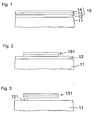
- a sacrificial layer 12 is applied to a substrate 11.
- the substrate 11 is, for example, a silicon wafer or an SOI substrate.
- the sacrificial layer is deposited, for example, from SiO2 in a thickness of, for example, 1 ⁇ m (see Figure 1).
- a first partial layer 13 is applied to the surface of the sacrificial layer 12.
- a second partial layer 14 is applied to the first partial layer 13.
- the first sub-layer 13 and the second sub-layer 14 together form the layer 15.
- the first sub-layer 13 is deposited, for example, from tungsten, the deposition being carried out in such a way that the first sub-layer 13 is under pressure stress.
- the second sub-layer 14 is also formed, for example, from tungsten, the deposition being carried out in such a way that the second sub-layer is under tensile stress stands. The mechanical stresses in the first sub-layer 13 and the second sub-layer 14 are compensated for, so that the moment of force in the center plane of the layer 15 is zero.
- Layer 15 is suitable for producing a self-supporting structure 151 for a micromechanical system.
- the layer 15 is first structured so that the shape of the self-supporting structure 151 in the plane parallel to the surface of the substrate 11 is determined (see FIG. 2).
- a mask and an etching process that is selective with respect to the sacrificial layer 12 are used.
- the sacrificial layer 12 is then selectively etched with respect to the self-supporting structure 151 and to the substrate 11, for example with buffered hydrofluoric acid.
- the sacrificial layer 12 is also partially removed under the self-supporting structure 151, so that it is only firmly connected to the substrate 11 via a support point 121 (see FIG. 3).
- a sacrificial layer 22 is applied to a substrate 21 (see FIG. 4).
- the substrate 21 is, for example, a silicon wafer or an SOI substrate.
- the sacrificial layer 22 is applied, for example, from SiO2 in a thickness of, for example, 1 ⁇ m.
- a first partial layer 23 is applied to the sacrificial layer 22.
- An auxiliary layer 24 is applied to the first sub-layer 23.
- a second sub-layer 25 is applied to the auxiliary layer 24.
- An auxiliary layer 26 is applied to the second sub-layer 25.
- a third sub-layer 27 is applied to the auxiliary layer 26.
- An auxiliary layer 28 is applied to the third sub-layer 27.
- a fourth sub-layer 29 is applied to the auxiliary layer 28.
- the first sub-layer 23, the auxiliary layer 24, the second sub-layer 25, the auxiliary layer 26, the third sub-layer 27, the auxiliary layer 28 and the fourth sub-layer 29 together form a layer 30 with reduced mechanical stresses.
- the first sub-layer 23 is applied, for example, from polycrystalline silicon to the sacrificial layer 22. Subsequently, the auxiliary layer 24 made of SiO2 is produced in a thickness of, for example, 0.1 to 3 nm. The auxiliary layer 24 is generated, for example, by a corresponding waiting time in the atmosphere, an oxidizing cleaning or by oxidation at an elevated temperature.
- the second sub-layer 25 is also produced from polycrystalline silicon. Since the auxiliary layer 24 provides the necessary prerequisites for the nucleation and growth of the second sub-layer 25 as the sacrificial layer 22, the second sub-layer 25 grows up analogously to the first sub-layer 23. The stress gradient in the second sub-layer 25 therefore corresponds to that in the first sub-layer 23.
- the auxiliary layer 26 is also produced in a thickness of about 0.1 to 3 nm from SiO2.
- the third sub-layer 27 is also deposited thereon from polycrystalline silicon, the growth of the third sub-layer 27 corresponding to that of the second sub-layer 25 and the first sub-layer 23.
- the auxiliary layer 28 made of SiO2 is applied in a thickness between 0.1 and 3 nm.
- the fourth sub-layer 29 is also grown from the polycrystalline silicon on the auxiliary layer 28.
- the stress gradients are the same in all sub-layers.
- the first partial layer 23 and the third partial layer 27 are deposited from polycrystalline silicon.
- the second sub-layer 25 and the fourth sub-layer 29 are deposited from amorphous silicon.
- the auxiliary layers 24, 26, 28 are in turn deposited from SiO2 in a thickness between 0.1 and 3 nm.
- polycrystalline silicon is deposited, a pressure stress results in the layer.
- amorphous silicon is deposited, tensile stress results in the resulting layer.
- the auxiliary layers 24, 26, 28 ensure that no epitaxial growth occurs when silicon is grown. By tempering the layer 30, the second sub-layer 25 and the fourth sub-layer 29 made of amorphous silicon are converted into polycrystalline silicon.
- dopant is introduced into the partial layers 23, 25, 27, 29. This can take place both after the deposition of the corresponding sub-layer and after the completion of the entire layer 30. So that the layer 30 has a sheet resistance corresponding to a single polysilicon layer of the same thickness, it is advantageous to break the auxiliary layers 24, 26, 28 out of SiO 2 by annealing.
- Such tempering is for example ROA annealing at around 1000 ° C. Such tempering is process compatible.
- Layer 30 is suitable for producing a self-supporting structure in a micromechanical system.
- layer 30 is structured so that a self-supporting structure 301 is created. This is done with the aid of a mask technique and an etching selective to the sacrificial layer 22 (see FIG. 5).
- the sacrificial layer 22 is partially removed in an isotropic etching process, for example with buffered hydrofluoric acid, which takes place selectively with respect to the self-supporting structure 301 and the substrate 21, so that only one support point 221 remains from the sacrificial layer 22, via which the self-supporting structure 301 also coexists is connected to the substrate 21 (see FIG. 6).
- Components for control electronics of the micromechanical system can be implemented in the substrate 21 before or after the manufacture of the self-supporting structure 301.
- the first sub-layer 23, the second sub-layer 25, the third sub-layer 27 and the fourth sub-layer 29 are preferably produced in a thickness between 50 nm and 1 ⁇ m.
Landscapes
- Engineering & Computer Science (AREA)
- Chemical & Material Sciences (AREA)
- Analytical Chemistry (AREA)
- Physics & Mathematics (AREA)
- General Physics & Mathematics (AREA)
- Mechanical Engineering (AREA)
- Manufacturing & Machinery (AREA)
- Microelectronics & Electronic Packaging (AREA)
- Pressure Sensors (AREA)
- Micromachines (AREA)
- Recrystallisation Techniques (AREA)
- Formation Of Insulating Films (AREA)
Applications Claiming Priority (2)
| Application Number | Priority Date | Filing Date | Title |
|---|---|---|---|
| DE4400119 | 1994-01-04 | ||
| DE4400119 | 1994-01-04 |
Publications (3)
| Publication Number | Publication Date |
|---|---|
| EP0663692A2 true EP0663692A2 (fr) | 1995-07-19 |
| EP0663692A3 EP0663692A3 (fr) | 1997-03-12 |
| EP0663692B1 EP0663692B1 (fr) | 2000-02-23 |
Family
ID=6507456
Family Applications (1)
| Application Number | Title | Priority Date | Filing Date |
|---|---|---|---|
| EP94120791A Expired - Lifetime EP0663692B1 (fr) | 1994-01-04 | 1994-12-27 | Procédé de fabrication d'une couche à contraintes mécaniques réduites |
Country Status (4)
| Country | Link |
|---|---|
| US (1) | US5753134A (fr) |
| EP (1) | EP0663692B1 (fr) |
| JP (1) | JPH07211709A (fr) |
| DE (1) | DE59409157D1 (fr) |
Cited By (5)
| Publication number | Priority date | Publication date | Assignee | Title |
|---|---|---|---|---|
| EP0758080A1 (fr) * | 1995-08-09 | 1997-02-12 | Siemens Aktiengesellschaft | Dispositif micromécanique avec un diaphragme perforé sans contraintes |
| DE10206711A1 (de) * | 2002-02-18 | 2003-08-28 | Siemens Ag | Mikromechanisches Bauelement |
| WO2007036422A1 (fr) * | 2005-09-27 | 2007-04-05 | Siemens Aktiengesellschaft | Dispositif comprenant une membrane a contraintes compensees |
| EP2075220A3 (fr) * | 2007-12-27 | 2013-09-04 | Robert Bosch GmbH | Element micromécanique avec une gradient de stress réduit |
| DE102017209173A1 (de) * | 2017-05-31 | 2018-12-06 | Robert Bosch Gmbh | Polykristallines Material mit geringer mechanischer Verspannung; Verfahren zum Erzeugen eines polykristallinen Materials |
Families Citing this family (23)
| Publication number | Priority date | Publication date | Assignee | Title |
|---|---|---|---|---|
| US5658698A (en) * | 1994-01-31 | 1997-08-19 | Canon Kabushiki Kaisha | Microstructure, process for manufacturing thereof and devices incorporating the same |
| DE4445177C5 (de) * | 1994-11-22 | 2015-09-17 | Fraunhofer-Gesellschaft zur Förderung der angewandten Forschung e.V. | Verfahren zur Herstellung mikromechanischer Bauelemente mit freistehenden Mikrostrukturen |
| US6479166B1 (en) | 1998-10-06 | 2002-11-12 | Case Western Reserve University | Large area polysilicon films with predetermined stress characteristics and method for producing same |
| US6268068B1 (en) | 1998-10-06 | 2001-07-31 | Case Western Reserve University | Low stress polysilicon film and method for producing same |
| JP2000183346A (ja) | 1998-12-15 | 2000-06-30 | Toshiba Corp | 半導体装置及びその製造方法 |
| FR2789518B1 (fr) * | 1999-02-10 | 2003-06-20 | Commissariat Energie Atomique | Structure multicouche a contraintes internes controlees et procede de realisation d'une telle structure |
| CN1252837C (zh) * | 2000-04-26 | 2006-04-19 | 奥斯兰姆奥普托半导体股份有限两合公司 | 在GaN基板上的发光二极管芯片和用GaN基板上的发光二极管芯片制造发光二极管元件的方法 |
| EP1277240B1 (fr) * | 2000-04-26 | 2015-05-20 | OSRAM Opto Semiconductors GmbH | Procédé de fabrication d'un composant semi-conducteur emetteur de lumière |
| DE10051465A1 (de) * | 2000-10-17 | 2002-05-02 | Osram Opto Semiconductors Gmbh | Verfahren zur Herstellung eines Halbleiterbauelements auf GaN-Basis |
| TWI289944B (en) * | 2000-05-26 | 2007-11-11 | Osram Opto Semiconductors Gmbh | Light-emitting-diode-element with a light-emitting-diode-chip |
| US6632374B1 (en) * | 2000-09-28 | 2003-10-14 | Xerox Corporation | Method for an optical switch on a silicon on insulator substrate |
| US6504643B1 (en) * | 2000-09-28 | 2003-01-07 | Xerox Corporation | Structure for an optical switch on a substrate |
| US6632373B1 (en) * | 2000-09-28 | 2003-10-14 | Xerox Corporation | Method for an optical switch on a substrate |
| DE60116969T2 (de) * | 2000-09-28 | 2006-07-27 | Xerox Corp. | Herstellung einer Spiegelstruktur |
| US20040007733A1 (en) * | 2002-06-26 | 2004-01-15 | Macronix International Co., Ltd. | Floating gate memory cell and forming method |
| US6872972B2 (en) * | 2003-07-16 | 2005-03-29 | Macronix International Co., Ltd. | Method for forming silicon film with changing grain size by thermal process |
| US7470462B2 (en) * | 2004-02-20 | 2008-12-30 | Rochester Institute Of Technology | Method to control residual stress in a film structure and a system thereof |
| JP4929753B2 (ja) * | 2006-02-22 | 2012-05-09 | オムロン株式会社 | 薄膜構造体の形成方法並びに薄膜構造体、振動センサ、圧力センサ及び加速度センサ |
| KR100888145B1 (ko) | 2007-02-22 | 2009-03-13 | 성균관대학교산학협력단 | 무응력 연성회로기판 제조 장치 및 방법 |
| US9068278B2 (en) * | 2008-12-08 | 2015-06-30 | Alta Devices, Inc. | Multiple stack deposition for epitaxial lift off |
| US8846500B2 (en) | 2010-12-13 | 2014-09-30 | Semiconductor Components Industries, Llc | Method of forming a gettering structure having reduced warpage and gettering a semiconductor wafer therewith |
| US10242929B1 (en) * | 2017-11-30 | 2019-03-26 | Semiconductor Components Industries, Llc | Method of forming a multilayer structure for reducing defects in semiconductor devices and structure |
| US12040241B2 (en) * | 2019-12-13 | 2024-07-16 | Xidian University | Package structure for semiconductor device and preparation method thereof |
Family Cites Families (10)
| Publication number | Priority date | Publication date | Assignee | Title |
|---|---|---|---|---|
| US4339303A (en) * | 1981-01-12 | 1982-07-13 | Kollmorgen Technologies Corporation | Radiation stress relieving of sulfone polymer articles |
| JPS63136521A (ja) * | 1986-11-27 | 1988-06-08 | Sharp Corp | X線リソグラフイ−用マスク |
| KR910006741B1 (ko) * | 1988-07-28 | 1991-09-02 | 재단법인 한국전자통신연구소 | 비정질 탄소 지지막을 이용한 x-선 리소그라피 마스크의 제조방법 |
| US5059556A (en) * | 1988-09-28 | 1991-10-22 | Siemens-Bendix Automotive Electronics, L.P. | Low stress polysilicon microstructures |
| GB8921722D0 (en) * | 1989-09-26 | 1989-11-08 | British Telecomm | Micromechanical switch |
| US4980018A (en) * | 1989-11-14 | 1990-12-25 | Intel Corporation | Plasma etching process for refractory metal vias |
| US4980020A (en) * | 1989-12-22 | 1990-12-25 | Texas Instruments Incorporated | Local interconnect etch technique |
| US5154810A (en) * | 1991-01-29 | 1992-10-13 | Optical Coating Laboratory, Inc. | Thin film coating and method |
| JPH05102326A (ja) * | 1991-09-13 | 1993-04-23 | Nec Corp | 半導体装置 |
| US5241864A (en) * | 1992-06-17 | 1993-09-07 | Motorola, Inc. | Double pinned sensor utilizing a tensile film |
-
1994
- 1994-11-23 US US08/347,118 patent/US5753134A/en not_active Expired - Fee Related
- 1994-12-26 JP JP6337240A patent/JPH07211709A/ja active Pending
- 1994-12-27 EP EP94120791A patent/EP0663692B1/fr not_active Expired - Lifetime
- 1994-12-27 DE DE59409157T patent/DE59409157D1/de not_active Expired - Fee Related
Cited By (8)
| Publication number | Priority date | Publication date | Assignee | Title |
|---|---|---|---|---|
| EP0758080A1 (fr) * | 1995-08-09 | 1997-02-12 | Siemens Aktiengesellschaft | Dispositif micromécanique avec un diaphragme perforé sans contraintes |
| DE10206711A1 (de) * | 2002-02-18 | 2003-08-28 | Siemens Ag | Mikromechanisches Bauelement |
| DE10206711B4 (de) * | 2002-02-18 | 2012-02-23 | Siemens Ag | Mikromechanisches Bauelement |
| WO2007036422A1 (fr) * | 2005-09-27 | 2007-04-05 | Siemens Aktiengesellschaft | Dispositif comprenant une membrane a contraintes compensees |
| EP2075220A3 (fr) * | 2007-12-27 | 2013-09-04 | Robert Bosch GmbH | Element micromécanique avec une gradient de stress réduit |
| DE102017209173A1 (de) * | 2017-05-31 | 2018-12-06 | Robert Bosch Gmbh | Polykristallines Material mit geringer mechanischer Verspannung; Verfahren zum Erzeugen eines polykristallinen Materials |
| CN108975262A (zh) * | 2017-05-31 | 2018-12-11 | 罗伯特·博世有限公司 | 具有小的机械张力的多晶材料和用于产生多晶材料的方法 |
| US10766778B2 (en) | 2017-05-31 | 2020-09-08 | Robert Bosch Gmbh | Polycrystalline material having low mechanical strain; method for producing a polycrystalline material |
Also Published As
| Publication number | Publication date |
|---|---|
| EP0663692A3 (fr) | 1997-03-12 |
| JPH07211709A (ja) | 1995-08-11 |
| DE59409157D1 (de) | 2000-03-30 |
| US5753134A (en) | 1998-05-19 |
| EP0663692B1 (fr) | 2000-02-23 |
Similar Documents
| Publication | Publication Date | Title |
|---|---|---|
| EP0663692B1 (fr) | Procédé de fabrication d'une couche à contraintes mécaniques réduites | |
| DE10063991B4 (de) | Verfahren zur Herstellung von mikromechanischen Bauelementen | |
| DE19680590B4 (de) | Verfahren zur Herstellung von Beschleunigungssensoren | |
| DE69218667T2 (de) | Verfahren zur Herstellung von Micromaschinen | |
| EP3526158B1 (fr) | Procédé pour produire un capteur de pression micromécanique découplé de contraintes | |
| WO2007068590A1 (fr) | Composant micromecanique et procede de fabrication dudit composant | |
| DE69709680T2 (de) | Mehrfache örtliche oxidation zur mikrobearbeitung der oberfläche | |
| DE69702745T2 (de) | Methode zur Herstellung von mikromechanischen Drucksensoren | |
| DE4445177C5 (de) | Verfahren zur Herstellung mikromechanischer Bauelemente mit freistehenden Mikrostrukturen | |
| DE10241450A1 (de) | Verfahren zur Herstellung eines Bauteils mit einem Sensorelement, insbesondere eines Verformungssensors | |
| EP1360143B1 (fr) | Procede de realisation de structures superficielles micromecaniques, et capteur | |
| WO2002008711A1 (fr) | Procede de production d'un composant a couche mince, notamment un capteur de haute pression a couche mince et composant a couche mince correspondant | |
| DE102006007729A1 (de) | Verfahren zur Herstellung eines MEMS-Substrats, entsprechendes MEMS-Substrat und MEMS-Prozess unter Verwendung des MEMS-Substrats | |
| DE19839123C1 (de) | Mikromechanische Struktur | |
| EP0793736B1 (fr) | Procede de production de composants micromecaniques a microstructures ou membranes separees | |
| EP1347264B1 (fr) | Procédé de fabrication d'une sonde pour SPM | |
| EP1227061A2 (fr) | Procédé de fabrication d'un dispositif microméchanique | |
| DE4415567B4 (de) | Verfahren zur Erzeugung einer SOI-Struktur mit einer Isolationsschicht auf einem Siliziumwafer und einer darauf epitaktisch aufgebrachten Siliziumschicht | |
| DE19710324A1 (de) | Verfahren zur Herstellung von mikromechanische Strukturen aufweisenden Halbleiterbauelemente | |
| DE102004036433B4 (de) | Mikromechanisches Bauteil und Verfahren zur Herstellung eines solchen Bauteils | |
| EP0883169A2 (fr) | Méthode de fabrication d'un transistor à couches minces | |
| EP0309782B1 (fr) | Procédé d'attache du silicium (100) | |
| EP2075220B1 (fr) | Element micromécanique avec une gradient de stress réduit | |
| DE102018209503A1 (de) | Verfahren zur Herstellung eines MEMS-Drucksensors | |
| DE102005002304B4 (de) | Mikroelektromechanischer Sensor und Verfahren zu dessen Herstellung |
Legal Events
| Date | Code | Title | Description |
|---|---|---|---|
| PUAI | Public reference made under article 153(3) epc to a published international application that has entered the european phase |
Free format text: ORIGINAL CODE: 0009012 |
|
| AK | Designated contracting states |
Kind code of ref document: A2 Designated state(s): DE FR GB IT NL |
|
| PUAL | Search report despatched |
Free format text: ORIGINAL CODE: 0009013 |
|
| AK | Designated contracting states |
Kind code of ref document: A3 Designated state(s): DE FR GB IT NL |
|
| 17P | Request for examination filed |
Effective date: 19970520 |
|
| 17Q | First examination report despatched |
Effective date: 19980403 |
|
| GRAG | Despatch of communication of intention to grant |
Free format text: ORIGINAL CODE: EPIDOS AGRA |
|
| GRAG | Despatch of communication of intention to grant |
Free format text: ORIGINAL CODE: EPIDOS AGRA |
|
| GRAH | Despatch of communication of intention to grant a patent |
Free format text: ORIGINAL CODE: EPIDOS IGRA |
|
| GRAH | Despatch of communication of intention to grant a patent |
Free format text: ORIGINAL CODE: EPIDOS IGRA |
|
| GRAA | (expected) grant |
Free format text: ORIGINAL CODE: 0009210 |
|
| AK | Designated contracting states |
Kind code of ref document: B1 Designated state(s): DE FR GB IT NL |
|
| REF | Corresponds to: |
Ref document number: 59409157 Country of ref document: DE Date of ref document: 20000330 |
|
| ITF | It: translation for a ep patent filed | ||
| ET | Fr: translation filed | ||
| GBT | Gb: translation of ep patent filed (gb section 77(6)(a)/1977) |
Effective date: 20000502 |
|
| PLBE | No opposition filed within time limit |
Free format text: ORIGINAL CODE: 0009261 |
|
| STAA | Information on the status of an ep patent application or granted ep patent |
Free format text: STATUS: NO OPPOSITION FILED WITHIN TIME LIMIT |
|
| 26N | No opposition filed | ||
| PGFP | Annual fee paid to national office [announced via postgrant information from national office to epo] |
Ref country code: NL Payment date: 20010630 Year of fee payment: 7 |
|
| PGFP | Annual fee paid to national office [announced via postgrant information from national office to epo] |
Ref country code: FR Payment date: 20011204 Year of fee payment: 8 |
|
| PGFP | Annual fee paid to national office [announced via postgrant information from national office to epo] |
Ref country code: GB Payment date: 20011206 Year of fee payment: 8 |
|
| REG | Reference to a national code |
Ref country code: GB Ref legal event code: IF02 |
|
| PG25 | Lapsed in a contracting state [announced via postgrant information from national office to epo] |
Ref country code: NL Free format text: LAPSE BECAUSE OF NON-PAYMENT OF DUE FEES Effective date: 20020701 |
|
| NLV4 | Nl: lapsed or anulled due to non-payment of the annual fee |
Effective date: 20020701 |
|
| PG25 | Lapsed in a contracting state [announced via postgrant information from national office to epo] |
Ref country code: GB Free format text: LAPSE BECAUSE OF NON-PAYMENT OF DUE FEES Effective date: 20021227 |
|
| GBPC | Gb: european patent ceased through non-payment of renewal fee |
Effective date: 20021227 |
|
| PG25 | Lapsed in a contracting state [announced via postgrant information from national office to epo] |
Ref country code: FR Free format text: LAPSE BECAUSE OF NON-PAYMENT OF DUE FEES Effective date: 20030901 |
|
| REG | Reference to a national code |
Ref country code: FR Ref legal event code: ST |
|
| PG25 | Lapsed in a contracting state [announced via postgrant information from national office to epo] |
Ref country code: IT Free format text: LAPSE BECAUSE OF NON-PAYMENT OF DUE FEES;WARNING: LAPSES OF ITALIAN PATENTS WITH EFFECTIVE DATE BEFORE 2007 MAY HAVE OCCURRED AT ANY TIME BEFORE 2007. THE CORRECT EFFECTIVE DATE MAY BE DIFFERENT FROM THE ONE RECORDED. Effective date: 20051227 |
|
| PGFP | Annual fee paid to national office [announced via postgrant information from national office to epo] |
Ref country code: DE Payment date: 20070213 Year of fee payment: 13 |
|
| PG25 | Lapsed in a contracting state [announced via postgrant information from national office to epo] |
Ref country code: DE Free format text: LAPSE BECAUSE OF NON-PAYMENT OF DUE FEES Effective date: 20080701 |