EP0664565A2 - Dispositif à jonction supraconducteur-conducteur normal - Google Patents
Dispositif à jonction supraconducteur-conducteur normal Download PDFInfo
- Publication number
- EP0664565A2 EP0664565A2 EP95300423A EP95300423A EP0664565A2 EP 0664565 A2 EP0664565 A2 EP 0664565A2 EP 95300423 A EP95300423 A EP 95300423A EP 95300423 A EP95300423 A EP 95300423A EP 0664565 A2 EP0664565 A2 EP 0664565A2
- Authority
- EP
- European Patent Office
- Prior art keywords
- normal
- region
- energy
- junction device
- superconducting material
- Prior art date
- Legal status (The legal status is an assumption and is not a legal conclusion. Google has not performed a legal analysis and makes no representation as to the accuracy of the status listed.)
- Granted
Links
- 239000004020 conductor Substances 0.000 title claims abstract description 6
- 239000000463 material Substances 0.000 claims abstract description 63
- 239000002800 charge carrier Substances 0.000 claims abstract description 9
- 239000004065 semiconductor Substances 0.000 claims description 22
- 239000002184 metal Substances 0.000 claims description 15
- 229910052751 metal Inorganic materials 0.000 claims description 15
- 239000000969 carrier Substances 0.000 claims 1
- 239000002887 superconductor Substances 0.000 description 21
- 230000005540 biological transmission Effects 0.000 description 8
- 238000010586 diagram Methods 0.000 description 6
- 238000000034 method Methods 0.000 description 6
- 230000004888 barrier function Effects 0.000 description 4
- 230000001747 exhibiting effect Effects 0.000 description 2
- 238000004519 manufacturing process Methods 0.000 description 2
- 230000004048 modification Effects 0.000 description 2
- 238000012986 modification Methods 0.000 description 2
- 239000000758 substrate Substances 0.000 description 2
- 230000001419 dependent effect Effects 0.000 description 1
- 230000000694 effects Effects 0.000 description 1
- 150000002739 metals Chemical class 0.000 description 1
- 230000002123 temporal effect Effects 0.000 description 1
- 239000013598 vector Substances 0.000 description 1
Images


Classifications
-
- H—ELECTRICITY
- H10—SEMICONDUCTOR DEVICES; ELECTRIC SOLID-STATE DEVICES NOT OTHERWISE PROVIDED FOR
- H10D—INORGANIC ELECTRIC SEMICONDUCTOR DEVICES
- H10D64/00—Electrodes of devices having potential barriers
- H10D64/60—Electrodes characterised by their materials
- H10D64/608—Electrodes characterised by their materials being superconducting
Definitions
- This invention relates to a superconductor-normal conductor junction device.
- the Fermi level of the normal material aligns with the centre of the gap 2 ⁇ between the quasiparticle energy E Q and the pair energy E S associated with a superconductor.
- a barrier region exists between the normal and superconducting regions, the height of which depends upon the two materials involved and the fabrication procedures used. In most junctions which have been fabricated hitherto, the barrier is sufficiently high or wide enough that current cannot flow until the magnitude of the applied bias is greater than half the superconductor gap ⁇ , bringing the Fermi level of the normal conducting material E1 in line with either the pair energy E S or the quasiparticle energy E Q .
- Andreev reflection For appropriate material conditions, a different process known as Andreev reflection can occur.
- this process when an electron is incident upon the barrier, from within the normal material, it can propagate into the superconducting material only if it pairs with another electron, usually from the normal side.
- a reflected hole, with reverse group velocity and negative effective mass is formed and travels back along the original electron path.
- two electrons can simultaneously tunnel across the barrier, one from the Fermi energy and one from an energy level as much below the pair energy as the Fermi level is above. This give an excess current, when compared with normal electron transport since pairs of electrons are formed in the superconducting material.
- a review of Andreev reflection is given in A.F. Andreev, Zh, Eksp Teor, Fiz 46, 1823 (1964) [Sov. Phys.-JETP 19, 1228 (1964)].
- a superconductor-normal conductor junction device comprises: a region of superconducting material; a first region of normal material forming a first junction with the superconducting material; and a second region of normal material forming a second junction with the superconducting material.
- the Fermi level of the first region of normal material is so arranged relative to a given energy level in the superconducting material that charge carriers in the first normal material undergo Andreev reflection at the first junction, resulting in pairs of the charge carriers entering said given energy level in the superconducting material, and the Fermi level of the second region of normal material is so arranged relative to said given level in the superconducting material that said charge carriers conduct from the superconducting material through the second region.
- the superconducting material can be used as a contact wire in a semiconductor structure, with the advantage that electrons can be injected into the wire by means of a relatively low applied biases.
- junctions can be used to control current flow and can be arranged to exhibit symmetric or asymmetric negative differential resistance so that the device may itself be used to control the input and output characteristics of the superconducting contact wire.
- the first and/or second normal material may comprise semiconductors or metals.
- a gate may be provided to control characteristics of the device.
- this shows the energy diagram for a normal material-superconductor-normal material sandwich with low transmission junctions.
- Normal material 1 which in this example is metal (but may be a semiconductor) forms a first tunnelling junction J1 with superconductor material 2, which, in turn forms the second junction J2 with normal metal 3.
- E1 and E2 represent the Fermi levels in the normal material regions 1, 3.
- the equilibrium Fermi level E F for the superconductor material 2 is shown as a dotted line.
- the superconducting material exhibits an energy gap 2 ⁇ between energy states between the quasiparticle energy E Q and the pair energy E S .
- Figure la shows the condition of zero bias, in which the Fermi levels E1, E2 of the normal metal regions 1, 3 align with the equilibrium Fermi level E F of the superconductor region 2.
- Figure 1b shows the situation when a small bias is applied.
- the Fermi level E1 of normal material 1 is biased slightly above the equilibrium Fermi level E F for the superconductor 2 and the Fermi level E2 of the normal material 3 is biased slightly downwardly from the Fermi level E F .
- the system is not transmissive.
- the arrows in Figure 1 illustrate the limits of possible Andreev reflection. It will be seen that electron pairs can tunnel from the normal material into the superconducting material 2 but transport from the superconductor into the normal material 3 requires both Andreev reflection and the presence of holes to accept the lower energy electrons which occur in the pairs produced by the reflection.
- FIG. 2a, 2b this shows an arrangement in which relatively high transmission junctions J3, J4 are utilised, fabricated by appropriate selection of materials and fabrication procedures, in a manner known per se for individual junctions. In this case, Andreev reflection can occur at both junctions J3, J4.
- electrodes from each of the metal regions 1, 3 will enter the pair level, charging the superconductor 2 until the pair energy E S matches the Fermi level E1, E2 for each of the metal regions 1, 3.
- Figure 4 illustrates a situation in which the metal region 1 is replaced by a semiconductor 4 having a band gap less than twice the superconductor gap.
- a semiconductor has a conduction band 5, and a valence band 6, separated by band gap 7.
- the semiconductor band gap 7 straddles the pair energy E S symmetrically so that current can again flow with the Andreev reflected hole occurring in the valence band 6 so that electron pairs are produced as shown by arrows A5, A6.
- NDR negative differential resistance
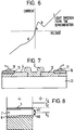
- FIG. 5 A schematic example of a device exhibiting the characteristics of Figure 4b is shown in Figure 5, in which the superconductor 2 is sandwiched between semiconductor 4 and metal contact 3.
- An external connection to the contact 3 is provided by a metallic bond 9, and a diffused ohmic contact 10 provides a connection to the semiconductor 4, with an external connection through metallic bond 11.
- the device exhibits voltage-current characteristic shown in Figure 5, in which region a corresponds to the process described with reference to Figure 4a, region b is a region of NDR corresponding to Figure 4b whereas region c corresponds to the process of Figure 4b, which results in light emission.
- the reverse bias region d corresponds to Figure 4d.
- the metallic region 3 may be replaced by a semiconductor so that under conditions of reverse bias, a negative differential resistance will be exhibited also.
- FIG 7. An example of a device exhibiting NDR for both polarities is shown in Figure 7.
- the superconductor 2 is arranged between semiconductor regions 4, 12, deposited on an insulating substrate 13. External connections to the semiconductor regions 4, 12 are provided by ohmic contacts 15, 16 with associated metallic contacts 17, 18.
- Figure 8 illustrates another modification in which the nature of the Andreev reflections is used to create a non-equilibrium carrier distribution. Only one of the junctions is shown, J3, between p-type semiconductor region 4 and the superconducting material 2.
- the semiconductor has a conduction band 5 and valence band 6, spaced by a band gap 7.
- the pair energy E S is matched to the mid point of the band gap 7 so that Andreev reflection occurs as shown by arrows A7, A8.
- the Andreev reflection depletes both the conduction band and the top of the valence band and as a result, the semiconductor is inverted from an degenerate n-type to a degenerate p-type. This effect can be embodied in device in accordance with the invention.
- all of the described devices can be modified by the provision of a third contact (not shown), capacitively linked to the semiconductor 4, the superconductor 2 or the region 3.
- the resulting gate can be used to control the input or output of the device or hold an offset between the region 3 or 4 and the superconductor 2.
- the invention has application to devices which use high temperature semiconductors, for example to provide superconductor wires on a semiconductor substrate to provide connections between nanofabricated circuit devices, with the advantage that only a very small bias is needed to produce transmission along the superconductor, thus making an on-chip superconducting wire a practical proposition.
- the resulting superconducting wires thus provide high speed interconnects. Also, since the junctions in the device of the invention can themselves provide predetermined non-linear characteristics, the interconnects can contribute to the transfer function for an integrated circuit device.
- the devices can be used in any structures using NDR, and as microwave oscillators.
Landscapes
- Superconductor Devices And Manufacturing Methods Thereof (AREA)
Applications Claiming Priority (2)
| Application Number | Priority Date | Filing Date | Title |
|---|---|---|---|
| GB9401357 | 1994-01-25 | ||
| GB9401357A GB9401357D0 (en) | 1994-01-25 | 1994-01-25 | Semiconductor junctions |
Publications (3)
| Publication Number | Publication Date |
|---|---|
| EP0664565A2 true EP0664565A2 (fr) | 1995-07-26 |
| EP0664565A3 EP0664565A3 (fr) | 1995-09-20 |
| EP0664565B1 EP0664565B1 (fr) | 1998-11-11 |
Family
ID=10749257
Family Applications (1)
| Application Number | Title | Priority Date | Filing Date |
|---|---|---|---|
| EP95300423A Expired - Lifetime EP0664565B1 (fr) | 1994-01-25 | 1995-01-24 | Dispositif à jonction supraconducteur-conducteur normal |
Country Status (4)
| Country | Link |
|---|---|
| US (1) | US6088604A (fr) |
| EP (1) | EP0664565B1 (fr) |
| DE (1) | DE69505853T2 (fr) |
| GB (1) | GB9401357D0 (fr) |
Cited By (1)
| Publication number | Priority date | Publication date | Assignee | Title |
|---|---|---|---|---|
| US6744065B1 (en) | 1997-11-21 | 2004-06-01 | Btg International Limited | Single electron devices |
Families Citing this family (4)
| Publication number | Priority date | Publication date | Assignee | Title |
|---|---|---|---|---|
| US10141493B2 (en) * | 2017-04-11 | 2018-11-27 | Microsoft Technology Licensing, Llc | Thermal management for superconducting interconnects |
| US11645493B2 (en) | 2018-05-04 | 2023-05-09 | Microsoft Technology Licensing, Llc | Flow for quantized neural networks |
| US10453592B1 (en) | 2018-05-07 | 2019-10-22 | Microsoft Technology Licensing Llc | Reducing losses in superconducting cables |
| US11763157B2 (en) | 2019-11-03 | 2023-09-19 | Microsoft Technology Licensing, Llc | Protecting deep learned models |
Family Cites Families (12)
| Publication number | Priority date | Publication date | Assignee | Title |
|---|---|---|---|---|
| US3916432A (en) * | 1974-05-17 | 1975-10-28 | Us Energy | Superconductive microstrip exhibiting negative differential resistivity |
| US4660061A (en) * | 1983-12-19 | 1987-04-21 | Sperry Corporation | Intermediate normal metal layers in superconducting circuitry |
| US4575741A (en) * | 1984-04-26 | 1986-03-11 | International Business Machines Corporation | Cryogenic transistor with a superconducting base and a semiconductor-isolated collector |
| EP0276746B1 (fr) * | 1987-01-30 | 1994-07-13 | Hitachi, Ltd. | Dispositif supraconducteur |
| US4837609A (en) * | 1987-09-09 | 1989-06-06 | American Telephone And Telegraph Company, At&T Bell Laboratories | Semiconductor devices having superconducting interconnects |
| JPH06196767A (ja) * | 1992-12-22 | 1994-07-15 | Hitachi Ltd | 超電導デバイス |
| EP0371426A3 (fr) * | 1988-11-28 | 1990-09-05 | Hitachi, Ltd. | Dispositif supraconducteur |
| EP0413333A3 (en) * | 1989-08-18 | 1991-07-24 | Hitachi, Ltd. | A superconductized semiconductor device |
| JP2616130B2 (ja) * | 1990-04-16 | 1997-06-04 | 日本電気株式会社 | 超伝導素子の製造方法 |
| US5101243A (en) * | 1990-05-21 | 1992-03-31 | International Business Machines Corporation | Superconducting device structures employing anisotropy of the material energy gap |
| US5145832A (en) * | 1991-05-22 | 1992-09-08 | Bell Communications Research, Inc. | Superconducting film on a flexible two-layer zirconia substrate |
| DE69223371T2 (de) * | 1991-09-24 | 1998-06-10 | Sumitomo Electric Industries | Supraleitende Dünnschicht aus oxidisch supraleitendem Material, supraleitender Strompfad und supraleitende Einrichtung mit der supraleitenden Dünnschicht |
-
1994
- 1994-01-25 GB GB9401357A patent/GB9401357D0/en active Pending
-
1995
- 1995-01-19 US US08/375,445 patent/US6088604A/en not_active Expired - Fee Related
- 1995-01-24 EP EP95300423A patent/EP0664565B1/fr not_active Expired - Lifetime
- 1995-01-24 DE DE69505853T patent/DE69505853T2/de not_active Expired - Fee Related
Cited By (1)
| Publication number | Priority date | Publication date | Assignee | Title |
|---|---|---|---|---|
| US6744065B1 (en) | 1997-11-21 | 2004-06-01 | Btg International Limited | Single electron devices |
Also Published As
| Publication number | Publication date |
|---|---|
| DE69505853D1 (de) | 1998-12-17 |
| US6088604A (en) | 2000-07-11 |
| GB9401357D0 (en) | 1994-03-23 |
| EP0664565B1 (fr) | 1998-11-11 |
| EP0664565A3 (fr) | 1995-09-20 |
| DE69505853T2 (de) | 1999-05-27 |
Similar Documents
| Publication | Publication Date | Title |
|---|---|---|
| EP0147482B1 (fr) | Transistor tunnel pour basses températures | |
| EP0828296A2 (fr) | Supraconductivité à haute température dans une jonction contrainte Si/SiGe | |
| US6097036A (en) | Semiconductor logic element and apparatus using thereof | |
| EP0177374A2 (fr) | Dispositif semi-conducteur rapide | |
| EP0160456A2 (fr) | Dispositif supraconducteur | |
| US3250966A (en) | Solid state devices utilizing a metal between two semiconductor materials | |
| EP0664565B1 (fr) | Dispositif à jonction supraconducteur-conducteur normal | |
| JPH03265176A (ja) | 超電導光機能素子 | |
| EP0163031A2 (fr) | Transistor supraconducteur | |
| US3564351A (en) | Supercurrent devices | |
| EP0238406A2 (fr) | Dispositif semi-conducteur à hétérojonction | |
| KR910003836B1 (ko) | 초전도장치 | |
| JPS5823478A (ja) | 電荷結合素子 | |
| US5324976A (en) | Phonon controlled conductivity device | |
| US4994882A (en) | Semiconductor device and method | |
| EP0371426A2 (fr) | Dispositif supraconducteur | |
| JPS61171180A (ja) | 半導体結合超伝導素子 | |
| JP2002076425A (ja) | 光電変換装置 | |
| JPH0577350B2 (fr) | ||
| JPH0411777A (ja) | トリガ素子 | |
| JPH0730160A (ja) | 超伝導トランジスタ | |
| JPH06196767A (ja) | 超電導デバイス | |
| JPH0297921A (ja) | 光変調器 | |
| JPH0431192B2 (fr) | ||
| JPS62222683A (ja) | 超伝導−半導体三端子素子 |
Legal Events
| Date | Code | Title | Description |
|---|---|---|---|
| PUAI | Public reference made under article 153(3) epc to a published international application that has entered the european phase |
Free format text: ORIGINAL CODE: 0009012 |
|
| AK | Designated contracting states |
Kind code of ref document: A2 Designated state(s): DE FR GB NL SE |
|
| PUAL | Search report despatched |
Free format text: ORIGINAL CODE: 0009013 |
|
| AK | Designated contracting states |
Kind code of ref document: A3 Designated state(s): DE FR GB NL SE |
|
| 17P | Request for examination filed |
Effective date: 19960102 |
|
| 17Q | First examination report despatched |
Effective date: 19970714 |
|
| GRAG | Despatch of communication of intention to grant |
Free format text: ORIGINAL CODE: EPIDOS AGRA |
|
| GRAG | Despatch of communication of intention to grant |
Free format text: ORIGINAL CODE: EPIDOS AGRA |
|
| GRAH | Despatch of communication of intention to grant a patent |
Free format text: ORIGINAL CODE: EPIDOS IGRA |
|
| GRAH | Despatch of communication of intention to grant a patent |
Free format text: ORIGINAL CODE: EPIDOS IGRA |
|
| GRAA | (expected) grant |
Free format text: ORIGINAL CODE: 0009210 |
|
| AK | Designated contracting states |
Kind code of ref document: B1 Designated state(s): DE FR GB NL SE |
|
| REF | Corresponds to: |
Ref document number: 69505853 Country of ref document: DE Date of ref document: 19981217 |
|
| ET | Fr: translation filed | ||
| PLBE | No opposition filed within time limit |
Free format text: ORIGINAL CODE: 0009261 |
|
| STAA | Information on the status of an ep patent application or granted ep patent |
Free format text: STATUS: NO OPPOSITION FILED WITHIN TIME LIMIT |
|
| 26N | No opposition filed | ||
| REG | Reference to a national code |
Ref country code: GB Ref legal event code: IF02 |
|
| PGFP | Annual fee paid to national office [announced via postgrant information from national office to epo] |
Ref country code: FR Payment date: 20041203 Year of fee payment: 11 |
|
| PGFP | Annual fee paid to national office [announced via postgrant information from national office to epo] |
Ref country code: GB Payment date: 20050111 Year of fee payment: 11 |
|
| PGFP | Annual fee paid to national office [announced via postgrant information from national office to epo] |
Ref country code: SE Payment date: 20050118 Year of fee payment: 11 |
|
| PGFP | Annual fee paid to national office [announced via postgrant information from national office to epo] |
Ref country code: NL Payment date: 20050127 Year of fee payment: 11 |
|
| PGFP | Annual fee paid to national office [announced via postgrant information from national office to epo] |
Ref country code: DE Payment date: 20050331 Year of fee payment: 11 |
|
| PG25 | Lapsed in a contracting state [announced via postgrant information from national office to epo] |
Ref country code: GB Free format text: LAPSE BECAUSE OF NON-PAYMENT OF DUE FEES Effective date: 20060124 |
|
| PG25 | Lapsed in a contracting state [announced via postgrant information from national office to epo] |
Ref country code: SE Free format text: LAPSE BECAUSE OF NON-PAYMENT OF DUE FEES Effective date: 20060125 |
|
| PG25 | Lapsed in a contracting state [announced via postgrant information from national office to epo] |
Ref country code: FR Free format text: LAPSE BECAUSE OF NON-PAYMENT OF DUE FEES Effective date: 20060131 |
|
| PG25 | Lapsed in a contracting state [announced via postgrant information from national office to epo] |
Ref country code: NL Free format text: LAPSE BECAUSE OF NON-PAYMENT OF DUE FEES Effective date: 20060801 Ref country code: DE Free format text: LAPSE BECAUSE OF NON-PAYMENT OF DUE FEES Effective date: 20060801 |
|
| EUG | Se: european patent has lapsed | ||
| GBPC | Gb: european patent ceased through non-payment of renewal fee |
Effective date: 20060124 |
|
| NLV4 | Nl: lapsed or anulled due to non-payment of the annual fee |
Effective date: 20060801 |
|
| REG | Reference to a national code |
Ref country code: FR Ref legal event code: ST Effective date: 20060929 |