EP0177374A2 - Dispositif semi-conducteur rapide - Google Patents
Dispositif semi-conducteur rapide Download PDFInfo
- Publication number
- EP0177374A2 EP0177374A2 EP85401440A EP85401440A EP0177374A2 EP 0177374 A2 EP0177374 A2 EP 0177374A2 EP 85401440 A EP85401440 A EP 85401440A EP 85401440 A EP85401440 A EP 85401440A EP 0177374 A2 EP0177374 A2 EP 0177374A2
- Authority
- EP
- European Patent Office
- Prior art keywords
- layer
- semiconductor device
- superlattice
- speed semiconductor
- gaas
- Prior art date
- Legal status (The legal status is an assumption and is not a legal conclusion. Google has not performed a legal analysis and makes no representation as to the accuracy of the status listed.)
- Granted
Links
Images


Classifications
-
- H—ELECTRICITY
- H10—SEMICONDUCTOR DEVICES; ELECTRIC SOLID-STATE DEVICES NOT OTHERWISE PROVIDED FOR
- H10D—INORGANIC ELECTRIC SEMICONDUCTOR DEVICES
- H10D48/00—Individual devices not covered by groups H10D1/00 - H10D44/00
- H10D48/30—Devices controlled by electric currents or voltages
- H10D48/32—Devices controlled by only the electric current supplied, or only the electric potential applied, to an electrode which does not carry the current to be rectified, amplified or switched
- H10D48/36—Unipolar devices
- H10D48/362—Unipolar transistors having ohmic electrodes on emitter-like, base-like, and collector-like regions, e.g. hot electron transistors [HET], metal base transistors [MBT], resonant tunnelling transistors [RTT], bulk barrier transistors [BBT], planar doped barrier transistors [PDBT] or charge injection transistors [CHINT]
-
- H—ELECTRICITY
- H10—SEMICONDUCTOR DEVICES; ELECTRIC SOLID-STATE DEVICES NOT OTHERWISE PROVIDED FOR
- H10D—INORGANIC ELECTRIC SEMICONDUCTOR DEVICES
- H10D62/00—Semiconductor bodies, or regions thereof, of devices having potential barriers
- H10D62/80—Semiconductor bodies, or regions thereof, of devices having potential barriers characterised by the materials
- H10D62/81—Semiconductor bodies, or regions thereof, of devices having potential barriers characterised by the materials of structures exhibiting quantum-confinement effects, e.g. single quantum wells; of structures having periodic or quasi-periodic potential variation
- H10D62/815—Semiconductor bodies, or regions thereof, of devices having potential barriers characterised by the materials of structures exhibiting quantum-confinement effects, e.g. single quantum wells; of structures having periodic or quasi-periodic potential variation of structures having periodic or quasi-periodic potential variation, e.g. superlattices or multiple quantum wells [MQW]
- H10D62/8161—Semiconductor bodies, or regions thereof, of devices having potential barriers characterised by the materials of structures exhibiting quantum-confinement effects, e.g. single quantum wells; of structures having periodic or quasi-periodic potential variation of structures having periodic or quasi-periodic potential variation, e.g. superlattices or multiple quantum wells [MQW] potential variation due to variations in composition or crystallinity, e.g. heterojunction superlattices
- H10D62/8162—Semiconductor bodies, or regions thereof, of devices having potential barriers characterised by the materials of structures exhibiting quantum-confinement effects, e.g. single quantum wells; of structures having periodic or quasi-periodic potential variation of structures having periodic or quasi-periodic potential variation, e.g. superlattices or multiple quantum wells [MQW] potential variation due to variations in composition or crystallinity, e.g. heterojunction superlattices having quantum effects only in the vertical direction, i.e. layered structures having quantum effects solely resulting from vertical potential variation
- H10D62/8164—Semiconductor bodies, or regions thereof, of devices having potential barriers characterised by the materials of structures exhibiting quantum-confinement effects, e.g. single quantum wells; of structures having periodic or quasi-periodic potential variation of structures having periodic or quasi-periodic potential variation, e.g. superlattices or multiple quantum wells [MQW] potential variation due to variations in composition or crystallinity, e.g. heterojunction superlattices having quantum effects only in the vertical direction, i.e. layered structures having quantum effects solely resulting from vertical potential variation comprising only semiconductor materials
-
- H—ELECTRICITY
- H10—SEMICONDUCTOR DEVICES; ELECTRIC SOLID-STATE DEVICES NOT OTHERWISE PROVIDED FOR
- H10D—INORGANIC ELECTRIC SEMICONDUCTOR DEVICES
- H10D62/00—Semiconductor bodies, or regions thereof, of devices having potential barriers
- H10D62/80—Semiconductor bodies, or regions thereof, of devices having potential barriers characterised by the materials
- H10D62/82—Heterojunctions
- H10D62/824—Heterojunctions comprising only Group III-V materials heterojunctions, e.g. GaN/AlGaN heterojunctions
Definitions
- the present invention relates to a high-speed semiconductor device, more particularly to a hot electron transistor (HET) device which includes a heterojunction emitter, base, collector, and a superlattice means between the emitter and the base.
- HET hot electron transistor
- a high-speed semiconductor device including: an emitter layer; a base layer; a collector layer; a potential-barrier layer disposed between the base layer and the collector layer; and a superlattice disposed between the emitter layer and the base layer, formed with at least one quantum well therein and having a low impedance state for tunneling carriers therethrough.
- the superlattice includes at least one set of quantum-well forming layer regions having thin potential barrier layers and a thin quantum-well layer between the potential barrier layers, which are formed with a heterojunction structure, and defines the quantum well and the low impedance state.
- the superlattice may include a plurality of sets of quantum-well forming layer regions which are stack-formed with a periodical structure and has at least one conduction mini-energy band for tunneling the carriers therethrough.
- the high-speed semiconductor device may further include a graded layer disposed between the emitter layer and the superlattice and having a conduction-energy level which is approximately equal to that of the emitter layer at one end and is also approximately equal to a predetermined conduction-energy level of the superlattice at another end, for allowing tunneling of the carriers therethrough.
- the carriers in the emitter layer are transported along the graded conduction-energy level in the graded layer, tunneled through the superlattice with the predetermined conduction-energy level and injected into the base layer.
- the high-speed semiconductor device may be given a predetermined DC bias for a resonant tunneling phenomenon of the carriers at the superlattice, thus may output a signal having a 2 to the "n" power multiplied frequency when an input pulse signal having a predetermined'voltage range and predetermined slopes is supplied to the base layer.
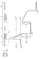
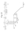
- Figure 1 is a conduction-energy-band diagram of a prior art HET device.
- reference E FE represents a pseudo-Fermi level at an n-type GaAs emitter layer 1
- E FB a pseudo-Fermi level at an n-type GaAs base layer 3
- E BC a pseudo-Fermi level at an n-type GaAs collector layer 5
- AE a conduction-band energy difference between the energy level of the barrier layer 2 and the energy level of the base 3
- ⁇ c a conduction-band discontinuity.
- the application of a higher voltage between the base layer 3 and the emitter layer 1 is required. If a voltage higher than that mentioned above is supplied between the base layer 3 and the emitter layer 1, the gradient of the barrier at the potential barrier layer 2 is changed as shown by the dashed line in Fig. 1 and the energy level of the electrons is increased to ⁇ E C' as shown in Fig. 1. As a result, the number of the electrons injected into the base layer 3 should be increased in principle.
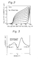
- Figure 3 is a graph of an example of the conduction-energy-band structure of GaAs (See “Physics of Semiconductor Devices” Second Edition, by S.M. Sze, John Wiley & Sons, p 13).
- the energy-band structure includes a so-called L-valley, r-valley, and X-valley.
- L-valley When an electron is at the r-valley, the effective mass thereof is small and the mobility thereof is high.
- the electron is at the X-valley or L-valley, the effective mass thereof is large and the mobility thereof is low. If the energy level of the electrons at the r-valley is lifted as shown in Fig.
- the electrons can be affected by intervalley scattering, that is, the electrons in the r-valley can be transferred to the L- or X-valley by phonons. Due to the intervalley scattering, the electrons injected into the base layer 3 and having a high-energy level can be scattered in a variety of directions, decreasing the number of electrons reaching the collector layer 5. Accordingly, the benefit of increasing the voltage between the emitter layer 1 and the base layer 3 cannot be obtained.
- the current amplification factor a under 77°K is, for example, approximately 0.5 when the base layer is grounded and approximately 1 when the emitter layer is grounded.
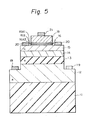
- Figure 4 is a sectional view of a semifinished HET device.
- the HET device consists of a semi-insulating GaAs substrate 11, an n-type GaAs collector contact layer 12, an n-type GaAs collector layer 13, a non-doped impurity Al 0.3 Ga 0.7 As collector- side potential barrier layer 14, an n-type GaAs base layer 15, a superlattice, i.e., emitter-side potential barrier layer 16, and an n -type GaAs emitter layer 18.
- the superlattice consisting of the non-doped impurity AlAs layers 16Al and 16A2 and a non-doped impurity GaAs layer 16B formed between the non-doped impurity AlAs layers 16A1 and 16A2 is disposed between the emitter layer 18 and the base layer 15, instead of the non-doped impurity AlGaAs potential barrier layer 2 in the prior art mentioned above.
- the above construction of the HET device is formed by the MBE process.
- Figure 5 is a sectional view of the HET device shown in Fig. 4.
- the HET device in Fig. 5 is formed from the semifinished HET device as shown in Fig. 4 by the following processes:
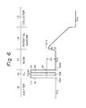
- Figure 6 is a conduction-energy-band diagram of the HET device shown in Fig. 5.
- a so-called GaAs quantum well 7 is formed.
- the heterojunction layer of the extra-thin non-doped, impurity AlAs layers 16Al and 16A2 and the extra-thin non-doped impurity GaAs layer 16B between them the motion of the electrons which move in a direction perpendicular to the heterojunction surface is quantized, with a resultant formation of the quantum well 7.
- the thickness of the above layers 16A1, o o o 16A2, 16B can be 10 A to 100 A, preferably 30 A to 0 50 A.
- “superlattice” has various definitions.
- “superlattice” is defined as a layer (or region) formed with at least one quantum well therein.
- the electrons in the emitter layer 18 are tunneled through the first thin potential barrier wall 81, whereby the electrons reach the quantum well region. Electrons having an energy level equal to a sub-band 91 are further tunneled through the second thin potential barrier wall 82. As a result, the hot electrons e are injected into the base layer 15.
- the above sub-band 91 defines an energy level Ee of the hot electrons in the base layer 15.
- Each sub-band may provide a low impedance state, because the sub-band may trap electrons having an energy equal to the sub-band, which are injected into the base layer 15 tunneling through the second thin barrier layer 16A2.
- the above energy level Ee of the hot electrons e i.e., the sub-band 91, may be selectively defined by selecting the thickness of the heterojunction layers 16A1, 16B, and 16A2 in the superlattice 16. Note that electrons having the above energy level Ee are not affected by the voltage level applied between the emitter layer 18 and the base layer 15.
- the hot electrons e injected into the base layer 15 are ballistically transported to the collector layer 13 with a high speed and without intervalley scattering.
- the current amplification factor a is increased due to the increase of arrival of hot electrons to the collector layer 13.
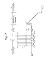
- FIG. 7 is a conduction-energy-band diagram of another embodiment of an HET device in accordance with the present invention.
- the HET device includes a superlattice 16', which consists of non-doped impurity AlAs layers 16Al to 16A4 and non-doped impurity GaAs layers 16Bl to 16B2, each of o which has a thickness of 30 A (3 nm) as mentioned above. That is, the superlattice 16' has a periodical structure of alternatively stacked AlAs layers 16A, which can capture the electrons therein, and GaAs layers 16B, which allow tunneling of the electrons therethrough. In the above heterojunction multilayer superlattice structure, the bond of adjacent quantum wells may be increased, resulting in formation of a mini-energy band 6.
- each sub-band (SBll to SB31) quantum level is degenerated.
- the thickness of the AlAs layers 16A2 and 16A3 between the GaAs layers 16Bl, 16B2, and 16B3 formed with quantum wells QW1 to QW3 therein is extremely thin, and the decrease of electron waves in the AlAs layers is not sufficient.
- the degenerated quantum levels in each sub-band are separated into a plurality of quantum levels forming the mini-energy band 6.
- the electrons may be propagated through the mini-energy band 6, which has an energy band width greater than that of the sub-band.
- mini-energy band 6 The function of the mini-energy band 6 is similar to that of the sub-band 91. However, the mini-energy band 6 enables an increase in the electrons passing through the superlattice 16' rather than the sub-band.
- a current amplification factor a of 0.75 is obtained when the base layer is grounded and of 3 when the emitter is grounded.
- the HET device further includes a non-doped impurity Al x Ga 1-x As graded layer 17, the suffix x designating the composition rate, provided between the emitter layer 18 and the superlattice 16 in addition to the HET device shown in Fig. 5.
- the parameters of the graded layer 17 are as follows:
- the conduction energy bands of the pseudo-Fermi level Ep E at the emitter layer 18 and the sub-band 91 in the superlattice 16 are joined with a gradient.
- the electrons in the emitter layer 18 may easily and surely reach an injection level IL of the superlattice 16, which is equal to the sub-band, along the graded energy level.
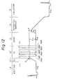
- Figure 11 is a sectional view of a further embodiment of an HET device in accordance with the present invention.
- Figure 12 is a conduction-energy-band diagram of the HET device shown in Fig. 11.
- the concept of provision of the graded layer 17 shown in Fig. 9 may be applied to the HET device including the superlattice 16' having the periodical structure as shown in Fig. 7.
- the HET device shown in Fig. 11 features an improved current amplification factor.
- Figure 13 shows a conduction-energy-band diagram of the resonant tunneling HET device.
- a superlattice 19 consisting of non-doped impurity AlAs layers 19A1 and 19A2 and a non-doped impurity GaAs layer 19B formed similarly to layers 16A1, 16A2, and 16B in Figs. 4 and 5. This corresponds to the superlattice 16 in Figs. 4 and 5.
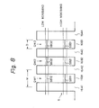
- Figures 14a to 14c show schematically how resonance occurs with an applied DC bias.
- the electrons originate near the Fermi-level E F to the left side of the first barrier of height DE, tunnel into the quantum well, and finally tunnel through the second barrier into unoccupied states.
- Resonance occurs when the electron wave function reflected at the first barrier is cancelled by the wave which is reflected from the second barrier or, equivalently, when the energy of the injected carrier becomes approximately equal to the energy level of the electrons confined in the quantum well.
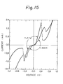
- Figure 15 is a graph showing current-voltage curves for the resonant tunneling structure shown in Figs. 14a to 14c. With the above resonant tunneling phenomenon, a negative resistance having an "n" shape can be observed at a first quadrant of the graph in Fig. 15.
- Figure 16 is a circuit diagram showing an application of the resonant tunneling HET device shown in Fig. 13.
- the resonant tunneling HET device 30 has an emitter E which is grounded and a collector C connected to a resistor 31.
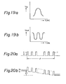
- a pulse signal having predetermined gradients (slopes) over time as shown in Fig. 19a
- two inverted pulses of output signal may be obtained, as shown in Fig. 19b.
- the resonant tunneling HET device acts as a frequency multiplier. The high-speed nature of the HET device is naturally maintained.
- the resonant tunneling HET device having an n-periodical structure superlattice may act as a 2 n- frequency multiplier.
- the HET device may be formed with any combination of the following materials:
- the base layer 15 can be a metal layer e.g. aluminum. All the barrier layers 16A need not be the same material, that is, the same barrier height.
- barrier layers 16A can be an insulating layer, e. g ., A 1 2 0 3 .
- the potential barrier can be formed by a Schottky barrier, which comprises a Schottky junction between a metal base layer Al and a semiconductor collector layer GaAs.
- the base layer 15 can be a p-type doped layer.
- the barrier layer 16A, quantum well layer 16B for the superlattice 16 does not have to be a non-doped semiconductor layer, but may be an n-or p-type doped semiconductor layer.
- the emitter, quantum well, and collector layers are GaAs
- the barrier ) layers 16 A are Al 2 O 3
- the base layer 15 is Al
- the potential barrier layer 14 is the Schottky junction.
Landscapes
- Bipolar Transistors (AREA)
- Junction Field-Effect Transistors (AREA)
Applications Claiming Priority (2)
| Application Number | Priority Date | Filing Date | Title |
|---|---|---|---|
| JP179178/84 | 1984-08-30 | ||
| JP59179178A JPS6158268A (ja) | 1984-08-30 | 1984-08-30 | 高速半導体装置 |
Publications (3)
| Publication Number | Publication Date |
|---|---|
| EP0177374A2 true EP0177374A2 (fr) | 1986-04-09 |
| EP0177374A3 EP0177374A3 (en) | 1987-11-25 |
| EP0177374B1 EP0177374B1 (fr) | 1992-04-15 |
Family
ID=16061296
Family Applications (1)
| Application Number | Title | Priority Date | Filing Date |
|---|---|---|---|
| EP85401440A Expired EP0177374B1 (fr) | 1984-08-30 | 1985-07-15 | Dispositif semi-conducteur rapide |
Country Status (4)
| Country | Link |
|---|---|
| US (1) | US4712121A (fr) |
| EP (1) | EP0177374B1 (fr) |
| JP (1) | JPS6158268A (fr) |
| DE (1) | DE3585864D1 (fr) |
Cited By (15)
| Publication number | Priority date | Publication date | Assignee | Title |
|---|---|---|---|---|
| EP0249455A1 (fr) * | 1986-06-11 | 1987-12-16 | Hitachi, Ltd. | Structure semi-conductrice composite ayant une fraction molaire graduelle et son procédé de fabrication |
| WO1988000398A1 (fr) * | 1986-07-01 | 1988-01-14 | Hughes Aircraft Company | Dispositifs a semi-conducteurs a effet tunnel resonant a puits quantique unique |
| FR2604299A1 (fr) * | 1986-09-23 | 1988-03-25 | Palmier Jean Francois | Transistor bipolaire comportant un emetteur multicouche assurant le confinement des trous |
| EP0256759A3 (en) * | 1986-08-04 | 1988-04-06 | Fujitsu Limited | Resonant tunneling semiconductor device |
| US4786957A (en) * | 1986-01-30 | 1988-11-22 | Director-General Of Agency Of Industrial Science And Technology | Negative differential resistance element |
| US4827320A (en) * | 1986-09-19 | 1989-05-02 | University Of Illinois | Semiconductor device with strained InGaAs layer |
| EP0282407A3 (fr) * | 1987-03-10 | 1989-08-23 | Fujitsu Limited | Dispositif semi-conducteur utilisant des puits quantiques multiples |
| AU593086B2 (en) * | 1986-04-05 | 1990-02-01 | Sumitomo Electric Industries, Ltd. | Compound semiconductor device |
| EP0322773A3 (fr) * | 1987-12-26 | 1990-05-16 | Fujitsu Limited | Dispositif à semi-conducteur avec élément semi-métal |
| US4959696A (en) * | 1985-08-23 | 1990-09-25 | Texas Instruments Incorporated | Three terminal tunneling device and method |
| US5017973A (en) * | 1987-12-25 | 1991-05-21 | Hitachi, Ltd. | Resonant tunneling device |
| EP0279587B1 (fr) * | 1987-02-14 | 1993-04-14 | Fujitsu Limited | Circuit comparateur |
| GB2260858A (en) * | 1991-10-02 | 1993-04-28 | Mitsubishi Electric Corp | Transistors with barrier layers |
| DE19824111A1 (de) * | 1998-05-29 | 1999-12-02 | Daimler Chrysler Ag | Resonanz Phasen Transistor mit gegenphasiger Ladungsträgerinjektion |
| CN102646703A (zh) * | 2012-05-07 | 2012-08-22 | 中国电子科技集团公司第五十五研究所 | 单晶InP基化合物半导体材料薄膜的外延结构 |
Families Citing this family (40)
| Publication number | Priority date | Publication date | Assignee | Title |
|---|---|---|---|---|
| US5214297A (en) * | 1984-11-19 | 1993-05-25 | Fujitsu Limited | High-speed semiconductor device |
| JPS61198776A (ja) * | 1985-02-28 | 1986-09-03 | Fujitsu Ltd | ヘテロ接合バイポ−ラトランジスタおよびその製造方法 |
| JPS6284621A (ja) * | 1985-10-09 | 1987-04-18 | Fujitsu Ltd | 3値論理回路 |
| JPS6285464A (ja) * | 1985-10-09 | 1987-04-18 | Agency Of Ind Science & Technol | ホツトエレクトロントランジスタ |
| CA1291224C (fr) * | 1985-10-12 | 1991-10-22 | Naoki Yokoyama | Circuit logique utilisant un transitor a effet tunnel resonant |
| JPS6323357A (ja) * | 1986-06-14 | 1988-01-30 | Agency Of Ind Science & Technol | 半導体記憶装置 |
| JPH0611056B2 (ja) * | 1985-12-03 | 1994-02-09 | 富士通株式会社 | 高速半導体装置 |
| JPS62211948A (ja) * | 1986-03-13 | 1987-09-17 | Fujitsu Ltd | ヘテロ接合半導体装置 |
| JPS62299073A (ja) * | 1986-06-18 | 1987-12-26 | Agency Of Ind Science & Technol | 半導体装置 |
| US4849799A (en) * | 1986-07-31 | 1989-07-18 | American Telephone And Telegraph Company At&T Bell Laboratories | Resonant tunneling transistor |
| EP0257460B1 (fr) * | 1986-08-12 | 1996-04-24 | Canon Kabushiki Kaisha | Générateur de faisceau d'électrons à l'état solide |
| JPH0666519B2 (ja) * | 1986-08-14 | 1994-08-24 | 東京工業大学長 | 超格子構造体 |
| CN1007479B (zh) * | 1986-08-21 | 1990-04-04 | 朱恩均 | 动能调制热电子晶体管 |
| DE3789891D1 (de) * | 1986-10-22 | 1994-06-30 | Fujitsu Ltd | Halbleiterschaltung mit resonantem Tunnelungseffekt. |
| JP2590842B2 (ja) * | 1986-10-29 | 1997-03-12 | ソニー株式会社 | ヘテロ接合型バイポーラトランジスタ |
| US4907196A (en) * | 1987-04-28 | 1990-03-06 | Fujitsu Limited | Semiconductor memory device using resonant-tunneling transistor |
| US4958208A (en) * | 1987-08-12 | 1990-09-18 | Nec Corporation | Bipolar transistor with abrupt potential discontinuity in collector region |
| US4901122A (en) * | 1987-08-14 | 1990-02-13 | Regents Of The University Of Minnesota | Double-base hot carrier transistor |
| JPH0770743B2 (ja) * | 1987-11-10 | 1995-07-31 | 富士通株式会社 | 共鳴トンネリングバリア構造デバイス |
| US4847666A (en) * | 1987-12-17 | 1989-07-11 | General Motors Corporation | Hot electron transistors |
| US4831340A (en) * | 1988-01-11 | 1989-05-16 | Massachusetts Institute Of Technology | Harmonic multiplier using resonant tunneling device |
| US4825269A (en) * | 1988-03-04 | 1989-04-25 | Stanford University | Double heterojunction inversion base transistor |
| JPH01238161A (ja) * | 1988-03-18 | 1989-09-22 | Fujitsu Ltd | 半導体装置及びその製造方法 |
| US5138408A (en) * | 1988-04-15 | 1992-08-11 | Nec Corporation | Resonant tunneling hot carrier transistor |
| JPH0276262A (ja) * | 1988-09-12 | 1990-03-15 | Fujitsu Ltd | 半導体装置 |
| US4999697A (en) * | 1988-09-14 | 1991-03-12 | At&T Bell Laboratories | Sequential-quenching resonant-tunneling transistor |
| US5121181A (en) * | 1989-01-31 | 1992-06-09 | International Business Machines Corporation | Resonant tunneling photodetector for long wavelength applications |
| US5031013A (en) * | 1990-08-13 | 1991-07-09 | The United States Of America As Represented By The Secretary Of The Army | Infrared hot-electron transistor |
| US6201258B1 (en) * | 1990-08-15 | 2001-03-13 | Texas Instruments Incorporated | Hot carrier transistors utilizing quantum well injector for high current gain |
| US5179037A (en) * | 1991-12-24 | 1993-01-12 | Texas Instruments Incorporated | Integration of lateral and vertical quantum well transistors in the same epitaxial stack |
| US5448087A (en) * | 1992-04-30 | 1995-09-05 | Trw Inc. | Heterojunction bipolar transistor with graded base doping |
| US5242843A (en) * | 1992-10-28 | 1993-09-07 | Allied-Signal Inc. | Method for making a heterojunction bipolar transistor with improved high frequency response |
| US5489785A (en) * | 1994-03-11 | 1996-02-06 | Motorola | Band-to-band resonant tunneling transistor |
| US5731752A (en) * | 1996-04-17 | 1998-03-24 | Loral Vought Systems Corporation | Microwave signal frequency multiplier |
| US6281746B1 (en) | 1999-12-16 | 2001-08-28 | Lockheed Martin Corporation | Parametric cavity microwave amplifier |
| US6265934B1 (en) | 1999-12-16 | 2001-07-24 | Lockheed Martin Corporation | Q-switched parametric cavity amplifier |
| US6297716B1 (en) | 1999-12-16 | 2001-10-02 | Lockheed Martin Corporation | Q-switched cavity multiplier |
| WO2009058580A1 (fr) * | 2007-10-31 | 2009-05-07 | Bae Systems Information And Electronic Systems Integration Inc. | Transistor bipolaire à hétérojonction à forte injection |
| GB201418888D0 (en) * | 2014-10-23 | 2014-12-10 | Univ Lancaster | Improvements relating to electronic memory devices |
| JP7407546B2 (ja) * | 2019-09-24 | 2024-01-04 | 株式会社東芝 | 量子カスケードレーザ |
Family Cites Families (6)
| Publication number | Priority date | Publication date | Assignee | Title |
|---|---|---|---|---|
| DE2607940A1 (de) * | 1976-02-27 | 1977-09-08 | Max Planck Gesellschaft | Mehrschichtiges halbleiterbauelement |
| FR2508707A1 (fr) * | 1981-06-26 | 1982-12-31 | Thomson Csf | Transistor balistique a multiples heterojonctions |
| EP0068064A1 (fr) * | 1981-06-30 | 1983-01-05 | International Business Machines Corporation | Circuit semiconducteur avec une triode à effet tunnel fonctionnant par résonance |
| US4616241A (en) * | 1983-03-22 | 1986-10-07 | The United States Of America As Represented By The United States Department Of Energy | Superlattice optical device |
| JPS60175450A (ja) * | 1984-02-22 | 1985-09-09 | Toshiba Corp | ヘテロ接合バイポ−ラ半導体素子 |
| JPS61121358A (ja) * | 1984-11-19 | 1986-06-09 | Fujitsu Ltd | 高速半導体装置 |
-
1984
- 1984-08-30 JP JP59179178A patent/JPS6158268A/ja active Granted
-
1985
- 1985-07-12 US US06/754,416 patent/US4712121A/en not_active Expired - Lifetime
- 1985-07-15 EP EP85401440A patent/EP0177374B1/fr not_active Expired
- 1985-07-15 DE DE8585401440T patent/DE3585864D1/de not_active Expired - Lifetime
Cited By (19)
| Publication number | Priority date | Publication date | Assignee | Title |
|---|---|---|---|---|
| US4959696A (en) * | 1985-08-23 | 1990-09-25 | Texas Instruments Incorporated | Three terminal tunneling device and method |
| US4786957A (en) * | 1986-01-30 | 1988-11-22 | Director-General Of Agency Of Industrial Science And Technology | Negative differential resistance element |
| AU593086B2 (en) * | 1986-04-05 | 1990-02-01 | Sumitomo Electric Industries, Ltd. | Compound semiconductor device |
| EP0249455A1 (fr) * | 1986-06-11 | 1987-12-16 | Hitachi, Ltd. | Structure semi-conductrice composite ayant une fraction molaire graduelle et son procédé de fabrication |
| WO1988000398A1 (fr) * | 1986-07-01 | 1988-01-14 | Hughes Aircraft Company | Dispositifs a semi-conducteurs a effet tunnel resonant a puits quantique unique |
| EP0256759A3 (en) * | 1986-08-04 | 1988-04-06 | Fujitsu Limited | Resonant tunneling semiconductor device |
| US4825264A (en) * | 1986-08-04 | 1989-04-25 | Fujitsu Limited | Resonant tunneling semiconductor device |
| US4827320A (en) * | 1986-09-19 | 1989-05-02 | University Of Illinois | Semiconductor device with strained InGaAs layer |
| FR2604299A1 (fr) * | 1986-09-23 | 1988-03-25 | Palmier Jean Francois | Transistor bipolaire comportant un emetteur multicouche assurant le confinement des trous |
| EP0279587B1 (fr) * | 1987-02-14 | 1993-04-14 | Fujitsu Limited | Circuit comparateur |
| EP0282407A3 (fr) * | 1987-03-10 | 1989-08-23 | Fujitsu Limited | Dispositif semi-conducteur utilisant des puits quantiques multiples |
| US5017973A (en) * | 1987-12-25 | 1991-05-21 | Hitachi, Ltd. | Resonant tunneling device |
| EP0322773A3 (fr) * | 1987-12-26 | 1990-05-16 | Fujitsu Limited | Dispositif à semi-conducteur avec élément semi-métal |
| GB2260858A (en) * | 1991-10-02 | 1993-04-28 | Mitsubishi Electric Corp | Transistors with barrier layers |
| US5389798A (en) * | 1991-10-02 | 1995-02-14 | Mitsubishi Denki Kabushiki Kaisha | High-speed semiconductor device with graded collector barrier |
| GB2260858B (en) * | 1991-10-02 | 1996-06-12 | Mitsubishi Electric Corp | High-speed semiconductor device and production method therefor |
| DE19824111A1 (de) * | 1998-05-29 | 1999-12-02 | Daimler Chrysler Ag | Resonanz Phasen Transistor mit gegenphasiger Ladungsträgerinjektion |
| CN102646703A (zh) * | 2012-05-07 | 2012-08-22 | 中国电子科技集团公司第五十五研究所 | 单晶InP基化合物半导体材料薄膜的外延结构 |
| CN102646703B (zh) * | 2012-05-07 | 2014-12-10 | 中国电子科技集团公司第五十五研究所 | 单晶InP基化合物半导体材料薄膜的外延结构 |
Also Published As
| Publication number | Publication date |
|---|---|
| JPH0421336B2 (fr) | 1992-04-09 |
| US4712121A (en) | 1987-12-08 |
| DE3585864D1 (de) | 1992-05-21 |
| EP0177374A3 (en) | 1987-11-25 |
| EP0177374B1 (fr) | 1992-04-15 |
| JPS6158268A (ja) | 1986-03-25 |
Similar Documents
| Publication | Publication Date | Title |
|---|---|---|
| EP0177374B1 (fr) | Dispositif semi-conducteur rapide | |
| EP0272985B1 (fr) | Dispositif semi-conducteur à courant constant | |
| EP0159273B1 (fr) | Dispositif semi-conducteur | |
| EP1088347B1 (fr) | Transistor à porteur de charge unique et méthode de detection l'utilisant | |
| US5021841A (en) | Semiconductor device with controlled negative differential resistance characteristic | |
| US4727403A (en) | Double heterojunction semiconductor device with injector | |
| US5091759A (en) | Heterostructure field effect transistor | |
| JP2537852B2 (ja) | 高移動度半導体装置 | |
| US4721983A (en) | Three terminal tunneling device | |
| US5196359A (en) | Method of forming heterostructure field effect transistor | |
| Chow et al. | InAs/AlSb/GaSb resonant interband tunneling diodes and Au-on-InAs/AlSb-superlattice Schottky diodes for logic circuits | |
| JPS6313355B2 (fr) | ||
| US5059545A (en) | Three terminal tunneling device and method | |
| KR960000385B1 (ko) | 전계효과트랜지스터 | |
| US4907045A (en) | Resonant-tunneling functional device using multiple negative differential resistances | |
| JPH09219542A (ja) | ハイブリッド電子デバイス、特にジョセフソン・トランジスタ | |
| EP0216155A2 (fr) | Dispositif à effet-tunnel avec trois pôles | |
| EP0136108B1 (fr) | Dispositif semi-conducteur à hétérojonction | |
| US5280182A (en) | Resonant tunneling transistor with barrier layers | |
| US4786957A (en) | Negative differential resistance element | |
| EP0186301A1 (fr) | Dispositif semi-conducteur à grande vitesse | |
| EP0322773B1 (fr) | Dispositif à semi-conducteur avec élément semi-métal | |
| JPH0654786B2 (ja) | ヘテロ接合半導体デバイス | |
| JP2553760B2 (ja) | 高電子移動度トランジスタ | |
| Takayanagi | Semiconductor-coupled Josephson junctions with a submicron split gate electrode |
Legal Events
| Date | Code | Title | Description |
|---|---|---|---|
| PUAI | Public reference made under article 153(3) epc to a published international application that has entered the european phase |
Free format text: ORIGINAL CODE: 0009012 |
|
| AK | Designated contracting states |
Kind code of ref document: A2 Designated state(s): DE FR GB |
|
| PUAL | Search report despatched |
Free format text: ORIGINAL CODE: 0009013 |
|
| AK | Designated contracting states |
Kind code of ref document: A3 Designated state(s): DE FR GB |
|
| 17P | Request for examination filed |
Effective date: 19880108 |
|
| 17Q | First examination report despatched |
Effective date: 19900319 |
|
| GRAA | (expected) grant |
Free format text: ORIGINAL CODE: 0009210 |
|
| AK | Designated contracting states |
Kind code of ref document: B1 Designated state(s): DE FR GB |
|
| REF | Corresponds to: |
Ref document number: 3585864 Country of ref document: DE Date of ref document: 19920521 |
|
| ET | Fr: translation filed | ||
| PLBE | No opposition filed within time limit |
Free format text: ORIGINAL CODE: 0009261 |
|
| STAA | Information on the status of an ep patent application or granted ep patent |
Free format text: STATUS: NO OPPOSITION FILED WITHIN TIME LIMIT |
|
| 26N | No opposition filed | ||
| PGFP | Annual fee paid to national office [announced via postgrant information from national office to epo] |
Ref country code: DE Payment date: 20010709 Year of fee payment: 17 |
|
| PGFP | Annual fee paid to national office [announced via postgrant information from national office to epo] |
Ref country code: GB Payment date: 20010711 Year of fee payment: 17 |
|
| PGFP | Annual fee paid to national office [announced via postgrant information from national office to epo] |
Ref country code: FR Payment date: 20010712 Year of fee payment: 17 |
|
| REG | Reference to a national code |
Ref country code: GB Ref legal event code: IF02 |
|
| PG25 | Lapsed in a contracting state [announced via postgrant information from national office to epo] |
Ref country code: GB Free format text: LAPSE BECAUSE OF NON-PAYMENT OF DUE FEES Effective date: 20020715 |
|
| PG25 | Lapsed in a contracting state [announced via postgrant information from national office to epo] |
Ref country code: DE Free format text: LAPSE BECAUSE OF NON-PAYMENT OF DUE FEES Effective date: 20030201 |
|
| GBPC | Gb: european patent ceased through non-payment of renewal fee |
Effective date: 20020715 |
|
| PG25 | Lapsed in a contracting state [announced via postgrant information from national office to epo] |
Ref country code: FR Free format text: LAPSE BECAUSE OF NON-PAYMENT OF DUE FEES Effective date: 20030331 |
|
| REG | Reference to a national code |
Ref country code: FR Ref legal event code: ST |