EP0666541B1 - Vorrichtung und Verfahren um Chips mit grösserer Geschwindigkeit als die des Buses synchron zu betreiben - Google Patents
Vorrichtung und Verfahren um Chips mit grösserer Geschwindigkeit als die des Buses synchron zu betreiben Download PDFInfo
- Publication number
- EP0666541B1 EP0666541B1 EP95300657A EP95300657A EP0666541B1 EP 0666541 B1 EP0666541 B1 EP 0666541B1 EP 95300657 A EP95300657 A EP 95300657A EP 95300657 A EP95300657 A EP 95300657A EP 0666541 B1 EP0666541 B1 EP 0666541B1
- Authority
- EP
- European Patent Office
- Prior art keywords
- bus
- chip
- data
- clock signal
- latch
- Prior art date
- Legal status (The legal status is an assumption and is not a legal conclusion. Google has not performed a legal analysis and makes no representation as to the accuracy of the status listed.)
- Expired - Lifetime
Links
Images


Classifications
-
- G—PHYSICS
- G06—COMPUTING OR CALCULATING; COUNTING
- G06F—ELECTRIC DIGITAL DATA PROCESSING
- G06F1/00—Details not covered by groups G06F3/00 - G06F13/00 and G06F21/00
- G06F1/04—Generating or distributing clock signals or signals derived directly therefrom
- G06F1/06—Clock generators producing several clock signals
-
- G—PHYSICS
- G06—COMPUTING OR CALCULATING; COUNTING
- G06F—ELECTRIC DIGITAL DATA PROCESSING
- G06F13/00—Interconnection of, or transfer of information or other signals between, memories, input/output devices or central processing units
- G06F13/38—Information transfer, e.g. on bus
- G06F13/42—Bus transfer protocol, e.g. handshake; Synchronisation
- G06F13/4204—Bus transfer protocol, e.g. handshake; Synchronisation on a parallel bus
- G06F13/4208—Bus transfer protocol, e.g. handshake; Synchronisation on a parallel bus being a system bus, e.g. VME bus, Futurebus, Multibus
- G06F13/4217—Bus transfer protocol, e.g. handshake; Synchronisation on a parallel bus being a system bus, e.g. VME bus, Futurebus, Multibus with synchronous protocol
Definitions
- the present invention relates to electronic circuits constructed from a plurality of chips or circuit blocks connected to a bus, and more particularly, to an improved method of synchronizing the chips to the bus clock.
- the chips are capable of running at significantly higher clock speeds than the bus can support.
- the internal speed of a chip is limited by the length of conductors in the chip and by the various parasitic capacitances in the chip. Since signal propagation distances in a chip are much smaller than the signal propagation distances on the bus, chips can often run at much higher speeds than the bus. If the chips do not need to transfer data to or from the bus on each bus cycle, a significant speed advantage may be obtained by running the chips at a clock speed that exceeds the bus clock.
- EP-A-0478132 discloses a multiple-clocked synchronous processor unit comprising a first processor section working at a higher frequency and having a main bus, and a second processor section having a second bus and working at a lower frequency in which the ratio of the frequencies is 3 to 2.
- the disclosure of this document corresponds generally to the introductory part of the independent claims.
- a data communication system for communicating data between a bus running at a first clock frequency and a circuit block operating synchronously with said data bus at a second clock frequency
- said communication system comprising: clock generation means for generating a bus clock signal at said first clock frequency and a chip clock signal at said second clock frequency wherein said first and second clock signal frequencies are in the ratio of (N-1):N where N is an integer greater than I and wherein said bus and chip clock signals are synchronized once every N cycles of said chip clock signal; means, connected to said circuit block, for receiving data from said bus; means, connected to said circuit block, for transmitting data on said bus; means for generating a synchronization signal indicating said chip clock signal cycle in which said bus and chip clock signals are synchronized; means, connected to said circuit block, for identifying a chip clock signal cycle in which data cannot be transmitted by said circuit block on said bus, one said chip clock signal cycle being present in each contiguous block of N said chip clock cycles, and means, connected to
- a method of synchronizing a chip to a bus comprising the steps of generating a bus clock signal at a first clock frequency and a chip clock signal at a second clock frequency wherein said first and second clock signal frequencies are in the ratio of (N-1):N where N is an integer greater than I and wherein said bus and chip clock signals are synchronized once every N cycles of said chip clock signal, generating a synchronization signal indicating the chip clock signal cycle in which the bus and chip clock signals are synchronized, identifying a chip clock cycle signal in which data cannot be transmitted by the chip on said bus, one such chip clock signal cycle being present in each contiguous block of N chip clock cycles, and identifying a chip clock signal cycle in which no new data can be received from the bus, while such chip clock signal cycle being present in each contiguous block of N chip clock cycles.
- Figure I is a block diagram of a chip utilizing the present invention and which is connected to a synchronous bus.
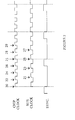
- Figure 2 illustrates the relationship between the chip and bus clocks for the case in which the respective clock frequencies are in the ratio of 4:3.
- Figure 3 is a block diagram of a first interface circuit according to the present invention for transmitting and receiving data from the bus shown in Figure 1.
- Figure 4 is a block diagram of a second interface circuit according to the present invention for transmitting and receiving data from the bus shown in Figure 1.
- FIG. 1 is a block diagram of a chip 15 connected to a synchronous bus 11.
- Chip 15 operates at a frequency set by a chip clock.
- Bus 11 operates at a frequency set by a bus clock which, in general, has a frequency less than that of the chip clock.
- Both the chip and bus clocks are derived from a single clock crystal in clock generator 12.
- the chip clock frequency is related to the bus clock frequency in the ratio of N:(N-1), where N is an integer greater than 1. That is, the possible chip clock to bus clock frequencies are 2:1, 3:2, 4:3, and so on.
- chip 15 receives and transmits data based on the bus clock.
- data is transferred between the bus and the chip via an interface circuit 14 which moves data between the bus domain and the chip domain. The manner in which this interface circuit operates will be discussed in more detail below.
- the present invention is based on the observation that the chip cycles in which data cannot be read or written between the chip and the bus are independent of the value of N if the clocks are in the ratio of N:(N-1).
- Figure 2 illustrates the relationship between the chip and bus clocks for the case in which the respective clock frequencies are in the ratio of 4:3.
- the clock pulses occur in repetitive groups corresponding to 4 chip clock pulse for each 3 bus clock pulses. Once every 4 chip clock pulses, the two clocks will have coincident rising edges as shown by the broken lines. It will be assumed in the following discussion that data is clocked into latches and registers on the rising edges of the respective clock pulses.
- chip 15 receives a synchronization signal that is generated by clock generator 12.
- the synchronization signal informs the synchronization processing circuitry 16 of the chip cycle at which synchronization takes place.
- the synchronization signal can be sent a predetermined number of chip clock cycles before synchrony occurs.
- Synchronization processing circuitry 16 preferably generates send and receive inhibit signals that prevent the other circuitry 13 on the chip from attempting to receive or transmit data during the forbidden receive and transmit time slots.
- Interface circuit 14 depends on the maximum value of N.
- N is less than or equal to 4
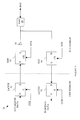
- FIG. 3 is a block diagram of an interface circuit 30 according to the present invention.
- Interface circuit 30 can be divided into two domains, a chip domain which operates in synchrony with the chip clock whose signal is denoted by CCK and a bus domain that is controlled by the bus clock whose signal is denoted by UCK.
- a pad 36 on the chip is used to make the physical connection to the bus.
- Out-bound data is placed in a transparent latch 31.
- the data is read from latch 31 into an edge triggered D register 33 which is preferably an edge triggered flip-flop that is controlled by the bus clock signal.
- a buffer 35 is used to drive the bus line off of the output of register 33.
- in-bound data from the bus is read into a D register 34 which is preferably an edge triggered flip-flop that is controlled by the bus clock.
- the data is transferred to the chip domain via a transparent latch 32 operating off of the chip clock.
- N>4 preferably utilize the interface circuit shown in Figure 4 at 40.
- the chip domain in which the data originates will be referred to as the sender
- the chip domain to which the data is to be transferred will be referred to as the receiver.
- the basic mechanism by which synchronization is achieved involves gating the clock of the sender with a locally generated synchronization signal such that whenever the receiver's latch is updating, the output of the sender's latch remains steady.
- the sender's latch only updates when the receiver's latch is not updating.
- both the sender's latch and the receiver's latch are allowed to update simultaneously. This assures that the receiver's data will always be stable and will be in step with the data the sender intends to transfer.
- register 34 shown in Figure 3 is split into a pair of transparent latches 51 and 52.
- Control circuitry 55 assumes that latch 51's data is captured by latch 42 before new data from latch 52 is received.
- Control circuit 55 includes a control flip-flop which is set low at the falling edge of the sender's clock if and only if a signal referred to as NRSYNC is high.
- the control flip-flop is cleared HIGH unconditionally on the falling edge of the receiver's clock.
- the control flip-flop is also cleared HIGH when NRSYNC is low. Since, as explained in more detail below, NRSYNC will be low when the clock edges from the two frequency domains are coincident, the control flip-flop will allow simultaneous update of sender and receiver domain latches when a concurrent clock edge occurs. When the edges are not coincident, the control flip-flop guarantees that the receiver domain latch has completed updating (i.e., its clock edge has fallen) before the sender domain latch updates its contents.
- control circuit 56 assures that register 43 has clocked out its data before loading new data from latch 41.
- the control circuits utilize signals NDSYNC and NRSYNC which are generated from a single USYNC which informs the chip when coincident rising edges of CCK and UCK will occur.
- NDSYNC is asserted low from the rising edge of CCK from one cycle before the coincident edge of CCK and UCK to the rising edge of CCK one cycle after the coincident edge of CCK and UCK.
- NRSYNC is asserted low from the falling edge of CCK from one half cycle before the coincident rising edge of CCK and UCK to the second falling edge of CCK after the coincident edge of CCK and UCK.
- each chip could detect the synchronization point by comparing the chip and bus clock signals received by the chip. This approach; however, would require this circuitry to be duplicated in each chip. The cost of the additional circuitry makes this approach less attractive.
Landscapes
- Engineering & Computer Science (AREA)
- Theoretical Computer Science (AREA)
- Physics & Mathematics (AREA)
- General Engineering & Computer Science (AREA)
- General Physics & Mathematics (AREA)
- Information Transfer Systems (AREA)
Claims (6)
- Ein Datenkommunikationssystem zum Übermitteln von Daten zwischen einem Bus (11), der bei einer ersten Taktfrequenz läuft, und einem Schaltungsblock (15), der synchron mit dem Datenbus (11) bei einer zweiten Taktfrequenz arbeitet, wobei das Kommunikationssystem folgende Merkmale aufweist: eine Takterzeugungseinrichtung (12) zum Erzeugen eines Bustaktsignals bei der ersten Taktfrequenz und eines Chiptaktsignals bei der zweiten Taktfrequenz, wobei sich die erste und die zweite Taktsignalfrequenz in dem Verhältnis von (N-1):N befinden, wobei N eine Ganzzahl und größer als 1 ist, und wobei das Bustaktsignal und das Chiptaktsignal einmal alle N Zyklen des Chiptaktsignals synchronisiert sind; eine Einrichtung (14), die mit dem Schaltungsblock (15) verbunden ist, zum Empfangen von Daten von dem Bus (11); eine Einrichtung (14), die mit dem Schaltungsblock (15) verbunden ist, zum Übertragen von Daten auf den Bus (11); und eine Einrichtung (12) zum Erzeugen eines Synchronisationssignals, das den Chiptaktsignalzyklus anzeigt, bei dem das Bustaktsignal und das Chiptaktsignal synchronisiert sind; dadurch gekennzeichnet, daß ferner eine Einrichtung (16), die mit dem Schaltungsblock (15) verbunden ist, zum Identifizieren eines Chiptaktsignalzyklus, bei dem keine Daten von dem Schaltungsblock (15) auf den Bus (11) übertragen werden können, wobei ein solcher Chiptaktsignalzyklus in jedem zusammenhängenden Block von N Chiptaktzyklen vorhanden ist, und eine Einrichtung vorgesehen ist, die mit dem Schaltungsblock (15) verbunden ist, zum Identifizieren eines Chiptaktsignalzyklus, bei dem keine neuen Daten von dem Bus (11) empfangen werden können, wobei ein solcher Chiptaktzyklus in jedem zusammenhängenden Block von N Chiptaktzyklen vorhanden ist.
- Das Datenkommunikationssystem gemäß Anspruch 1, bei dem die Empfangseinrichtung folgende Merkmale aufweist: ein erstes Register (34), das verbunden ist, um Daten von dem Bus (11) zu empfangen, wobei das erste Register mit dem Bustaktsignal synchronisiert ist; und eine Latch-Schaltung (32), die mit dem Chiptaktsignal synchronisiert ist.
- Das Datenkommunikationssystem gemäß Anspruch 2, bei dem das erste Register folgende Merkmale aufweist: eine erste Latch-Schaltung (52), das als Antwort auf das Bustaktsignal Daten von dem Bus (11) liest; und eine zweite Latch-Schaltung (51) in Serie mit der ersten Latch-Schaltung, wobei die zweite Latch-Schaltung (51) als Antwort auf ein Übertragungssignal Daten von der ersten Latch-Schaltung (52) empfängt, derart, daß verhindert wird, daß die zweite Latch-Schaltung (51) eine Aktualisierung durchführt, während sich der Zustand der ersten Latch-Schaltung (52) ändert.
- Das Datenkommunikationssystem gemäß einem der vorhergehenden Ansprüche, bei dem die Sendeeinrichtung folgende Merkmale aufweist: eine dritte Latch-Schaltung (31, 41), die mit dem Chiptaktsignal synchronisiert ist und verbunden ist, um Daten von dem Schaltungsblock (15) zu empfangen; und ein zweites Register (33, 43), das verbunden ist, um Daten auf den Bus (11) zu übertragen, wobei das zweite Register (33, 43) mit dem Bustaktsignal synchronisiert ist und mit dem Ausgang der dritten Latch-Schaltung (31, 41) verbunden ist.
- Das Datenkommunikationssystem gemäß Anspruch 4, das ferner eine Einrichtung (56) aufweist, die mit der dritten Latch-Schaltung (31, 41) verbunden ist, zum Verhindern, daß die dritte Latch-Schaltung eine Aktualisierung durchführt, während sich der Zustand des zweiten Registers (43) ändert.
- Ein Verfahren zum Synchronisieren eines Chips mit einem Bus, mit folgenden Schritten: Erzeugen eines Bustaktsignals bei einer ersten Taktfrequenz und eines Chiptaktsignals bei einer zweiten Taktfrequenz, wobei sich die erste und die zweite Taktsignalfrequenz in dem Verhältnis von (N-1):N befinden, wobei N eine Ganzzahl und größer als 1 ist, und wobei das Bustaktsignal und das Chiptaktsignal einmal alle N Zyklen des Chiptaktsignals synchronisiert sind, und Erzeugen eines Synchronisationssignals, das den Chiptaktsignalzyklus angibt, bei dem das Bustaktsignal und das Chiptaktsignal synchronisiert sind, dadurch gekennzeichnet, daß das Verfahren ferner folgende Schritte aufweist: Identifizieren eines Chiptaktzyklussignals, bei dem keine Daten von dem Chip auf den Bus übertragen werden können, wobei ein solcher Chiptaktsignalzyklus in jedem zusammenhängenden Block von N Chiptaktzyklen vorhanden ist, und Identifizieren eines Chiptaktsignalzyklus, bei dem keine neuen Daten von dem Bus empfangen werden können, wobei ein solcher Chiptaktsignalzyklus in jedem zusammenhängenden Block von N Chiptaktzyklen vorhanden ist.
Applications Claiming Priority (2)
| Application Number | Priority Date | Filing Date | Title |
|---|---|---|---|
| US08/191,865 US5600824A (en) | 1994-02-04 | 1994-02-04 | Clock generating means for generating bus clock and chip clock synchronously having frequency ratio of N-1/N responsive to synchronization signal for inhibiting data transfer |
| US191865 | 1998-11-12 |
Publications (2)
| Publication Number | Publication Date |
|---|---|
| EP0666541A1 EP0666541A1 (de) | 1995-08-09 |
| EP0666541B1 true EP0666541B1 (de) | 1999-06-02 |
Family
ID=22707213
Family Applications (1)
| Application Number | Title | Priority Date | Filing Date |
|---|---|---|---|
| EP95300657A Expired - Lifetime EP0666541B1 (de) | 1994-02-04 | 1995-02-02 | Vorrichtung und Verfahren um Chips mit grösserer Geschwindigkeit als die des Buses synchron zu betreiben |
Country Status (4)
| Country | Link |
|---|---|
| US (2) | US5600824A (de) |
| EP (1) | EP0666541B1 (de) |
| JP (1) | JP3565600B2 (de) |
| DE (1) | DE69509932T2 (de) |
Families Citing this family (49)
| Publication number | Priority date | Publication date | Assignee | Title |
|---|---|---|---|---|
| US5771372A (en) * | 1995-10-03 | 1998-06-23 | International Business Machines Corp. | Apparatus for delaying the output of data onto a system bus |
| US5781765A (en) * | 1995-11-03 | 1998-07-14 | Motorola, Inc. | System for data synchronization between two devices using four time domains |
| US5822571A (en) * | 1996-06-05 | 1998-10-13 | Compaq Computer Corporation | Synchronizing data between devices |
| US5758131A (en) * | 1996-09-11 | 1998-05-26 | Hewlett-Packard Company | Bus adapter for synchronizing communications between two circuits running at different clock rates |
| US5909563A (en) * | 1996-09-25 | 1999-06-01 | Philips Electronics North America Corporation | Computer system including an interface for transferring data between two clock domains |
| US5867694A (en) * | 1996-10-07 | 1999-02-02 | International Business Machines Corporation | Information handling system including apparatus and method for controlling clock signals operating at different frequencies |
| US5835752A (en) * | 1996-10-18 | 1998-11-10 | Samsung Electronics Co. Ltd. | PCI interface synchronization |
| US5956256A (en) * | 1996-11-19 | 1999-09-21 | Unisys Corporation | Method and apparatus for optimizing a circuit design having multi-paths therein |
| US5923193A (en) * | 1996-12-11 | 1999-07-13 | Intel Corporation | Method and apparatus for transferring signals between multiple clock timing domains |
| JP3000961B2 (ja) * | 1997-06-06 | 2000-01-17 | 日本電気株式会社 | 半導体集積回路 |
| US5968180A (en) * | 1997-09-30 | 1999-10-19 | Intel Corporation | Data capture circuit for asynchronous data transfer |
| US6396887B1 (en) | 1997-10-10 | 2002-05-28 | Rambus Incorporated | Apparatus and method for generating a distributed clock signal using gear ratio techniques |
| JP3560793B2 (ja) * | 1997-11-27 | 2004-09-02 | 株式会社東芝 | データ転送方法 |
| US5961649A (en) * | 1997-12-04 | 1999-10-05 | Intel Corporation | Method and apparatus for propagating a signal between synchronous clock domains operating at a non-integer frequency ratio |
| US6385735B1 (en) * | 1997-12-15 | 2002-05-07 | Intel Corporation | Method and apparatus for limiting processor clock frequency |
| US6172937B1 (en) * | 1998-05-13 | 2001-01-09 | Intel Corporation | Multiple synthesizer based timing signal generation scheme |
| US6098139A (en) * | 1998-05-27 | 2000-08-01 | 3Com Corporation | Frequency independent asynchronous clock crossing FIFO |
| US6161188A (en) * | 1998-11-17 | 2000-12-12 | Ip-First, L.L.C. | Microprocessor having fuse control and selection of clock multiplier |
| US6275077B1 (en) | 1999-08-31 | 2001-08-14 | Sun Microsystems, Inc. | Method and apparatus for programmable adjustment of bus driver propagation times |
| US6535945B1 (en) | 1999-08-31 | 2003-03-18 | Sun Microsystems, Inc. | Method and apparatus for programmable adjustment of computer system bus parameters |
| US6499113B1 (en) | 1999-08-31 | 2002-12-24 | Sun Microsystems, Inc. | Method and apparatus for extracting first failure and attendant operating information from computer system devices |
| US6609221B1 (en) | 1999-08-31 | 2003-08-19 | Sun Microsystems, Inc. | Method and apparatus for inducing bus saturation during operational testing of busses using a pattern generator |
| US6473871B1 (en) | 1999-08-31 | 2002-10-29 | Sun Microsystems, Inc. | Method and apparatus for HASS testing of busses under programmable control |
| US6546507B1 (en) | 1999-08-31 | 2003-04-08 | Sun Microsystems, Inc. | Method and apparatus for operational envelope testing of busses to identify halt limits |
| US6502212B1 (en) | 1999-08-31 | 2002-12-31 | Sun Microsystems, Inc. | Method and apparatus for bus parameter optimization using probes of system configurations |
| US6535986B1 (en) | 2000-03-14 | 2003-03-18 | International Business Machines Corporation | Optimizing performance of a clocked system by adjusting clock control settings and clock frequency |
| DE10127424B4 (de) * | 2001-06-06 | 2004-09-02 | Infineon Technologies Ag | Elektronische Schaltung mit asynchroner Taktung von Peripherieeinheiten |
| US6931562B1 (en) | 2001-08-23 | 2005-08-16 | Hewlett-Packard Development Company, L.P. | System and method for transferring data from a higher frequency clock domain to a lower frequency clock domain |
| US6928574B1 (en) | 2001-08-23 | 2005-08-09 | Hewlett-Packard Development Company, L.P. | System and method for transferring data from a lower frequency clock domain to a higher frequency clock domain |
| US6983354B2 (en) * | 2002-05-24 | 2006-01-03 | Micron Technology, Inc. | Memory device sequencer and method supporting multiple memory device clock speeds |
| US20040193931A1 (en) * | 2003-03-26 | 2004-09-30 | Akkerman Ryan L. | System and method for transferring data from a first clock domain to a second clock domain |
| US7434084B1 (en) * | 2005-03-10 | 2008-10-07 | Cisco Technology, Inc. | Method and apparatus for eliminating sampling errors on a serial bus |
| US7464284B2 (en) * | 2005-03-22 | 2008-12-09 | Hewlett-Packard Development Company, L.P. | Systems and methods for driving data over a bus where the systems employ a bus clock that is derived from a system clock and a data clock designed to lead the bus clock |
| US7515666B2 (en) * | 2005-07-29 | 2009-04-07 | International Business Machines Corporation | Method for dynamically changing the frequency of clock signals |
| US8671380B2 (en) * | 2011-07-18 | 2014-03-11 | Apple Inc. | Dynamic frequency control using coarse clock gating |
| US9727306B2 (en) | 2014-10-07 | 2017-08-08 | Stmicroelectronics S.R.L. | Bi-synchronous electronic device with burst indicator and related methods |
| US11128742B2 (en) | 2019-03-08 | 2021-09-21 | Microsemi Storage Solutions, Inc. | Method for adapting a constant bit rate client signal into the path layer of a telecom signal |
| US10972084B1 (en) | 2019-12-12 | 2021-04-06 | Microchip Technology Inc. | Circuit and methods for transferring a phase value between circuits clocked by non-synchronous clock signals |
| US11323123B2 (en) | 2019-12-20 | 2022-05-03 | Microchip Technology Inc. | Circuit to correct phase interpolator rollover integral non-linearity errors |
| US10917097B1 (en) | 2019-12-24 | 2021-02-09 | Microsemi Semiconductor Ulc | Circuits and methods for transferring two differentially encoded client clock domains over a third carrier clock domain between integrated circuits |
| US11239933B2 (en) | 2020-01-28 | 2022-02-01 | Microsemi Semiconductor Ulc | Systems and methods for transporting constant bit rate client signals over a packet transport network |
| US11424902B2 (en) | 2020-07-22 | 2022-08-23 | Microchip Technology Inc. | System and method for synchronizing nodes in a network device |
| US11838111B2 (en) | 2021-06-30 | 2023-12-05 | Microchip Technology Inc. | System and method for performing rate adaptation of constant bit rate (CBR) client data with a variable number of idle blocks for transmission over a metro transport network (MTN) |
| US11916662B2 (en) | 2021-06-30 | 2024-02-27 | Microchip Technology Inc. | System and method for performing rate adaptation of constant bit rate (CBR) client data with a fixed number of idle blocks for transmission over a metro transport network (MTN) |
| US12323334B2 (en) | 2021-06-30 | 2025-06-03 | Microchip Technology Inc. | System and method for performing rate adaptation and multiplexing of constant bit rate (CBR) client data for transmission over a metro transport network (MTN) |
| US11736065B2 (en) | 2021-10-07 | 2023-08-22 | Microchip Technology Inc. | Method and apparatus for conveying clock-related information from a timing device |
| US12192079B2 (en) | 2021-11-23 | 2025-01-07 | Microchip Technology Inc. | Method and apparatus for carrying constant bit rate (CBR) client signals using CBR carrier streams comprising frames |
| US11799626B2 (en) | 2021-11-23 | 2023-10-24 | Microchip Technology Inc. | Method and apparatus for carrying constant bit rate (CBR) client signals |
| US12500822B2 (en) | 2022-04-04 | 2025-12-16 | Microchip Technology Inc. | System and method for rate adaptation of packet-oriented client data for transmission over a metro transport network (MTN) |
Family Cites Families (8)
| Publication number | Priority date | Publication date | Assignee | Title |
|---|---|---|---|---|
| JPS5266346A (en) * | 1975-11-29 | 1977-06-01 | Tokyo Electric Co Ltd | Synch. clock control of microcomputer system |
| DE3162749D1 (en) * | 1980-06-30 | 1984-04-26 | Ibm | Data transfer apparatus |
| EP0375794A1 (de) * | 1988-12-24 | 1990-07-04 | International Business Machines Corporation | Methode zur Synchronisierung von Signalen, die auf verschiedenen Chips mit On-Chip-Taktgebern verschiedener Frequenz erzeugt werden |
| US5235698A (en) * | 1989-09-12 | 1993-08-10 | Acer Incorporated | Bus interface synchronization control system |
| US5309561A (en) * | 1990-09-28 | 1994-05-03 | Tandem Computers Incorporated | Synchronous processor unit with interconnected, separately clocked processor sections which are automatically synchronized for data transfer operations |
| US5381542A (en) * | 1991-07-29 | 1995-01-10 | Unisys Corporation | System for switching between a plurality of clock sources upon detection of phase alignment thereof and disabling all other clock sources |
| US5379408A (en) * | 1991-11-08 | 1995-01-03 | Texas Instruments Incorporated | Color palette timing and control with circuitry for producing an additional clock cycle during a clock disabled time period |
| US5347559A (en) * | 1992-12-30 | 1994-09-13 | Digital Equipment Corporation | Apparatus and method of data transfer between systems using different clocks |
-
1994
- 1994-02-04 US US08/191,865 patent/US5600824A/en not_active Expired - Lifetime
-
1995
- 1995-01-31 JP JP01447595A patent/JP3565600B2/ja not_active Expired - Fee Related
- 1995-02-02 DE DE69509932T patent/DE69509932T2/de not_active Expired - Lifetime
- 1995-02-02 EP EP95300657A patent/EP0666541B1/de not_active Expired - Lifetime
-
1996
- 1996-11-07 US US08/744,387 patent/US5708801A/en not_active Expired - Lifetime
Also Published As
| Publication number | Publication date |
|---|---|
| US5600824A (en) | 1997-02-04 |
| EP0666541A1 (de) | 1995-08-09 |
| US5708801A (en) | 1998-01-13 |
| JP3565600B2 (ja) | 2004-09-15 |
| DE69509932D1 (de) | 1999-07-08 |
| DE69509932T2 (de) | 1999-09-30 |
| JPH07253947A (ja) | 1995-10-03 |
Similar Documents
| Publication | Publication Date | Title |
|---|---|---|
| EP0666541B1 (de) | Vorrichtung und Verfahren um Chips mit grösserer Geschwindigkeit als die des Buses synchron zu betreiben | |
| EP0135879B1 (de) | Interface-Schaltung und Verfahren zum Verbinden einer Speichersteuereinrichtung mit einem synchronen oder asynchronen Bussystem | |
| KR101089153B1 (ko) | 상이한 클록 도메인 간에서의 데이터 신호 전송 방법 및 집적 회로 | |
| JP2711035B2 (ja) | マルチクロック同期プロセッサユニット | |
| US6424688B1 (en) | Method to transfer data in a system with multiple clock domains using clock skipping techniques | |
| US5535377A (en) | Method and apparatus for low latency synchronization of signals having different clock speeds | |
| US5070443A (en) | Apparatus for write handshake in high-speed asynchronous bus interface | |
| EP0453199A2 (de) | Rechnersystem mit synchronem Bus | |
| US4835728A (en) | Deterministic clock control apparatus for a data processing system | |
| JP2004506974A (ja) | 複数クロックシステムにおいてスキップパターンを同期させ、クロック送りインターフェイスを初期設定するためのシステムおよび方法 | |
| EP0645717A1 (de) | System und Verfahren für Datensynchronisierung | |
| EP0379772B1 (de) | Programmierbare Zeitsteuerung der Datenübertragung | |
| US5291529A (en) | Handshake synchronization system | |
| US5535343A (en) | Method and apparatus for generating write signals | |
| US5758131A (en) | Bus adapter for synchronizing communications between two circuits running at different clock rates | |
| EP0375794A1 (de) | Methode zur Synchronisierung von Signalen, die auf verschiedenen Chips mit On-Chip-Taktgebern verschiedener Frequenz erzeugt werden | |
| EP0411759B1 (de) | Synchronisiereinrichtung, welche Taktphasenextrapolation verwendet | |
| US4823365A (en) | Synchronization method and elastic buffer circuit | |
| US7333516B1 (en) | Interface for synchronous data transfer between domains clocked at different frequencies | |
| US6760392B1 (en) | Method and apparatus to provide fixed latency early response in a system with multiple clock domains with fixable clock ratios | |
| US6651127B2 (en) | Method of detecting termination of a bus transfer operation | |
| US6041418A (en) | Race free and technology independent flag generating circuitry associated with two asynchronous clocks | |
| JPS62168415A (ja) | ラツチ間伝送方式 | |
| EP0344736A2 (de) | Synchrones Datenübertragungssystem mit grosser Geschwindigkeit | |
| US7170817B2 (en) | Access of two synchronous busses with asynchronous clocks to a synchronous single port ram |
Legal Events
| Date | Code | Title | Description |
|---|---|---|---|
| PUAI | Public reference made under article 153(3) epc to a published international application that has entered the european phase |
Free format text: ORIGINAL CODE: 0009012 |
|
| AK | Designated contracting states |
Kind code of ref document: A1 Designated state(s): DE FR GB |
|
| 17P | Request for examination filed |
Effective date: 19951218 |
|
| GRAG | Despatch of communication of intention to grant |
Free format text: ORIGINAL CODE: EPIDOS AGRA |
|
| 17Q | First examination report despatched |
Effective date: 19980914 |
|
| GRAG | Despatch of communication of intention to grant |
Free format text: ORIGINAL CODE: EPIDOS AGRA |
|
| GRAH | Despatch of communication of intention to grant a patent |
Free format text: ORIGINAL CODE: EPIDOS IGRA |
|
| GRAH | Despatch of communication of intention to grant a patent |
Free format text: ORIGINAL CODE: EPIDOS IGRA |
|
| GRAA | (expected) grant |
Free format text: ORIGINAL CODE: 0009210 |
|
| AK | Designated contracting states |
Kind code of ref document: B1 Designated state(s): DE FR GB |
|
| REF | Corresponds to: |
Ref document number: 69509932 Country of ref document: DE Date of ref document: 19990708 |
|
| ET | Fr: translation filed | ||
| PLBE | No opposition filed within time limit |
Free format text: ORIGINAL CODE: 0009261 |
|
| STAA | Information on the status of an ep patent application or granted ep patent |
Free format text: STATUS: NO OPPOSITION FILED WITHIN TIME LIMIT |
|
| 26N | No opposition filed | ||
| REG | Reference to a national code |
Ref country code: GB Ref legal event code: 732E |
|
| REG | Reference to a national code |
Ref country code: FR Ref legal event code: TP |
|
| REG | Reference to a national code |
Ref country code: GB Ref legal event code: IF02 |
|
| PGFP | Annual fee paid to national office [announced via postgrant information from national office to epo] |
Ref country code: GB Payment date: 20090227 Year of fee payment: 15 |
|
| PGFP | Annual fee paid to national office [announced via postgrant information from national office to epo] |
Ref country code: FR Payment date: 20090217 Year of fee payment: 15 |
|
| PGFP | Annual fee paid to national office [announced via postgrant information from national office to epo] |
Ref country code: DE Payment date: 20100226 Year of fee payment: 16 |
|
| GBPC | Gb: european patent ceased through non-payment of renewal fee |
Effective date: 20100202 |
|
| REG | Reference to a national code |
Ref country code: FR Ref legal event code: ST Effective date: 20101029 |
|
| PG25 | Lapsed in a contracting state [announced via postgrant information from national office to epo] |
Ref country code: FR Free format text: LAPSE BECAUSE OF NON-PAYMENT OF DUE FEES Effective date: 20100301 |
|
| PG25 | Lapsed in a contracting state [announced via postgrant information from national office to epo] |
Ref country code: GB Free format text: LAPSE BECAUSE OF NON-PAYMENT OF DUE FEES Effective date: 20100202 |
|
| REG | Reference to a national code |
Ref country code: DE Ref legal event code: R119 Ref document number: 69509932 Country of ref document: DE Effective date: 20110901 |
|
| PG25 | Lapsed in a contracting state [announced via postgrant information from national office to epo] |
Ref country code: DE Free format text: LAPSE BECAUSE OF NON-PAYMENT OF DUE FEES Effective date: 20110901 |