EP0667644A1 - Dispositif semi-conducteur pour enregistrer plusieurs états et procédé de fabrication - Google Patents
Dispositif semi-conducteur pour enregistrer plusieurs états et procédé de fabrication Download PDFInfo
- Publication number
- EP0667644A1 EP0667644A1 EP95101831A EP95101831A EP0667644A1 EP 0667644 A1 EP0667644 A1 EP 0667644A1 EP 95101831 A EP95101831 A EP 95101831A EP 95101831 A EP95101831 A EP 95101831A EP 0667644 A1 EP0667644 A1 EP 0667644A1
- Authority
- EP
- European Patent Office
- Prior art keywords
- channel
- region
- source
- semiconductor substrate
- drain regions
- Prior art date
- Legal status (The legal status is an assumption and is not a legal conclusion. Google has not performed a legal analysis and makes no representation as to the accuracy of the status listed.)
- Granted
Links
- 239000004065 semiconductor Substances 0.000 title claims abstract description 111
- 238000004519 manufacturing process Methods 0.000 title claims description 14
- 239000000758 substrate Substances 0.000 claims abstract description 62
- 238000009792 diffusion process Methods 0.000 claims abstract description 60
- 239000012535 impurity Substances 0.000 claims abstract description 60
- 238000005468 ion implantation Methods 0.000 claims abstract description 15
- 239000011159 matrix material Substances 0.000 claims description 5
- 238000002955 isolation Methods 0.000 abstract 2
- 150000002500 ions Chemical class 0.000 description 14
- 229920002120 photoresistant polymer Polymers 0.000 description 14
- 238000000034 method Methods 0.000 description 8
- XUIMIQQOPSSXEZ-UHFFFAOYSA-N Silicon Chemical compound [Si] XUIMIQQOPSSXEZ-UHFFFAOYSA-N 0.000 description 7
- -1 arsenic ions Chemical class 0.000 description 7
- 229910052710 silicon Inorganic materials 0.000 description 7
- 239000010703 silicon Substances 0.000 description 7
- VYPSYNLAJGMNEJ-UHFFFAOYSA-N Silicium dioxide Chemical compound O=[Si]=O VYPSYNLAJGMNEJ-UHFFFAOYSA-N 0.000 description 6
- 229910052796 boron Inorganic materials 0.000 description 6
- 229910052814 silicon oxide Inorganic materials 0.000 description 6
- 238000002513 implantation Methods 0.000 description 4
- 229910021420 polycrystalline silicon Inorganic materials 0.000 description 4
- 229920005591 polysilicon Polymers 0.000 description 4
- 230000001133 acceleration Effects 0.000 description 3
- 101000635799 Homo sapiens Run domain Beclin-1-interacting and cysteine-rich domain-containing protein Proteins 0.000 description 2
- 102100030852 Run domain Beclin-1-interacting and cysteine-rich domain-containing protein Human genes 0.000 description 2
- 238000005229 chemical vapour deposition Methods 0.000 description 2
- 230000007423 decrease Effects 0.000 description 2
- 238000010586 diagram Methods 0.000 description 2
- 238000010438 heat treatment Methods 0.000 description 2
- 230000003071 parasitic effect Effects 0.000 description 2
- 238000000059 patterning Methods 0.000 description 2
- OAICVXFJPJFONN-UHFFFAOYSA-N Phosphorus Chemical compound [P] OAICVXFJPJFONN-UHFFFAOYSA-N 0.000 description 1
- 229910052785 arsenic Inorganic materials 0.000 description 1
- 238000010420 art technique Methods 0.000 description 1
- 238000007796 conventional method Methods 0.000 description 1
- 239000006185 dispersion Substances 0.000 description 1
- 239000007943 implant Substances 0.000 description 1
- 230000010354 integration Effects 0.000 description 1
- 229910052698 phosphorus Inorganic materials 0.000 description 1
- 239000011574 phosphorus Substances 0.000 description 1
- 238000000206 photolithography Methods 0.000 description 1
- 230000002265 prevention Effects 0.000 description 1
Images






Classifications
-
- G—PHYSICS
- G11—INFORMATION STORAGE
- G11C—STATIC STORES
- G11C16/00—Erasable programmable read-only memories
- G11C16/02—Erasable programmable read-only memories electrically programmable
- G11C16/04—Erasable programmable read-only memories electrically programmable using variable threshold transistors, e.g. FAMOS
- G11C16/0483—Erasable programmable read-only memories electrically programmable using variable threshold transistors, e.g. FAMOS comprising cells having several storage transistors connected in series
-
- G—PHYSICS
- G11—INFORMATION STORAGE
- G11C—STATIC STORES
- G11C11/00—Digital stores characterised by the use of particular electric or magnetic storage elements; Storage elements therefor
- G11C11/56—Digital stores characterised by the use of particular electric or magnetic storage elements; Storage elements therefor using storage elements with more than two stable states represented by steps, e.g. of voltage, current, phase, frequency
- G11C11/5692—Digital stores characterised by the use of particular electric or magnetic storage elements; Storage elements therefor using storage elements with more than two stable states represented by steps, e.g. of voltage, current, phase, frequency read-only digital stores using storage elements with more than two stable states
-
- H—ELECTRICITY
- H10—SEMICONDUCTOR DEVICES; ELECTRIC SOLID-STATE DEVICES NOT OTHERWISE PROVIDED FOR
- H10B—ELECTRONIC MEMORY DEVICES
- H10B20/00—Read-only memory [ROM] devices
Definitions
- the present invention relates to a semiconductor device and its manufacturing method, and more specifically to a semiconductor device provided with a multiple-state ROM (Read Only Memory) for storing multiple-state level data and its manufacturing method.
- a multiple-state ROM Read Only Memory
- a plurality of memory cells composed of MOS transistors are arranged into a matrix pattern; gates of the memory cells are connected to a plurality of word lines extending in the row direction, respectively; and source and drain diffusion regions are connected to a plurality of bit lines extending in the column direction, respectively.
- Fig. 1 is a circuit diagram thereof, in which the memory cells are arranged into a matrix pattern; each of the gates of the memory cells is connected to each of a plurality of word lines W1, W2, ...; and each of the source and drain diffusion regions is connected to each of a plurality of bit lines B1, B2, ....
- the memory cells are of depletion type transistors a to d and of enhancement type transistors (reference symbols omitted).
- the word line W2 connected to the memory cell a is set to a low level (e.g., 0 V) and all the word lines W1, W3 and W4 other than the word line W2 are set to a high voltage (e.g., 5 V); and further the bit line B1 connected to the memory cell a is set to a high voltage (e.g., 2 V).
- the memory cell a is determined to be a depletion type transistor; and if no current flows therethrough, the memory cell a is determined to be an enhancement type transistor.
- data of "0" and "1 can be discriminated on the basis of whether the memory cell is of depletion type or enhancement type.
- ions are implanted appropriately into a channel region formed under a gate electrode and between source and drain regions.
- the data read speed decreases.
- a ROM for reducing the parasitic capacitance of the bit lines for improvement of the data read speed has been proposed, in which the bit lines are divided into a main bit line group of a long wiring length and a subsidiary bit line group of a short wiring length; the memory cells are accommodated in a plurality of banks, respectively; and the memory cells of each bank are connected to the subsidiary bit lines.
- the conventional ROM as described above, however, since one memory cell can store only one-bit data of "0" or "1 ", when a large-capacity memory is required to he realized, there exists such a drawback that the chip size increases inevitably.
- a multiple-state ROM In the multiple-state ROM, the channel conductances of the respective memory cell transistors are set to a plurality of predetermined different values by changing the gate length and/or width of the memory cell transistors. Or the threshold voltages of the memory cell transistors are set to a plurality of different values by controlling the implantation rate of ions into the channel region formed under the gate electrode and between the source and drain regions. In order to control the implantation rate, however, it has been necessary to implant ions several times.
- Fig. 2 is a plane view showing a transistor formed on a semiconductor substrate
- Fig. 3 is a cross-sectional view taken along a line A - A' in Fig. 2
- Fig. 4 is a graphical representation showing the characteristics of dependency of the threshold voltage upon the overlap rate of the transistor gate portion with an ion implantation opening formed on a photoresist.
- a source region 41 and a drain region 42 are arranged at an interval on a principal plane of a p-type silicon semiconductor substrate 1.
- a gate electrode 30 is formed on a gate oxide film 20 over and between the source and drain regions.
- a field oxide film 90 is formed outside of the active area.
- a photo mask 80 formed with a mask pattern 50 which opens over a gate electrode 30 of the transistor is arranged over the semiconductor substrate 1.
- an end portion (on the left side) of the mask pattern 50 (the opening 60 in Fig. 2) along the longitudinal direction (the right and left direction in Fig. 2) of the gate electrode 30 is apart by a distance X from end portions (on the left sides) of the source region 41 or drain region 42.
- a photoresist 70 is formed, and an implantation opening 60 for determining the threshold voltage thereof is formed in the photoresist 70 so as to correspond to the mask pattern 50. Further, ions are implanted at a predetermined implantation rate through the formed opening 60.
- a threshold voltage can be determined by controlling the ion concentration implanted into the channel region between the source and drain regions 41 and 42 of the transistor. That is, the threshold voltage thereof can be decided on the basis of the distance X.
- the openings 60 of all the transistors can be formed by only one photolithography and further ions can be implanted to all the transistors simultaneously.
- the threshold voltages are required to be set to four states of 0.5, 2.3, 4.1 and 5.9 V, for instance, the maximum allowable voltage margin is 1.8 V.
- the threshold voltage differs as high as about 2.5 V, as shown in Fig. 4.
- the object of the present invention is to provide a semiconductor device and its manufacturing method, by which the channel conductance can be changed by controlling the channel width accurately even if there exists an alignment error in the photoresist, and in addition the semiconductor device is provided with a multiple-state ROM for realizing a plurality of read states by changing the threshold voltages thereof.
- the present invention provides a semiconductor device, comprising: a semiconductor substrate: first conductivity type source and drain regions formed on the semiconductor substrate; a gate insulating film formed on the semiconductor substrate; a gate electrode formed on the source and drain regions and on a channel region formed and sandwiched between the source and drain regions, via the gate insulating film; a second conductivity type impurity diffusion region formed at least on one side of the channel region, the one side being different from sides thereof at which the channel region is sandwiched between the source and drain regions, the second conductivity type being opposite to the first conductivity type, and an impurity concentration of the second conductivity type impurity diffusion region being higher than that of the semiconductor substrate; and the impurity diffusion region being formed by ion implantation in accordance with self-alignment of the gate electrode and with thermal diffusion, in such a way that width of the channel region can be limited to a predetermined value.
- the present invention provides a semiconductor device, comprising: a semiconductor substrate: a plurality of first conductivity type source and drain regions formed on the semiconductor substrate and arranged substantially in parallel to each other; a gate insulating film formed on the semiconductor substrate; a plurality of gate electrodes formed on the semiconductor substrate via the gate insulating film and arranged substantially in parallel to each other so as to cross a plurality of the source and drain regions; at least one second conductivity type impurity diffusion region formed at least on one side of a channel region sandwiched between at least one pair of the source and drain regions, the one side being different from sides of the channel region at which the channel region is sandwiched between the one pair, the second conductivity type being opposite to the first conductivity type, and an impurity concentration of the second conductivity type impurity diffusion region being higher than that of the semiconductor substrate; and a channel width of the channel region of at least one first semiconductor including the at least one impurity diffusion region being determined different from that of the channel region sandwiched between the source and drain regions of at least one second
- the channel width of the first semiconductor is narrower than that of the second semiconductor.
- the first and second semiconductors constitute memory cells, respectively and a plurality of the memory cells are arranged into a matrix pattern.
- the present invention provides a method of manufacturing a semiconductor device, which comprises the steps of: forming a plurality of first conductivity type source and drain regions substantially in parallel to each other on a semiconductor substrate; forming a gate insulating film on the semiconductor substrate; forming a plurality of gate electrodes substantially in parallel to each other on the semiconductor substrate via the gate insulating film so as to cross a plurality of the source and drain regions; forming at least one second conductivity type impurity diffusion region at least on one side of a channel region sandwiched between at least one pair of the source and drain regions, the one side being different from sides of the channel region at which the channel region is sandwiched between the one pair, in such a way that the second conductivity type is opposite to the first conductivity type and an impurity concentration of the second conductivity type impurity diffusion region is higher than that of the semiconductor substrate; and determining a channel width of the channel region of at least one first semiconductor including the at least one impurity diffusion region narrower than that of the channel region sandwiched between the source
- the step of changing the channel width includes a step of forming the impurity diffusion region so as extend into the channel region. Further, the step of adjusting the threshold voltages includes a step of determining the threshold of one of the first and second semiconductors to be higher than that of the other thereof by ion implantation.
- FIG. 5 is a plane view showing the transistor formed on a semiconductor substrate;
- Figs. 6A and 6B are cross-sectional views taken along the lines A - A' and B - B', respectively in Fig. 5; and
- Figs. 7A and 7B are cross-sectional views taken along lines C - C' and D - D', respectively in Fig. 5.
- the transistor of the present invention is characterized in that at least one impurity diffusion region 9 for limiting the channel width is additionally formed on the semiconductor substrate. Further, in the same way as with the case of the prior art technique as already explained, a p-type silicon semiconductor substrate 1 is used. However, it is of course possible to use an n-type semiconductor substrate in the present invention.
- a pair of n + type impurity diffusion regions 4 are formed on the principal plane of the semiconductor substrate 1.
- a pair of the impurity diffusion regions 4 are arranged roughly in parallel to each other, which are used as source and drain regions of the transistor.
- a gate insulating film 2 of silicon oxide is formed on the principal plane of the semiconductor substrate 1.
- a gate electrode 3 of poly silicon, for instance is formed on the principal plane thereof via the gage insulating film 2 in such a way that the gate electrode 3 crosses the source and drain regions 4.
- a channel region 10 exists between the source and drain regions 4 (n + impurity diffusion regions) and under the gate electrode 3. Into this channel region 10, impurity ions are implanted to determine the threshold voltage of the transistor to a predetermined value at need.
- a pair of p-type impurity diffusion regions 9 are formed between the source and drain regions 4 formed on the principal plane in such a way that the regions 9 sandwich the channel region 10 from both sides thereof.
- the p-type impurity diffusion regions 9 are formed by ion implantation in accordance with self-alignment with the gate electrode 3 as a mask and subsequent thermal diffusion. Further, the concentration of the p-type impurity diffusion regions 9 is determined higher than that of the semiconductor substrate 1 to reduce the effective channel width (Weff) of the channel region 10. Further, as shown in Fig. 6A, when there exists no p-type impurity diffusion region 9, the effective channel width is Weff1.
- the p-type impurity diffusion regions 9 are formed by ion implantation in accordance with the self-alignment with the gate electrode 3 as a mask and subsequent thermal diffusion, it is possible to decide and reduce the effective channel width from Weff1 to Weff2. A decrease in the effective channel width can reduce the channel conductance of the transistor.
- a region E shown in Fig. 5 denotes a transistor region. Further, it is unnecessary to form the two impurity diffusion regions 9 so as to sandwich the channel region 10; that is, there exists no problem when only the single region 9 is formed on one side (e.g., A) of the channel region 10 along the line A - A' in Fig. 5.
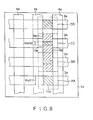
- FIG. 8 is a plane view showing the semiconductor substrate on which the memory cell array is formed;
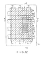
- Figs. 9 and 12 are plane views for assistance in explaining the manufacturing process of the memory cell array shown in Fig. 8;
- Fig. 10 is a cross-sectional view taken along the line F -F' shown in Fig. 9;
- Fig. 11 is a cross-sectional view taken along the line E - E' shown in Fig. 9;
- Fig. 13 is a cross-sectional view taken along the line F - F' shown in Fig. 12;
- Fig. 14 is a cross-sectional view taken along the line E - E' shown in Fig. 12;
- Fig. 15 is the current and voltage characteristics of the memory cell shown in Fig. 8.
- a plurality of straight n + type impurity diffusion regions 4a are formed on the principal plane of a p-type semiconductor substrate 1 a. Further, on the principal plane thereof, a gate insulating film 2a of silicon oxide (shown in Fig. 10) is formed .
- a plurality of gate electrodes 3a of poly silicon are formed on the semiconductor substrate 1 via the gate insulating film 2a so as to cross the n + impurity diffusion regions 4a, respectively.
- a pair of adjacent impurity diffusion regions 4a formed under the two adjacent gate electrodes 3a are source and drain regions, and a region formed between the source and drain regions 4a is used as the channel region so as to form one memory cell.
- a plurality of memory cells AA, BB. CC, DD, .. are arranged into a matrix pattern.
- two bit information data can be recorded in one memory cell by changing the channel conductance gm (by changing the channel width Weff) and further by changing the threshold voltage (by changing the ion implantation rate).
- the channel conductance and the threshold voltage of the memory cell are controlled.
- the threshold voltage these memory cells CC and DD is set to Vth2, which is higher than that Vth1 of the memory cells AA and BB into which no ions are implanted.
- a plurality of memory cells have either one of the two channel widths Weff1 and Weff2.
- the p-type impurity diffusion regions 9a are formed on the semiconductor substrate 1 a so as to extend toward and into the channel region 10a.
- the impurity diffusion regions 9a extend into the channel region 10a, it is possible to change the substantial width of the channel region 10a.
- Fig. 8 In the case shown in Fig.
- the substantial channel width of the memory cells BB and CC is reduced to Weff2 by forming the p-type impurity diffusion regions 9a on both sides thereof, as compared with the channel width Weff1 of the channel region 10b of the memory cells AA and DD having no regions 9a, respectively. Further, it is unnecessary to form the two impurity diffusion regions 9a on both sides of the channel region 10a so as to sandwich the channel region 10a; that is, it is possible to change the channel width of the channel region 10a by forming only the single impurity diffusion region 9a (e.g., on the side of the memory cell DD in Fig. 8).
- the respective memory cells have a high threshold voltage (as in the memory cells CC and DD) and a low threshold voltage (as in the memory cells AA and BB) and further a substantially wide channel width (as in the memory cells AA and DD) and a substantially narrow channel width (as in the memory cells BB and CC), respectively, when these threshold voltages and channel widths are combined with each other, it is possible to realize 4 states of the memory cells, so that the four memory cells AA, BB, CC and DD have 4 different memory states, as shown in Fig. 15.
- the silicon oxide film 2a (shown in Fig. 10) with a thickness of about 20 nm is formed on the p-type silicon semiconductor substrate 1a, and further the poly silicon gate electrodes 3a with a thickness of about 40 nm are formed on the silicon oxide film 2a in accordance with CVD (chemical vapor deposition).
- These gate electrodes 3a are doped to n-type by diffusing phosphorus.
- the n-type impurity diffusion regions 4a for instance are formed by implanting arsenic ions at an ion implantation rate of 3 x 10 15 cm- 2 .
- ions are implanted at a low acceleration voltage of 40 keV and at an ion implantation rate of 5 x 10 12 to 1 x 10 13 cm- 2 for prevention of reversal of the conductivity types.
- the process of impurity ion implantation for changing the threshold voltage of the predetermined memory cells of the memory sell array formed on the semiconductor substrate 1 a will be explained.
- the n type impurity diffusion regions 4a are formed as the source and drain regions roughly at regular intervals in stripe shape.
- the silicon oxide film 2a is formed on the principal plane of the semiconductor substrate 1a, and the poly silicon gate electrodes 3a are formed on the silicon oxide film 2a roughly at regular intervals in stripe shape.
- the gate electrodes 3a are formed so as to cross the n-type impurity diffusion regions 4a at roughly right angles.
- a photoresist 5 is applied to all over the surface of the principal plane of the semiconductor substrate 1a, and openings 51 for exposing the predetermined memory cells (CC and DD) are formed by patterning the photoresist 5 by use of a first data forming mask. Then, boron ions 6 are implanted at 160 keV and at 1 x 10 13 to 1 x 10 14 cm- 2 , with the result that ions 6 can be implanted into the channel regions of the memory cells CC and DD.
- boron ions 6 implanted into the gate electrode 3a reach the surface region of the semiconductor substrate 1 under the gate electrode 3a, since baron ions 6 implanted directly to the surface of the semiconductor substrate 1 a reach deep (about 0.5 ⁇ m or deeper) into semiconductor substrate 1a, these ions will not exert influence upon the threshold voltage and the channel width by the subsequent heat treatment effected after the manufacturing process.
- the photoresist 5 is removed. Further, another photoresist 7 is formed all over the principal surface of the semiconductor substrate 1 a, as shown in Fig. 12, and openings 71 for exposing the predetermined memory cells (BB and CC) are formed by patterning the photoresist 7 by use of a second data forming mask. Further, as shown in Figs. 13 and 14, boron ions 8 are implanted into the semiconductor substrate 1 a via the photoresist 7 and through the openings 71 at a low acceleration voltage (40 keV). Since being implanted at the low acceleration voltage, boron ions 8 cannot pass through the gate electrodes 3a but implanted only the surface region of the semiconductor substrate 1 a on both sides of the gate electrodes 3a.
- a low acceleration voltage 40 keV
- the semiconductor substrate 1 a is heat treated at about 900 to 950 °C for about one hour.
- boron ions are diffused in the lateral direction of the silicon semiconductor substrate 1a, so that p + impurity diffusion regions 9a can be formed so as to extend toward and into the channel regions formed under the gate electrodes 3a of the memory cells BB and CC, respectively.
- p + impurity diffusion regions 9a can be formed so as to extend toward and into the channel regions formed under the gate electrodes 3a of the memory cells BB and CC, respectively.
- the p + impurity diffusion regions 9a are not formed, so that the effective channel width Weff1 is kept at 0.5 ⁇ m, for instance.
- the p + impurity diffusion regions 9a extend to the channel regions formed under the gate electrodes 3a, so that the effective channel width Weff2 of the memory cells can be reduced to such an extent as 0.25 ⁇ m.
- the memory cell AA having the low threshold voltage Vth1 and the wide channel width Weff1 is provided with the first current and voltage characteristics (1); the memory cell BB having the low threshold voltage Vth1 and the narrow channel width Weff2 is provided with the second current and voltage characteristics (2); the memory call DD having the high threshold voltage Vth2 and the wide channel width Weff1 is provided with the third current and voltage characteristics (3); and the memory cell DD having the high threshold voltage Vth2 and the narrow channel width Weff2 is provided with the fourth current and voltage characteristics (4).
- the present invention can be applied to NAND type transistors.
- 4 states can be obtained by changing only the channel width and further 2 states can be obtained by changing only the threshold voltage. Accordingly, when these two methods are combined with each other, it is possible to obtain 8-state ROM, so that 3-bit information can be stored in one memory cell array. In contrast with this, to store 3-bit data in one memory cell array, it is also possible to obtain an 8-state ROM on the basis of 2 states obtained by changing the channel width and 4 states obtained by changing the threshold voltage.
- the p-type silicon semiconductor substrate is used, without being limited thereto, it is of course possible to use an n-type silicon semiconductor substrate.
- the channel conductance can be changed easily by controlling the channel width accurately on the basis of the impurity diffusion regions formed in the semiconductor substrate.
- the semiconductor device provided with a multi-stat ROM can be realized, in which a plurality of read states can be obtained by changing the channel conductance accurately on the basis of change in the channel width (even if there exists an alignment error of the photoresist) and the threshold voltage in combination.
Landscapes
- Engineering & Computer Science (AREA)
- Microelectronics & Electronic Packaging (AREA)
- Computer Hardware Design (AREA)
- Semiconductor Memories (AREA)
- Dram (AREA)
- Read Only Memory (AREA)
- Semiconductor Integrated Circuits (AREA)
- Insulated Gate Type Field-Effect Transistor (AREA)
Applications Claiming Priority (2)
| Application Number | Priority Date | Filing Date | Title |
|---|---|---|---|
| JP3768794A JPH07226446A (ja) | 1994-02-12 | 1994-02-12 | 半導体装置及びその製造方法 |
| JP37687/94 | 1994-02-12 |
Publications (2)
| Publication Number | Publication Date |
|---|---|
| EP0667644A1 true EP0667644A1 (fr) | 1995-08-16 |
| EP0667644B1 EP0667644B1 (fr) | 1997-08-27 |
Family
ID=12504495
Family Applications (1)
| Application Number | Title | Priority Date | Filing Date |
|---|---|---|---|
| EP95101831A Expired - Lifetime EP0667644B1 (fr) | 1994-02-12 | 1995-02-10 | Procédé de fabrication d'un dispositif semi-conducteur pour enregistrer plusieurs états |
Country Status (6)
| Country | Link |
|---|---|
| US (2) | US5629548A (fr) |
| EP (1) | EP0667644B1 (fr) |
| JP (1) | JPH07226446A (fr) |
| KR (1) | KR950025987A (fr) |
| DE (1) | DE69500586T2 (fr) |
| TW (1) | TW275149B (fr) |
Families Citing this family (15)
| Publication number | Priority date | Publication date | Assignee | Title |
|---|---|---|---|---|
| US5693551A (en) * | 1995-09-19 | 1997-12-02 | United Microelectronics, Corporation | Method for fabricating a tri-state read-only memory device |
| JP3634086B2 (ja) | 1996-08-13 | 2005-03-30 | 株式会社半導体エネルギー研究所 | 絶縁ゲイト型半導体装置の作製方法 |
| JP4014676B2 (ja) | 1996-08-13 | 2007-11-28 | 株式会社半導体エネルギー研究所 | 絶縁ゲイト型半導体装置およびその作製方法 |
| JP4103968B2 (ja) | 1996-09-18 | 2008-06-18 | 株式会社半導体エネルギー研究所 | 絶縁ゲイト型半導体装置 |
| KR100500033B1 (ko) | 1996-10-15 | 2005-09-08 | 가부시키가이샤 한도오따이 에네루기 켄큐쇼 | 반도체장치 |
| JP4104701B2 (ja) * | 1997-06-26 | 2008-06-18 | 株式会社半導体エネルギー研究所 | 半導体装置 |
| US6686623B2 (en) * | 1997-11-18 | 2004-02-03 | Semiconductor Energy Laboratory Co., Ltd. | Nonvolatile memory and electronic apparatus |
| JP4236722B2 (ja) * | 1998-02-05 | 2009-03-11 | 株式会社半導体エネルギー研究所 | 半導体装置の作製方法 |
| US6238982B1 (en) * | 1999-04-13 | 2001-05-29 | Advanced Micro Devices | Multiple threshold voltage semiconductor device fabrication technology |
| US6724037B2 (en) * | 2000-07-21 | 2004-04-20 | Semiconductor Energy Laboratory Co., Ltd. | Nonvolatile memory and semiconductor device |
| US6683337B2 (en) * | 2001-02-09 | 2004-01-27 | Micron Technology, Inc. | Dynamic memory based on single electron storage |
| KR100650867B1 (ko) * | 2005-12-29 | 2006-11-28 | 동부일렉트로닉스 주식회사 | 협채널 금속 산화물 반도체 트랜지스터 |
| US20120244668A1 (en) * | 2011-03-25 | 2012-09-27 | Jeesung Jung | Semiconductor devices with layout controlled channel and associated processes of manufacturing |
| US8742481B2 (en) | 2011-08-16 | 2014-06-03 | Micron Technology, Inc. | Apparatuses and methods comprising a channel region having different minority carrier lifetimes |
| US10069015B2 (en) | 2016-09-26 | 2018-09-04 | International Business Machines Corporation | Width adjustment of stacked nanowires |
Citations (4)
| Publication number | Priority date | Publication date | Assignee | Title |
|---|---|---|---|---|
| US4272830A (en) * | 1978-12-22 | 1981-06-09 | Motorola, Inc. | ROM Storage location having more than two states |
| US4395725A (en) * | 1980-10-14 | 1983-07-26 | Parekh Rajesh H | Segmented channel field effect transistors |
| EP0119729A1 (fr) * | 1983-02-14 | 1984-09-26 | Fujitsu Limited | Dispositif de mémoire à semi-conducteur |
| EP0448141A1 (fr) * | 1990-02-27 | 1991-09-25 | STMicroelectronics S.r.l. | Procédé de programmation apte à définir au moins quatre niveaux différents de courant dans une cellule de mémoire ROM |
Family Cites Families (7)
| Publication number | Priority date | Publication date | Assignee | Title |
|---|---|---|---|---|
| US4317273A (en) * | 1979-11-13 | 1982-03-02 | Texas Instruments Incorporated | Method of making high coupling ratio DMOS electrically programmable ROM |
| US4811066A (en) * | 1987-10-19 | 1989-03-07 | Motorola, Inc. | Compact multi-state ROM cell |
| US5168465A (en) * | 1988-06-08 | 1992-12-01 | Eliyahou Harari | Highly compact EPROM and flash EEPROM devices |
| JPH03185758A (ja) * | 1989-12-14 | 1991-08-13 | Sharp Corp | 半導体装置の製造方法 |
| US5285069A (en) * | 1990-11-21 | 1994-02-08 | Ricoh Company, Ltd. | Array of field effect transistors of different threshold voltages in same semiconductor integrated circuit |
| JPH0555566A (ja) * | 1991-08-28 | 1993-03-05 | Nec Corp | 半導体装置 |
| US5306657A (en) * | 1993-03-22 | 1994-04-26 | United Microelectronics Corporation | Process for forming an FET read only memory device |
-
1994
- 1994-02-12 JP JP3768794A patent/JPH07226446A/ja active Pending
-
1995
- 1995-02-10 KR KR1019940002480A patent/KR950025987A/ko active Granted
- 1995-02-10 EP EP95101831A patent/EP0667644B1/fr not_active Expired - Lifetime
- 1995-02-10 DE DE69500586T patent/DE69500586T2/de not_active Expired - Lifetime
- 1995-02-10 US US08/386,477 patent/US5629548A/en not_active Expired - Fee Related
- 1995-02-15 TW TW084101364A patent/TW275149B/zh not_active IP Right Cessation
-
1996
- 1996-12-20 US US08/771,287 patent/US5885872A/en not_active Expired - Fee Related
Patent Citations (4)
| Publication number | Priority date | Publication date | Assignee | Title |
|---|---|---|---|---|
| US4272830A (en) * | 1978-12-22 | 1981-06-09 | Motorola, Inc. | ROM Storage location having more than two states |
| US4395725A (en) * | 1980-10-14 | 1983-07-26 | Parekh Rajesh H | Segmented channel field effect transistors |
| EP0119729A1 (fr) * | 1983-02-14 | 1984-09-26 | Fujitsu Limited | Dispositif de mémoire à semi-conducteur |
| EP0448141A1 (fr) * | 1990-02-27 | 1991-09-25 | STMicroelectronics S.r.l. | Procédé de programmation apte à définir au moins quatre niveaux différents de courant dans une cellule de mémoire ROM |
Non-Patent Citations (2)
| Title |
|---|
| D.A. RICH ET AL., IEEE JOURNAL OF SOLID-STATE CIRCUITS, vol. SC-19, no. 2, April 1984 (1984-04-01), NEW YORK, USA, pages 174 - 179 * |
| K. BERNSTEIN, IBM TECHNICAL DISCLOSURE BULLETIN, vol. 23, no. 10, March 1981 (1981-03-01), pages 4461 * |
Also Published As
| Publication number | Publication date |
|---|---|
| TW275149B (fr) | 1996-05-01 |
| US5629548A (en) | 1997-05-13 |
| KR950025987A (ko) | 1995-09-18 |
| JPH07226446A (ja) | 1995-08-22 |
| DE69500586T2 (de) | 1998-02-05 |
| EP0667644B1 (fr) | 1997-08-27 |
| US5885872A (en) | 1999-03-23 |
| DE69500586D1 (de) | 1997-10-02 |
Similar Documents
| Publication | Publication Date | Title |
|---|---|---|
| JP2689888B2 (ja) | 半導体装置及びその製造方法 | |
| US5641699A (en) | Method of manufacturing a semiconductor device having a dummy cell | |
| US5629548A (en) | Semiconductor device with adjustable channel width | |
| KR960009994B1 (ko) | 반도체 메모리 장치 및 그 제조방법 | |
| US5300804A (en) | Mask ROM device having highly integrated memory cell structure | |
| US6359303B1 (en) | Split gate flash memory with virtual ground array structure and method of fabricating the same | |
| JPH05102436A (ja) | 半導体メモリ装置とその製造方法 | |
| US5777920A (en) | Semiconductor memory device and method of manufacturing the same | |
| US5616948A (en) | Semiconductor device having electrically coupled transistors with a differential current gain | |
| US5545580A (en) | Multi-state read-only memory using multiple polysilicon selective depositions | |
| US6051469A (en) | Method of fabricating bit line | |
| EP0021776B1 (fr) | Dispositif semi-conducteur de mémoire et procédé pour sa fabrication | |
| US5828113A (en) | Double density MROM array structure | |
| JP3426424B2 (ja) | 半導体記憶装置及びその製造方法 | |
| US5311463A (en) | Semiconductor memory device and manufacturing method thereof | |
| US5883405A (en) | MOS transistor read-only memory device | |
| US4263663A (en) | VMOS ROM Array | |
| US5949704A (en) | Stacked read-only memory | |
| JPH03153085A (ja) | 半導体記憶装置及びその製造方法 | |
| KR100190034B1 (ko) | 스태틱 랜덤 억세스 메모리장치 | |
| KR0147649B1 (ko) | 불휘발성 반도체 메모리 장치 제조방법 | |
| JPH09275152A (ja) | 半導体記憶装置の製造方法 | |
| EP0925609B1 (fr) | Piles de memoires rom | |
| CN87106738A (zh) | 半导体器件及其制造方法 | |
| JP3411346B2 (ja) | 半導体メモリ装置とその製造方法 |
Legal Events
| Date | Code | Title | Description |
|---|---|---|---|
| PUAI | Public reference made under article 153(3) epc to a published international application that has entered the european phase |
Free format text: ORIGINAL CODE: 0009012 |
|
| 17P | Request for examination filed |
Effective date: 19950210 |
|
| AK | Designated contracting states |
Kind code of ref document: A1 Designated state(s): DE FR GB |
|
| 17Q | First examination report despatched |
Effective date: 19951013 |
|
| GRAG | Despatch of communication of intention to grant |
Free format text: ORIGINAL CODE: EPIDOS AGRA |
|
| GRAH | Despatch of communication of intention to grant a patent |
Free format text: ORIGINAL CODE: EPIDOS IGRA |
|
| GRAH | Despatch of communication of intention to grant a patent |
Free format text: ORIGINAL CODE: EPIDOS IGRA |
|
| GRAA | (expected) grant |
Free format text: ORIGINAL CODE: 0009210 |
|
| AK | Designated contracting states |
Kind code of ref document: B1 Designated state(s): DE FR GB |
|
| REF | Corresponds to: |
Ref document number: 69500586 Country of ref document: DE Date of ref document: 19971002 |
|
| ET | Fr: translation filed | ||
| PLBE | No opposition filed within time limit |
Free format text: ORIGINAL CODE: 0009261 |
|
| STAA | Information on the status of an ep patent application or granted ep patent |
Free format text: STATUS: NO OPPOSITION FILED WITHIN TIME LIMIT |
|
| 26N | No opposition filed | ||
| REG | Reference to a national code |
Ref country code: GB Ref legal event code: IF02 |
|
| PGFP | Annual fee paid to national office [announced via postgrant information from national office to epo] |
Ref country code: FR Payment date: 20100223 Year of fee payment: 16 |
|
| PGFP | Annual fee paid to national office [announced via postgrant information from national office to epo] |
Ref country code: GB Payment date: 20100202 Year of fee payment: 16 Ref country code: DE Payment date: 20100219 Year of fee payment: 16 |
|
| GBPC | Gb: european patent ceased through non-payment of renewal fee |
Effective date: 20110210 |
|
| REG | Reference to a national code |
Ref country code: FR Ref legal event code: ST Effective date: 20111102 |
|
| REG | Reference to a national code |
Ref country code: DE Ref legal event code: R119 Ref document number: 69500586 Country of ref document: DE Effective date: 20110901 |
|
| PG25 | Lapsed in a contracting state [announced via postgrant information from national office to epo] |
Ref country code: FR Free format text: LAPSE BECAUSE OF NON-PAYMENT OF DUE FEES Effective date: 20110228 |
|
| PG25 | Lapsed in a contracting state [announced via postgrant information from national office to epo] |
Ref country code: GB Free format text: LAPSE BECAUSE OF NON-PAYMENT OF DUE FEES Effective date: 20110210 |
|
| PG25 | Lapsed in a contracting state [announced via postgrant information from national office to epo] |
Ref country code: DE Free format text: LAPSE BECAUSE OF NON-PAYMENT OF DUE FEES Effective date: 20110901 |