EP0668511A2 - Gerät oder Methode zum Fühlen eines Magnetfeldes; Fühler zum Informationslesen von einem Magnetospeichermedium magnetoresistives Element; magnetfeldgesteuerter Schalter - Google Patents
Gerät oder Methode zum Fühlen eines Magnetfeldes; Fühler zum Informationslesen von einem Magnetospeichermedium magnetoresistives Element; magnetfeldgesteuerter Schalter Download PDFInfo
- Publication number
- EP0668511A2 EP0668511A2 EP95301043A EP95301043A EP0668511A2 EP 0668511 A2 EP0668511 A2 EP 0668511A2 EP 95301043 A EP95301043 A EP 95301043A EP 95301043 A EP95301043 A EP 95301043A EP 0668511 A2 EP0668511 A2 EP 0668511A2
- Authority
- EP
- European Patent Office
- Prior art keywords
- magnetic field
- current path
- magnetoresistive element
- sensor according
- variable resistance
- Prior art date
- Legal status (The legal status is an assumption and is not a legal conclusion. Google has not performed a legal analysis and makes no representation as to the accuracy of the status listed.)
- Granted
Links
- 230000005291 magnetic effect Effects 0.000 title claims abstract description 100
- 238000000034 method Methods 0.000 title claims 2
- 230000007423 decrease Effects 0.000 claims description 14
- 230000005294 ferromagnetic effect Effects 0.000 claims description 11
- 239000003302 ferromagnetic material Substances 0.000 claims description 3
- 239000000696 magnetic material Substances 0.000 claims description 2
- 239000000463 material Substances 0.000 claims 16
- 238000001514 detection method Methods 0.000 claims 1
- 230000007704 transition Effects 0.000 description 21
- 239000010408 film Substances 0.000 description 4
- 230000005381 magnetic domain Effects 0.000 description 3
- 230000005330 Barkhausen effect Effects 0.000 description 2
- 230000005415 magnetization Effects 0.000 description 2
- 229910001092 metal group alloy Inorganic materials 0.000 description 2
- 229910000889 permalloy Inorganic materials 0.000 description 2
- 239000002131 composite material Substances 0.000 description 1
- 230000000694 effects Effects 0.000 description 1
- 238000004880 explosion Methods 0.000 description 1
- 231100001261 hazardous Toxicity 0.000 description 1
- 230000002427 irreversible effect Effects 0.000 description 1
- 239000000203 mixture Substances 0.000 description 1
- 230000035699 permeability Effects 0.000 description 1
- 230000006641 stabilisation Effects 0.000 description 1
- 238000011105 stabilization Methods 0.000 description 1
- 239000000758 substrate Substances 0.000 description 1
- 239000010409 thin film Substances 0.000 description 1
- 230000036962 time dependent Effects 0.000 description 1
Images


Classifications
-
- G—PHYSICS
- G11—INFORMATION STORAGE
- G11B—INFORMATION STORAGE BASED ON RELATIVE MOVEMENT BETWEEN RECORD CARRIER AND TRANSDUCER
- G11B5/00—Recording by magnetisation or demagnetisation of a record carrier; Reproducing by magnetic means; Record carriers therefor
- G11B5/48—Disposition or mounting of heads or head supports relative to record carriers ; arrangements of heads, e.g. for scanning the record carrier to increase the relative speed
- G11B5/488—Disposition of heads
-
- G—PHYSICS
- G11—INFORMATION STORAGE
- G11B—INFORMATION STORAGE BASED ON RELATIVE MOVEMENT BETWEEN RECORD CARRIER AND TRANSDUCER
- G11B5/00—Recording by magnetisation or demagnetisation of a record carrier; Reproducing by magnetic means; Record carriers therefor
- G11B5/02—Recording, reproducing, or erasing methods; Read, write or erase circuits therefor
- G11B5/09—Digital recording
-
- G—PHYSICS
- G11—INFORMATION STORAGE
- G11B—INFORMATION STORAGE BASED ON RELATIVE MOVEMENT BETWEEN RECORD CARRIER AND TRANSDUCER
- G11B5/00—Recording by magnetisation or demagnetisation of a record carrier; Reproducing by magnetic means; Record carriers therefor
- G11B5/127—Structure or manufacture of heads, e.g. inductive
- G11B5/33—Structure or manufacture of flux-sensitive heads, i.e. for reproduction only; Combination of such heads with means for recording or erasing only
- G11B5/39—Structure or manufacture of flux-sensitive heads, i.e. for reproduction only; Combination of such heads with means for recording or erasing only using magneto-resistive devices or effects
-
- H—ELECTRICITY
- H03—ELECTRONIC CIRCUITRY
- H03K—PULSE TECHNIQUE
- H03K17/00—Electronic switching or gating, i.e. not by contact-making and –breaking
- H03K17/94—Electronic switching or gating, i.e. not by contact-making and –breaking characterised by the way in which the control signals are generated
- H03K17/965—Switches controlled by moving an element forming part of the switch
- H03K17/97—Switches controlled by moving an element forming part of the switch using a magnetic movable element
Definitions
- the present invention relates to apparatus for sensing a magnetic field, a sensor for reading information from a magnetic storage medium, and a switch, all employing a magnetoresistive element.
- the present invention also relates to a novel type of magnetoresistive element.
- Magnetoresistive (MR) sensors are used in magnetic storage systems to detect magnetically encoded information from a magnetic storage medium or disc.
- a time dependent magnetic field from a magnetic storage medium or disc directly modulates the resistivity of the MR sensor.
- the change in resistance of the MR sensor can be detected by passing a sense current through the MR sensor and measuring the voltage across the MR sensor. The resulting signal can be used to recover the encoded information from the magnetic storage medium or disc.
- Magnetic MR sensors are typically formed using ferromagnetic metal alloys because of their high magnetic permeability.
- a ferromagnetic metal alloy is deposited in a thin film upon an electrically insulated substrate or wafer. Changing magnetic fields originating from the magnetic storage medium produce a change in the magnetization direction of the MR sensor and thereby change the resistance of the sensor. This phenomenon is called an MR effect.
- MR sensors have a maximum signal-to-noise ratio when the active region of the sensor has no movable magnetic domain boundaries or no domain boundaries.
- the active sense area of the MR sensor should be a single domain.
- Barkhausen noise a phenomenon caused by the irreversible motion of a magnetic domain in the presence of an applied magnetic field. Barkhausen noise cannot occur if no domain boundaries exist.
- a single magnetic domain MR sensor is achieved by either utilizing geometry, or via boundary control stabilization or inherent longitudinal magnetic fields or any combination thereof.
- apparatus for sensing a magnetic field comprising a magnetoresistive element characterised by having two current paths therein, each of the current paths being such its resistance varies in dependence upon the position of the magnetic field relative thereto.
- a sensor for reading information from a magnetic storage medium comprising the apparatus of the preceding paragraph arranged for sensing the magnetic field representing the information stored on the medium.
- a switch characterised by comprising a magnetoresistive element having two current paths therein, each of the current paths being such that its resistance varies in dependence upon the position of a magnetic field relative thereto, and detecting means for detecting the difference between the respective resistances of the current paths and producing a switch output indicative thereof, such that the switch output is controlled by the position of the magnetic field relative to the respective current paths.
- a magnetoresistive element characterised by comprising layers of magnetic and layers of non-magnetic material.
- the magnetoresistive element comprises layers of ferromagnetic and layers of non-ferromagnetic material.
- GMRs giant magnetoresistive elements
- the above apparatus, sensor and switch advantageously include such a magnetoresistive element.
- the magnetoresistive elements may have multi-layered structures. These devices may include either layers of ferromagnetic and non-ferromagnetic films or a similar set of films. Permalloy may or may not be part of the layered pattern.
- GMR sensors the change in resistivity, due to a given magnetic field, as defined by ⁇ ⁇ ⁇ can be in excess of 65 percent compared to between 0.5% and 2.0% for standard devices.
- Giant MR sensors belong to a class of sensors in which the current density vector J ⁇ functionally depends on the spatial variation of ⁇ ( ⁇ ) via spatial field gradients. Hence the dependence of the current density vector J ⁇ on the resistivity of the device ⁇ is critical.
- magnetoresistive elements may allow the reading of information from a magnetic storage medium due to a change in resistance of various positions along a length of the giant magnetoresistive element caused by an applied magnetic field.
- One embodiment of the present invention is a magnetoresistive sensor for reading information from a longitudinal track of a magnetic storage medium moving under the sensor.
- the sensor includes a giant magnetoresistive element positioned on a bottom surface of a side rail located adjacent to the track. With the giant magnetoresistive element, the current density vector J ⁇ can be dynamically adjusted by applying a magnetic field to the element.
- First, second, and third electrical contacts are spatially and preferably symmetrically positioned on the giant magnetoresistive element and along the track.
- a first current path having a first variable resistance is formed between the first and second electrical contacts, while a second current path having a second variable resistance is formed between the first and third electrical contacts.
- the first and second current paths are preferably symmetrically positioned about the first electrical contact.
- a magnetic field representing information from the track of the magnetic storage medium passes under the giant magnetoresistive element causing a change in the first variable resistance in the first current path when the magnetic field passes under the first current path.
- the magnetic field causes a change in the second variable resistance in the second current path when the magnetic field passes under the second current path.
- External electrical circuitry can manipulate the various signal changes resulting from these resistance variations, thereby recovering the desired information from the magnetic storage medium.
- the property of a giant magnetoresistive sensor allowing for a large change in resistance in the presence of a magnetic field is utilized to unbalance a current flow detectable by external circuitry.
- a second embodiment of the present invention is an apparatus for sensing a change in a magnetic field.
- the apparatus includes a giant magnetoresistive element positioned adjacent to the magnetic field.
- First. second, and third electrical contacts are spatially positioned on the giant magnetoresistive element forming a first current path having a first variable resistance between the first and second electrical contacts and a second current path having a second variable resistance between the first and third electrical contacts.
- the first and second current paths are symmetrically positioned about the first contact.
- the magnetic field causes a change in the first resistance in the first current path when the magnetic field passes underneath the first current path, and the magnetic field causes a change in the second resistance in the second current path when the magnetic field passes underneath the second current path.
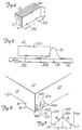
- Figure 1 is a diagrammatic view of a slider containing a giant magnetoresistive element.
- Figure 2 is a greatly enlarged diagrammatic view of the trailing edge of a slider incorporating a first embodiment of the present invention.
- Figure 3 is a greatly enlarged diagrammatic view of the trailing edge of a slider incorporating a second embodiment of the present invention.
- Figure 4 is a diagrammatic view of a giant magnetoresistive element.
- Figure 5 is a side view of a giant magnetoresistive element and a track of a magnetic storage medium moving thereunder.
- Figure 6 is a greatly enlarged diagrammatic view of the trailing edge of a slider incorporating an embodiment of the present invention.
- Figure 7 is a diagrammatic representation of the contacts of a giant magnetoresistive element and the resistance paths between the contacts.
- Figure 8A is a diagrammatic view showing an embodiment of the present invention incorporated into a first electrical circuit.
- Figure 8B is a graph showing the output voltage of the electrical circuit of Figure 8A as a function of the position of a transition from a magnetic storage medium.
- Figure 9A is a diagrammatic view showing an embodiment of the present invention incorporated into a second electrical circuit.
- Figure 9B is a graph showing the output voltage of the electrical circuit of Figure 9A as a function of the position of a magnetic medium.
- FIG. 1 is a diagrammatic view of slider 10.
- Slider 10 includes leading edge 12, trailing edge 14, first side rail 16, second side rail 18, and giant magnetoresistive (GMR) element 20.
- First side rail 16 includes outer surface 22 and bottom surface 24, while second side rail 18 includes outer surface 26 and bottom surface 28.
- GMR giant magnetoresistive
- slider 10 having GMR element 20 positioned on first side rail 16 is attached to an arm of a disc drive system and used for recording information to and reading information from a magnetic storage medium or disc.
- a second GMR element similar to GMR element 20, is positioned on second side rail 18.
- FIG. 2 is a greatly enlarged diagrammatic view of trailing edge 14 of slider 10 incorporating a first embodiment of the present invention.
- Slider 10 shown in Figure 2 includes trailing edge 14, first side rail 16 having outer surface 22 and bottom surface 24, second side rail 18 having outer surface 26 and bottom surface 28, and GMR element 20.
- GMR element 20 includes electrical contacts 30A, 30B and 30C and has length L and height H. Due to the resistive nature of GMR element 20, a first current path is formed between electrical contacts 30A and 30B and a second current path is formed between contacts 30A and 30C. Electrical leads (not shown in Figure 2) are used to connect electrical contacts 30A, 30B and 30C to external circuitry.
- slider 20 is positioned above a moving magnetic storage medium or disc.
- the magnetic storage medium or disc contains a series of data tracks, one of which is represented by track 32.
- Track 32 contains a series of longitudinal transitions 34. Each transition on track 32 represents a particular piece of data stored on track 32 and has a magnetic field associated with it.
- Magnetic field 36 (shown in Figure 2) is associated with longitudinal transition 34 and denotes the vertical field profile as a function of the distance from transition 34.
- Track 32 moves in the direction from leading edge 12 to trailing edge 14 of slider 10, as shown by the arrow 35 in Figure 2.
- FIG 3 is a greatly enlarged diagrammatic view of trailing edge 14 of slider 10 incorporating a second embodiment of the present invention.
- the embodiment shown in Figure 3 is another example of a composite structure permitting a conventional writer structure (not shown in Figure 3) to be added.
- Slider 10, as shown in Figure 3 is identical to the slider shown in Figure 2, except that GMR element 20 is no longer positioned on outer surface 22 of first side rail 16. Rather, first GMR element 20 is located within core 38 positioned on trailing edge 14 of first side rail 16, and second GMR element 40 is located within core 42 positioned on trailing edge 14 of second side rail 18.
- GMR element 40 includes contacts (not shown) similar to contacts 30A, 30B and 30C of GMR element 20. GMR elements 20 and 40 are identical; therefore, for simplicity, only GMR element 20 will be further discussed.
- GMR element 20 is positioned such that the length of GMR element 20 is substantially parallel to track 32 moving under first side rail 16. This positioning, and the position of contacts 30A, 30B and 30C permit a large change in resistance within the first and second current paths as magnetic field 36 passes thereunder, thereby unbalancing a current flow detectable by external circuitry.
- FIG. 4 is a diagrammatic view of GMR element 20.
- GMR element 20 differs from a normal MR element in that GMR element 20 includes either layers of ferromagnetic and non-ferromagnetic films or a similar pattern of films. Standard permalloy may be part of the pattern.
- the novel composition of GMR element 20 provides that the change in resistivity of GMR element 20 can be significantly modulated by the movement of a magnetic field. By properly positioning electrical contacts 30A, 30B and 30C, it is possible to change the resistance in the first and second current paths formed by contacts 30A, 30B and 30C. This change in resistance can then be manipulated by external circuitry to decode transition 34 located on track 32 associated with magnetic field 36.
- Contacts 30A, 30B and 30C can be positioned anywhere along thickness T of GMR element 20.
- contacts 30A, 30B and 30C are positioned on an outer surface of GMR element 20 as shown in Figure 4.
- contacts 30A, 30B and 30C must be spatially positioned along length L of GMR element 20 in order to transduce the modulated resistivity of GMR element 20.
- contacts 30B and 30C are symmetrically positioned along length L of MR element 20 about contact 30A, thereby forming an isosceles triangle. With this type of design, differing resistances due to differing lengths of current paths are eliminated. Therefore, any resistance changes and associated current splitting should be a result of a moving transition 34 located under the MR element.
- contacts 30A, 30B and 30C are spatially positioned along length L of GMR element 20 and that contact 30A is positioned at a height different from the height from both contacts 30B and 30C.
- the first and second current paths are symmetrically positioned about first contact 30A.
- Figure 5 is a side view of GMR element 20 and track 32 of a magnetic storage medium moving thereunder.
- Track 32 is moving in a direct as shown by the arrow in Figure 5.
- transition 34 and associated magnetic field 36 move under GMR element 20.
- transition 34 and associated magnetic field 36 When transition 34 and associated magnetic field 36 becomes positioned between first contact 30A and second contact 30B, magnetic field 36 causes a decrease in resistance in a first current path between contacts 30A and 30B. This decrease in resistance can be detected by external circuitry by passing a current through a first contact path formed between contacts 30A and 30B. Likewise, when transition 34 and associated field 36 moves to a position between first contact 30A and third contact 30C, the resistance in the second current path formed by contacts 30A and 30C decreases and the resistance in the first current path formed by contacts 30A and 30B increases due to the absence of the magnetic field between contacts 30A and 30B. This change in resistance can be detected by external circuitry by passing a current through second contact path formed by contacts 30A and 30C, thereby decoding transition 34.
- Figure 6 is a greatly enlarged diagrammatic view of trailing edge 14 of slider 10 incorporating a first embodiment of the present invention.
- Figure 6 shows electrical leads 44A, 44B and 44C connected to contacts 30A, 30B and 30C, respectively. Electrical leads 44A, 44B, and 44C provide the current path from external circuitry (not shown in Figure 6) to contacts 30A, 30B and 30C. Although contacts 30A, 30B and 30C are shown on the outside surface of GMR element 20, these contacts can be positioned throughout the width of GMR element 20.
- Figure 7 is a diagrammatic representation of contacts 30A, 30B and 30C and the resistance paths between the contacts.
- resistance R1 When any magnetic field becomes positioned between contacts 30A and 30B, resistance R1 will decrease. This decrease in resistance of R1 is caused by the properties of the GMR element having a plurality of ferromagnetic and non-ferromagnetic layers and can be detected and manipulated by external circuitry connected to electrical leads 44A and 44B.
- resistance R2 decreases. This decrease in resistance can be detected and manipulated by external circuitry connected to contacts 44A and 44C. External circuitry can utilize these changes in resistances of R1 and R2 for a variety of purposes, as discussed below.
- Figure 8A is a diagrammatic view showing the GMR element 20 incorporated into a first electrical circuit.
- Figure 8A includes GMR element 20, contacts 30A, 30B and 30C, electrical leads 44A, 44B and 44C, resistors R3 and R4, having identical resistances, and differential amplifier 46.
- GMR element 20 is normally positioned on slider 10, either on outer surface 22 of first side rail 16, as shown in Figure 2, or in core 38 of Figure 3.
- Figure 8B is a graph showing the output voltage of differential amplifier 46 as a function of the position of transition 34 and associated magnetic field 36.
- track 32 of a magnetic storage medium or disc is moving underneath slider 10 having GMR element 20 positioned near trailing edge 14.
- transition 34 and associated magnetic field 36 move, they eventually become positioned between contacts 30A and 30B.
- the resistance in the first current path between contacts 30A and 30B decreases due to the properties of GMR element 20.
- the decrease in resistance causes an increase in the current flowing through the first current path from contact 30A to contact 30B, as compared to the current flow through the second current path from contact 30A to contact 30C.
- This increase in current through the first current path provides a greater voltage drop across resistor R3 than the voltage drop across resistor R4.
- the difference in voltage drop across resistors R3 and R4 is amplified by differential amplifier 46, producing a positive output voltage V o . This output voltage is shown on the left side of Figure 8B.
- transition 34 and associated magnetic field 36 becomes positioned directly under contact 30A.
- the change in resistance in the first current path between contacts 30A and 30B will be equal to the change in resistance in the second current path between contacts 30A and 30C. Therefore, there will be no differential voltage drop across resistors R3 and R4. Hence, there will be no output voltage V o of differential amplifier 46.
- transition 34 and associated magnetic field 36 will eventually be positioned substantially under the second current path between contacts 30A and 30C.
- the resistance in the second current path will decrease and the resistance in the first current path will increase, hence, causing more current flow through the second current path than through the first current path.
- This increase in current through the second current path will in turn cause a increase in the voltage across resistor R4.
- the difference in voltage drop across resistors R3 and R4 is amplified by differential amplifier 46, producing a negative output voltage V o . This output voltage is shown on the right side of Figure 8B by the negative output voltage.
- transition 34 and associated magnetic field 36 will move such that magnetic field 36 is no longer positioned under either the first contact path between contacts 30A and 30B or the second contact path positioned between contacts 30A and 30C.
- the voltage drop across resistor R3 will be substantially equal to the voltage drop resistor R4 and the gain of differential amplifier 46 will be zero or nominal.
- the output will continue to be zero or nominal until new data having a separate magnetic field begins to pass under GMR element 20.
- One advantage of such an arrangement is that it may allow signals representative of the magnetic field 36 occurring due to transitions 34 to be decoded by a standard zero crossing detector.
- the information stored on the recording medium may be readily retrieved, for example, by detecting zero crossings in the output voltage V o of the differential amplifier 46.
- Figure 9A is a diagrammatic view showing an embodiment of the present invention incorporated into a second electrical circuit.
- Figure 9A includes GMR element 20, contact 30A, 30B and 30C, electrical leads 44A, 44B and 44C, resistors R3 and R4 having substantially identical resistances, and comparitor 48.
- comparitor 48 is a Schmitt trigger (ie. a comparitor with hysteresis).
- Figure 9B is a graph showing the output voltage of comparitor 48 of Figure 9A as a function of the position of magnetic switch 50.
- magnetic switch 50 is movable from position “a” to position "a'.”
- the resistance in the first current path between contacts 30A and 30B is low due to the properties of GMR element 20.
- the low resistance in resistivity causes an increase in the current flow through the first current path from contact 30A to contact 30B, as compared to the current flow through the second current path from contact 30A to contact 30C.
- This increase in current through the first current path provides a greater voltage drop across resistor R3 than the voltage drop across resistor R4.
- Comparitor 48 interprets this voltage differential and provides a low voltage output, as shown in Figure 9B.
Landscapes
- Engineering & Computer Science (AREA)
- Manufacturing & Machinery (AREA)
- Hall/Mr Elements (AREA)
- Measuring Magnetic Variables (AREA)
- Magnetic Heads (AREA)
Applications Claiming Priority (2)
| Application Number | Priority Date | Filing Date | Title |
|---|---|---|---|
| US198848 | 1994-02-18 | ||
| US08/198,848 US5825593A (en) | 1994-02-18 | 1994-02-18 | Electric field modulated MR sensor |
Publications (3)
| Publication Number | Publication Date |
|---|---|
| EP0668511A2 true EP0668511A2 (de) | 1995-08-23 |
| EP0668511A3 EP0668511A3 (de) | 1997-04-16 |
| EP0668511B1 EP0668511B1 (de) | 2003-11-12 |
Family
ID=22735113
Family Applications (1)
| Application Number | Title | Priority Date | Filing Date |
|---|---|---|---|
| EP95301043A Expired - Lifetime EP0668511B1 (de) | 1994-02-18 | 1995-02-17 | Gerät und Verfahren zum Detektieren eines Magnetfeldes |
Country Status (5)
| Country | Link |
|---|---|
| US (1) | US5825593A (de) |
| EP (1) | EP0668511B1 (de) |
| JP (1) | JPH07254117A (de) |
| DE (1) | DE69532095D1 (de) |
| SG (1) | SG48749A1 (de) |
Cited By (1)
| Publication number | Priority date | Publication date | Assignee | Title |
|---|---|---|---|---|
| WO2001041174A1 (de) * | 1999-12-03 | 2001-06-07 | Siemens Aktiengesellschaft | Elektromagnetisches schaltgerät mit gesteuertem antrieb sowie zugehörig ein verfahren und eine schaltung |
Families Citing this family (6)
| Publication number | Priority date | Publication date | Assignee | Title |
|---|---|---|---|---|
| US5936801A (en) * | 1997-04-04 | 1999-08-10 | Seagate Technology, Inc. | Head slider with partially recessed magnetoresistive element |
| US6633233B1 (en) * | 1999-11-18 | 2003-10-14 | University Of Florida | Acceleration rate meter |
| US7113104B2 (en) * | 2000-11-17 | 2006-09-26 | University Of South Florida | Giant magnetoresistance based gyroscope |
| US6940277B2 (en) * | 2000-11-17 | 2005-09-06 | University Of South Florida | Giant magnetoresistance based nanopositioner encoder |
| US7317596B2 (en) * | 2005-06-21 | 2008-01-08 | Hitachi Global Storage Technologies Netherlands B.V. | Magnetic recording disk drive having read head with high cross-track resolution and disk with low bit-aspect-ratio |
| US8169743B2 (en) * | 2007-07-20 | 2012-05-01 | Hitachi Global Storage Technologies, Netherlands B.V. | Minimizing slider vibration effects on a magnetic transducer |
Family Cites Families (23)
| Publication number | Priority date | Publication date | Assignee | Title |
|---|---|---|---|---|
| US3835377A (en) * | 1970-03-09 | 1974-09-10 | Kogyo Gijutsuin | Three terminal magnetoresistive magnetic field detector in which voltages of opposite polarity relative to ground are applied to opposite ends |
| US3783430A (en) * | 1971-05-24 | 1974-01-01 | Denki Onkyo Co Ltd | Contactless switching apparatus |
| NL7309590A (nl) * | 1973-07-10 | 1975-01-14 | Philips Nv | Inrichting voor het sturen van de positie van een magneetkop ten opzichte van een te volgen informatiespoor. |
| US3855625A (en) * | 1973-12-19 | 1974-12-17 | Ibm | Magnetic head slider assembly |
| JPS576962Y2 (de) * | 1974-07-26 | 1982-02-09 | ||
| JPS52137371A (en) * | 1976-05-13 | 1977-11-16 | Fujitsu Ltd | Position control system |
| IT1211140B (it) * | 1980-12-09 | 1989-09-29 | Sony Corp | Dispositivo commutatore a sensore magnetico. |
| JPS57131078A (en) * | 1981-02-06 | 1982-08-13 | Matsushita Electric Ind Co Ltd | Magnetic sensor |
| JPS5884478A (ja) * | 1981-11-13 | 1983-05-20 | Nec Corp | Mos型磁気抵抗効果素子 |
| JPS5898826A (ja) * | 1981-12-09 | 1983-06-11 | Matsushita Electric Ind Co Ltd | 薄膜磁気ヘツド |
| JPS58211304A (ja) * | 1982-05-31 | 1983-12-08 | Sony Corp | 磁気抵抗素子による磁気信号検出方法 |
| DE3330077A1 (de) * | 1983-08-19 | 1985-02-28 | Siemens AG, 1000 Berlin und 8000 München | Einrichtung zum herauslesen von informationen, die nach dem prinzip der senkrechten magnetisierung in einem aufzeichnungsmedium eingespeichert sind |
| JPS61131204A (ja) * | 1984-11-30 | 1986-06-18 | Fujitsu Ltd | 磁気記録再生回路 |
| JPS61170918A (ja) * | 1985-01-24 | 1986-08-01 | Nippon Telegr & Teleph Corp <Ntt> | 磁気抵抗効果形磁気ヘツド |
| US4851944A (en) * | 1987-02-17 | 1989-07-25 | Magnetic Peripherals Inc. | Ganged MR head sensor |
| US4816947A (en) * | 1987-11-12 | 1989-03-28 | International Business Machines | Single track vertical and horizontal recording read/write head design |
| US5079663A (en) * | 1990-01-29 | 1992-01-07 | International Business Machines Corporation | Magnetoresistive sensor with track following capability |
| US5998040A (en) * | 1990-12-10 | 1999-12-07 | Hitachi, Ltd. | Multilayer which shows magnetoresistive effect and magnetoresistive element using the same |
| US5260652A (en) * | 1992-03-25 | 1993-11-09 | Seagate Technology, Inc. | Magnetoresistive sensor with electrical contacts having variable resistive regions for enhanced sensor sensitivity |
| JPH05275769A (ja) * | 1992-03-25 | 1993-10-22 | Hitachi Maxell Ltd | 磁界センサ |
| EP0565102A2 (de) * | 1992-04-10 | 1993-10-13 | Hitachi Maxell, Ltd. | Magnetische Schichtungen und Magnetköpfe und magnetische Aufnahme-/Wiedergabegeräte, die solche Schichtungen benutzen |
| DE4326999A1 (de) * | 1993-08-11 | 1995-02-16 | Siemens Ag | Vorrichtung zum magnetfeldgesteuerten Schalten |
| JPH07287821A (ja) * | 1994-04-18 | 1995-10-31 | Matsushita Electric Ind Co Ltd | 磁気抵抗効果素子及び磁気抵抗効果型ヘッド |
-
1994
- 1994-02-18 US US08/198,848 patent/US5825593A/en not_active Expired - Lifetime
-
1995
- 1995-02-17 JP JP7029764A patent/JPH07254117A/ja active Pending
- 1995-02-17 SG SG1996001190A patent/SG48749A1/en unknown
- 1995-02-17 DE DE69532095T patent/DE69532095D1/de not_active Expired - Lifetime
- 1995-02-17 EP EP95301043A patent/EP0668511B1/de not_active Expired - Lifetime
Cited By (1)
| Publication number | Priority date | Publication date | Assignee | Title |
|---|---|---|---|---|
| WO2001041174A1 (de) * | 1999-12-03 | 2001-06-07 | Siemens Aktiengesellschaft | Elektromagnetisches schaltgerät mit gesteuertem antrieb sowie zugehörig ein verfahren und eine schaltung |
Also Published As
| Publication number | Publication date |
|---|---|
| JPH07254117A (ja) | 1995-10-03 |
| US5825593A (en) | 1998-10-20 |
| DE69532095D1 (de) | 2003-12-18 |
| EP0668511A3 (de) | 1997-04-16 |
| SG48749A1 (en) | 1998-05-18 |
| EP0668511B1 (de) | 2003-11-12 |
Similar Documents
| Publication | Publication Date | Title |
|---|---|---|
| US5818685A (en) | CIP GMR sensor coupled to biasing magnet with spacer therebetween | |
| EP0484474B1 (de) | Hochdichte signalverstärkung zeigender magnetoresistiver wiedergabekopf mit kurzgeschlossenem doppelelement | |
| US7477490B2 (en) | Single sensor element that is naturally differentiated | |
| US5883763A (en) | Read/write head having a GMR sensor biased by permanent magnets located between the GMR and the pole shields | |
| JP3266550B2 (ja) | 直交型スピン・バルブ読取りヘッド、組合わせヘッド及び磁気ディスク・ドライブ | |
| US4891725A (en) | Magnetoresistive sensor having antiferromagnetic exchange-biased ends | |
| KR940012687A (ko) | 전류 바이어스된 자기 저항 스핀 밸브 센서 | |
| CN1008668B (zh) | 磁阻读出传感器 | |
| US5600238A (en) | Method and apparatus for detecting the linear or rotary position of an object through the use of a variable magnetic shunt disposed in parallel with a yoke air gap | |
| EP0279535A2 (de) | Kopf mit einem magnetoresistiven Aufnehmer | |
| KR970017217A (ko) | 이중 스핀 밸브 센서를 이용한 이중 저기저항 센서 | |
| US5880912A (en) | Magnetic head with biased GMR element and sense current compensation | |
| GB2134307A (en) | Magnetic head | |
| JPH09259410A (ja) | 磁気抵抗型センサ | |
| WO2000019226A1 (en) | Quad-layer gmr sandwich | |
| JP2008525787A (ja) | 調節可能な特性を有する磁気センサ | |
| US5680281A (en) | Edge-biased magnetoresistive sensor | |
| US4255708A (en) | Magnetoresistive position transducer with invariable peak signal | |
| JPH11304413A (ja) | 磁気検出装置 | |
| EP0668511B1 (de) | Gerät und Verfahren zum Detektieren eines Magnetfeldes | |
| US20100149696A1 (en) | Magnetic sensor including an element for generating signals related to resistance changes | |
| JP2000512763A (ja) | ホイートストンブリッジを備える磁界センサ | |
| US5065094A (en) | Two terminal magnetoresistive sensor having DC blocking capacitor | |
| US6714389B1 (en) | Digital magnetoresistive sensor with bias | |
| US5982177A (en) | Magnetoresistive sensor magnetically biased in a region spaced from a sensing region |
Legal Events
| Date | Code | Title | Description |
|---|---|---|---|
| PUAI | Public reference made under article 153(3) epc to a published international application that has entered the european phase |
Free format text: ORIGINAL CODE: 0009012 |
|
| AK | Designated contracting states |
Kind code of ref document: A2 Designated state(s): DE FR GB IT |
|
| PUAL | Search report despatched |
Free format text: ORIGINAL CODE: 0009013 |
|
| AK | Designated contracting states |
Kind code of ref document: A3 Designated state(s): DE FR GB IT |
|
| 17P | Request for examination filed |
Effective date: 19971006 |
|
| RAP1 | Party data changed (applicant data changed or rights of an application transferred) |
Owner name: SEAGATE TECHNOLOGY LLC |
|
| 17Q | First examination report despatched |
Effective date: 20010618 |
|
| RTI1 | Title (correction) |
Free format text: APPARATUS AND METHOD FOR SENSING A MAGNETIC FIELD |
|
| GRAH | Despatch of communication of intention to grant a patent |
Free format text: ORIGINAL CODE: EPIDOS IGRA |
|
| GRAS | Grant fee paid |
Free format text: ORIGINAL CODE: EPIDOSNIGR3 |
|
| GRAA | (expected) grant |
Free format text: ORIGINAL CODE: 0009210 |
|
| AK | Designated contracting states |
Kind code of ref document: B1 Designated state(s): DE FR GB IT |
|
| PG25 | Lapsed in a contracting state [announced via postgrant information from national office to epo] |
Ref country code: IT Free format text: LAPSE BECAUSE OF FAILURE TO SUBMIT A TRANSLATION OF THE DESCRIPTION OR TO PAY THE FEE WITHIN THE PRESCRIBED TIME-LIMIT;WARNING: LAPSES OF ITALIAN PATENTS WITH EFFECTIVE DATE BEFORE 2007 MAY HAVE OCCURRED AT ANY TIME BEFORE 2007. THE CORRECT EFFECTIVE DATE MAY BE DIFFERENT FROM THE ONE RECORDED. Effective date: 20031112 Ref country code: FR Free format text: LAPSE BECAUSE OF FAILURE TO SUBMIT A TRANSLATION OF THE DESCRIPTION OR TO PAY THE FEE WITHIN THE PRESCRIBED TIME-LIMIT Effective date: 20031112 |
|
| REG | Reference to a national code |
Ref country code: GB Ref legal event code: FG4D |
|
| REF | Corresponds to: |
Ref document number: 69532095 Country of ref document: DE Date of ref document: 20031218 Kind code of ref document: P |
|
| PGFP | Annual fee paid to national office [announced via postgrant information from national office to epo] |
Ref country code: GB Payment date: 20040202 Year of fee payment: 10 |
|
| PG25 | Lapsed in a contracting state [announced via postgrant information from national office to epo] |
Ref country code: DE Free format text: LAPSE BECAUSE OF FAILURE TO SUBMIT A TRANSLATION OF THE DESCRIPTION OR TO PAY THE FEE WITHIN THE PRESCRIBED TIME-LIMIT Effective date: 20040213 |
|
| PLBE | No opposition filed within time limit |
Free format text: ORIGINAL CODE: 0009261 |
|
| STAA | Information on the status of an ep patent application or granted ep patent |
Free format text: STATUS: NO OPPOSITION FILED WITHIN TIME LIMIT |
|
| 26N | No opposition filed |
Effective date: 20040813 |
|
| EN | Fr: translation not filed | ||
| PG25 | Lapsed in a contracting state [announced via postgrant information from national office to epo] |
Ref country code: GB Free format text: LAPSE BECAUSE OF NON-PAYMENT OF DUE FEES Effective date: 20050217 |
|
| REG | Reference to a national code |
Ref country code: HK Ref legal event code: WD Ref document number: 1013683 Country of ref document: HK |
|
| GBPC | Gb: european patent ceased through non-payment of renewal fee |
Effective date: 20050218 |