EP0669609A2 - Tête magnétique de lecture à élément magnétorésistant et à moyens de polarisation perfectionnés - Google Patents
Tête magnétique de lecture à élément magnétorésistant et à moyens de polarisation perfectionnés Download PDFInfo
- Publication number
- EP0669609A2 EP0669609A2 EP95400409A EP95400409A EP0669609A2 EP 0669609 A2 EP0669609 A2 EP 0669609A2 EP 95400409 A EP95400409 A EP 95400409A EP 95400409 A EP95400409 A EP 95400409A EP 0669609 A2 EP0669609 A2 EP 0669609A2
- Authority
- EP
- European Patent Office
- Prior art keywords
- magnetic
- magnetoresistive element
- conductor
- head according
- air gap
- Prior art date
- Legal status (The legal status is an assumption and is not a legal conclusion. Google has not performed a legal analysis and makes no representation as to the accuracy of the status listed.)
- Granted
Links
- 239000004020 conductor Substances 0.000 claims abstract description 31
- 230000010287 polarization Effects 0.000 claims abstract description 17
- XEEYBQQBJWHFJM-UHFFFAOYSA-N Iron Chemical compound [Fe] XEEYBQQBJWHFJM-UHFFFAOYSA-N 0.000 claims description 6
- 229910000531 Co alloy Inorganic materials 0.000 claims description 4
- 229910045601 alloy Inorganic materials 0.000 claims description 3
- 239000000956 alloy Substances 0.000 claims description 3
- 229910052742 iron Inorganic materials 0.000 claims description 3
- 229910001257 Nb alloy Inorganic materials 0.000 claims description 2
- BDVUYXNQWZQBBN-UHFFFAOYSA-N [Co].[Zr].[Nb] Chemical compound [Co].[Zr].[Nb] BDVUYXNQWZQBBN-UHFFFAOYSA-N 0.000 claims description 2
- 229910001030 Iron–nickel alloy Inorganic materials 0.000 claims 1
- 125000006850 spacer group Chemical group 0.000 description 7
- VYPSYNLAJGMNEJ-UHFFFAOYSA-N Silicium dioxide Chemical compound O=[Si]=O VYPSYNLAJGMNEJ-UHFFFAOYSA-N 0.000 description 4
- 230000000694 effects Effects 0.000 description 4
- 239000000758 substrate Substances 0.000 description 4
- 230000006698 induction Effects 0.000 description 3
- 230000005415 magnetization Effects 0.000 description 3
- 229910052710 silicon Inorganic materials 0.000 description 3
- 239000010703 silicon Substances 0.000 description 3
- 238000004804 winding Methods 0.000 description 3
- 229910000640 Fe alloy Inorganic materials 0.000 description 2
- 229910002555 FeNi Inorganic materials 0.000 description 2
- PXHVJJICTQNCMI-UHFFFAOYSA-N Nickel Chemical compound [Ni] PXHVJJICTQNCMI-UHFFFAOYSA-N 0.000 description 2
- 229910052681 coesite Inorganic materials 0.000 description 2
- 229910052906 cristobalite Inorganic materials 0.000 description 2
- 239000000696 magnetic material Substances 0.000 description 2
- 239000000463 material Substances 0.000 description 2
- 230000003071 parasitic effect Effects 0.000 description 2
- 229910000702 sendust Inorganic materials 0.000 description 2
- 239000000377 silicon dioxide Substances 0.000 description 2
- 235000012239 silicon dioxide Nutrition 0.000 description 2
- 238000004544 sputter deposition Methods 0.000 description 2
- 229910052682 stishovite Inorganic materials 0.000 description 2
- 229910052905 tridymite Inorganic materials 0.000 description 2
- 229910000990 Ni alloy Inorganic materials 0.000 description 1
- 229910052581 Si3N4 Inorganic materials 0.000 description 1
- XAGFODPZIPBFFR-UHFFFAOYSA-N aluminium Chemical compound [Al] XAGFODPZIPBFFR-UHFFFAOYSA-N 0.000 description 1
- 229910052782 aluminium Inorganic materials 0.000 description 1
- 230000009286 beneficial effect Effects 0.000 description 1
- 239000000919 ceramic Substances 0.000 description 1
- 230000005465 channeling Effects 0.000 description 1
- 239000010941 cobalt Substances 0.000 description 1
- GUTLYIVDDKVIGB-UHFFFAOYSA-N cobalt atom Chemical compound [Co] GUTLYIVDDKVIGB-UHFFFAOYSA-N 0.000 description 1
- 238000001514 detection method Methods 0.000 description 1
- 238000005530 etching Methods 0.000 description 1
- 238000010438 heat treatment Methods 0.000 description 1
- 239000011810 insulating material Substances 0.000 description 1
- 239000012212 insulator Substances 0.000 description 1
- UGKDIUIOSMUOAW-UHFFFAOYSA-N iron nickel Chemical compound [Fe].[Ni] UGKDIUIOSMUOAW-UHFFFAOYSA-N 0.000 description 1
- 238000004519 manufacturing process Methods 0.000 description 1
- 238000005259 measurement Methods 0.000 description 1
- 238000000034 method Methods 0.000 description 1
- 230000004048 modification Effects 0.000 description 1
- 238000012986 modification Methods 0.000 description 1
- 239000004065 semiconductor Substances 0.000 description 1
- 239000010409 thin film Substances 0.000 description 1
- 238000007738 vacuum evaporation Methods 0.000 description 1
Images


Classifications
-
- G—PHYSICS
- G11—INFORMATION STORAGE
- G11B—INFORMATION STORAGE BASED ON RELATIVE MOVEMENT BETWEEN RECORD CARRIER AND TRANSDUCER
- G11B5/00—Recording by magnetisation or demagnetisation of a record carrier; Reproducing by magnetic means; Record carriers therefor
- G11B5/127—Structure or manufacture of heads, e.g. inductive
- G11B5/33—Structure or manufacture of flux-sensitive heads, i.e. for reproduction only; Combination of such heads with means for recording or erasing only
- G11B5/39—Structure or manufacture of flux-sensitive heads, i.e. for reproduction only; Combination of such heads with means for recording or erasing only using magneto-resistive devices or effects
- G11B5/3903—Structure or manufacture of flux-sensitive heads, i.e. for reproduction only; Combination of such heads with means for recording or erasing only using magneto-resistive devices or effects using magnetic thin film layers or their effects, the films being part of integrated structures
- G11B5/3906—Details related to the use of magnetic thin film layers or to their effects
- G11B5/3916—Arrangements in which the active read-out elements are coupled to the magnetic flux of the track by at least one magnetic thin film flux guide
- G11B5/3919—Arrangements in which the active read-out elements are coupled to the magnetic flux of the track by at least one magnetic thin film flux guide the guide being interposed in the flux path
- G11B5/3922—Arrangements in which the active read-out elements are coupled to the magnetic flux of the track by at least one magnetic thin film flux guide the guide being interposed in the flux path the read-out elements being disposed in magnetic shunt relative to at least two parts of the flux guide structure
- G11B5/3925—Arrangements in which the active read-out elements are coupled to the magnetic flux of the track by at least one magnetic thin film flux guide the guide being interposed in the flux path the read-out elements being disposed in magnetic shunt relative to at least two parts of the flux guide structure the two parts being thin films
-
- G—PHYSICS
- G11—INFORMATION STORAGE
- G11B—INFORMATION STORAGE BASED ON RELATIVE MOVEMENT BETWEEN RECORD CARRIER AND TRANSDUCER
- G11B5/00—Recording by magnetisation or demagnetisation of a record carrier; Reproducing by magnetic means; Record carriers therefor
- G11B5/127—Structure or manufacture of heads, e.g. inductive
- G11B5/33—Structure or manufacture of flux-sensitive heads, i.e. for reproduction only; Combination of such heads with means for recording or erasing only
- G11B5/39—Structure or manufacture of flux-sensitive heads, i.e. for reproduction only; Combination of such heads with means for recording or erasing only using magneto-resistive devices or effects
- G11B5/3903—Structure or manufacture of flux-sensitive heads, i.e. for reproduction only; Combination of such heads with means for recording or erasing only using magneto-resistive devices or effects using magnetic thin film layers or their effects, the films being part of integrated structures
-
- G—PHYSICS
- G11—INFORMATION STORAGE
- G11B—INFORMATION STORAGE BASED ON RELATIVE MOVEMENT BETWEEN RECORD CARRIER AND TRANSDUCER
- G11B5/00—Recording by magnetisation or demagnetisation of a record carrier; Reproducing by magnetic means; Record carriers therefor
- G11B5/127—Structure or manufacture of heads, e.g. inductive
- G11B5/33—Structure or manufacture of flux-sensitive heads, i.e. for reproduction only; Combination of such heads with means for recording or erasing only
- G11B5/39—Structure or manufacture of flux-sensitive heads, i.e. for reproduction only; Combination of such heads with means for recording or erasing only using magneto-resistive devices or effects
- G11B5/3903—Structure or manufacture of flux-sensitive heads, i.e. for reproduction only; Combination of such heads with means for recording or erasing only using magneto-resistive devices or effects using magnetic thin film layers or their effects, the films being part of integrated structures
- G11B5/3906—Details related to the use of magnetic thin film layers or to their effects
- G11B5/3929—Disposition of magnetic thin films not used for directly coupling magnetic flux from the track to the MR film or for shielding
- G11B5/3935—Flux closure films not being part of the track flux guides
-
- G—PHYSICS
- G11—INFORMATION STORAGE
- G11B—INFORMATION STORAGE BASED ON RELATIVE MOVEMENT BETWEEN RECORD CARRIER AND TRANSDUCER
- G11B5/00—Recording by magnetisation or demagnetisation of a record carrier; Reproducing by magnetic means; Record carriers therefor
- G11B5/127—Structure or manufacture of heads, e.g. inductive
- G11B5/31—Structure or manufacture of heads, e.g. inductive using thin films
- G11B5/3176—Structure of heads comprising at least in the transducing gap regions two magnetic thin films disposed respectively at both sides of the gaps
- G11B5/3179—Structure of heads comprising at least in the transducing gap regions two magnetic thin films disposed respectively at both sides of the gaps the films being mainly disposed in parallel planes
- G11B5/3183—Structure of heads comprising at least in the transducing gap regions two magnetic thin films disposed respectively at both sides of the gaps the films being mainly disposed in parallel planes intersecting the gap plane, e.g. "horizontal head structure"
Definitions
- the subject of the present invention is a magnetic reading head with a magnetoresistive element and with improved polarization means.
- the head of the invention is above all a read head. But it can be equipped with additional means making it suitable for a writing function.
- the invention finds an application in magnetic recording or in the measurement of magnetic fields.
- FIG. 1 Such a head is shown in Figure 1 attached. It shows a semiconductor substrate 10, for example made of silicon, in which a box 12 has been etched. In this box, a lower magnetic layer 14 has been formed electrolytically and has been extended by two vertical pillars 161, 162. A coil 18 surrounds these pillars. It is embedded in an insulating layer 10.
- the magnetic circuit is completed by two upper pole pieces 221, 222 separated by a non-magnetic spacer 24 defining the air gap of the head.
- a magnetoresistive element MR for example made of iron-nickel, is placed under the non-magnetic spacer 24. This element is obtained by photoengraving, using the spacer as a mask.
- Means not shown are provided for passing a current through this element magnetoresistive MR and to measure its variations in resistance (variation in current at constant voltage or vice versa).
- the head moves in front of a magnetic support 30 (tape, disc, etc.) where the information to be read or written is recorded.
- the current flowing in the winding 18 creates a magnetic field and, consequently, an induction in the magnetic circuit.
- the field lines which open out around the spacer induce a magnetization in the support 30.
- magnetic information recorded in the support 30 produces a magnetic reading field and, consequently, an induction in the magnetic circuit.
- This induction closes, in part, through the magnetoresistive element MR. This results in magnetization in this element, which will cause a variation in its resistance.
- Such a head is described in documents FR-A-2,645,314 and FR-A-2,657,189.
- FIG. 2 Another type of known magnetic head is illustrated in FIG. 2.
- This head comprises elements already shown in FIG. 1 and which bear the same numerical references.
- the head shown differs from that of Figure 1 by the presence of two magnetic layers 311, 312 spaced from each other and in contact with the upper pole pieces. These layers define another air gap 32, placed under the main air gap 24.
- the magnetoresistive element MR is placed near and across this other air gap 32.
- FIG. 2 also shows an electrical conductor C, which serves as a means for biasing the magnetoresistive element MR.
- This conductor C is traversed by an electric current directed perpendicular to the plane of the figure.
- the conductor C has a face f1 opposite the magnetoresistive element MR and a face f2 opposite this element.
- Still other heads are known, such as those which are disclosed by the document FR-A-2 657 189 already cited. These heads have a simplified magnetic circuit with only two upper pole pieces, or with two upper pole pieces and a lower pole piece, the latter being without contact with the upper pole pieces (cf. FIGS. 3 and 4 of this document).
- the current flowing in the bias conductor creates a magnetic field which closes through the magnetoresistive element and which is superimposed on the field to be read.
- the polarization field is generally adjusted so that the resistance variations of the magnetoresistive element are linear as a function of the variations of the field to be read.
- the object of the invention is precisely to remedy this drawback.
- the invention proposes an improvement of the polarization means of the magnetoresistive element. This improvement results in both a drop in the current required for polarization and a decrease in the parasitic field created in the air gap.
- This object is achieved by the use of an additional magnetic layer disposed on the bias conductor, on the side opposite to the magnetoresistive element. This layer has the effect of channeling the magnetic field created by the conductor, a field which, without this arrangement, would go towards the main air gap.
- the detection current which flows through the magnetoresistive element and which is used to measure the variation in resistance of this element also creates a magnetic field, which will also be attracted by the additional magnetic layer. This will result in an increase in the magnetization of this layer and, consequently and by mirror effect, an increase in the polarization of the magnetoresistive element.
- the effect produced by the addition of the magnetic layer is therefore doubly beneficial.
- the invention it is thus possible to reduce the bias current by approximately 20%, thereby reducing the JOULE losses and the heating of the head.
- the fact that the magnetic layer is in contact with the conductive layer further increases the efficiency of the arrangement.
- the additional magnetic layer is preferably made of a soft magnetic material. It can be iron-based alloys, such as fernickel or Sendust (registered trademark) which is an alloy of 85% iron, 5.4% aluminum and 9.6% silicon by mass, or cobalt-based alloys such as the cobalt-zirconium-niobium alloy. Its thickness can be between 100 and 500 nm, preferably close to 200 nm. Its width is substantially equal to the width of the bias conductor. The presence of this additional magnetic layer does not complicate the process for producing the head since the conductor-magnetic layer assembly can be produced in a single etching.
- the invention can be applied to any read head, in particular to those which have been described above, or to those to come which will use a magnetoresistive element and a polarization conductor.
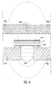
- Figure 4 corresponds to Figure 3 already described and shows, in section, the central part of a magnetic read head with two upper pole pieces 221, 222, an air gap 24, magnetic layers 311, 312 defining a second air gap 32 , a magnetoresistive element MR with its polarization conductor C.
- the head shown in FIG. 4 differs from that of FIG. 3 by the presence of an additional magnetic layer CM. It can be seen that the polarization field lines are channeled by the additional layer CM. The field lines are tightened in the area of the bias conductor, which reduces the leakage to the upper pole pieces 221, 222.
- FIG. 5 shows a magnetic read and write head which is of a known type (described in French patent application No. EN 93 13252 filed on November 8, 1993).
- This head is distinguished from the others by the fact that the magnetoresistive element MR extends from one pole piece 221 to the other 222.
- This element is connected to two contact pads 34, 36 located at the ends, these pads being themselves connected to means (not shown) capable of generating a current flowing in the magnetoresistive element MR.
- This element is, in this particular case, a multilayer material and its cross section is smaller than that of the upper pole pieces, in order to obtain a concentration effect of the reading field.
- the head of FIG. 5 is improved in its means for biasing the magnetoresistive element.
- These means include not only a polarization conductor C but also an additional magnetic layer CM.
- the additional magnetic layer is separated from the conductor C by an electrical and non-magnetic insulating layer I.
- This layer can be made of SiO2 or Si3N4 for example.
- FIG. 6 we can see, in section, an embodiment in which the magnetoresistive element assembly MR-polarization conductor C-additional magnetic layer CM is compact, the three elements being in contact with each other.
- the conductive element C has its face f1 in contact with the magnetoresistive element MR and its face f2 in contact with the magnetic layer CM.
- FIGS. 7a to 7c illustrate four stages of a particular embodiment of a magnetoresistive element and of its improved polarization means according to the invention.
- a substrate 50 for example made of silicon or ceramic (FIG. 7a).
- a layer of magnetoresistive material for example an alloy of iron, nickel, cobalt and / or a multilayer FeNi / Ag, is deposited on this substrate. This layer is etched to leave only the necessary ribbon MR.
- the width of the magnetoresistive element must be greater than that of the air gap. Take for example this width equal to 6 ⁇ m.
- An electrically conductive layer is then deposited, for example in CrAu, TiWAu, MoAu. We can proceed by cathode sputtering. This layer is etched in order to leave only contacts 52, 54 at each end of the magnetoresistive element (fig. 7b). A layer of non-magnetic and insulating material 56 is then deposited, for example made of SiO2 (fig. 7c). A conductive layer is then deposited, followed by a soft magnetic layer, for example by sputtering or vacuum evaporation. This layer can be an iron alloy, for example FeNi, Sendust (registered trademark) or a cobalt alloy, for example in CoZrNb. The thickness can be 0.2 ⁇ m. These two layers are engraved to give them the form of a ribbon.
- FIG. 8 illustrates a read and write head of the type which is described in the document FR-A-2 657 189 already cited.
- the substrate 10 the conductive winding 18 embedded in the insulator 20 as well as the pole pieces 221, 222 and the air gap 24 in the form of non-magnetic spacer 24, but no other pole piece.
- the magnetoresistive element MR is placed directly under the non-magnetic spacer 24.
- the polarization conductor C is placed under the element MR and the additional magnetic layer CM, specific to the invention, under the conductor C.
- the magnetic head shown in FIG. 9 differs from that of FIG. 8 only by the presence of a lower magnetic piece 14.
- FIG. 10 shows a head of a known type as illustrated in FIG. 2, but in which the magnetoresistive element assembly MR-polarization conductor C-additional magnetic layer CM is no longer placed above but in below the air gap 32.
Landscapes
- Engineering & Computer Science (AREA)
- Manufacturing & Machinery (AREA)
- Magnetic Heads (AREA)
Abstract
Description
- La présente invention a pour objet une tête magnétique de lecture à élément magnétorésistant et à moyens de polarisation perfectionnés.
- La tête de l'invention est avant tout une tête de lecture. Mais elle peut être équipée de moyens supplémentaires la rendant apte à une fonction d'écriture. L'invention trouve une application dans l'enregistrement magnétique ou dans la mesure des champs magnétiques.
- L'invention s'applique essentiellement aux têtes dites "horizontales à couches minces". Une telle tête est représentée sur la figure 1 annexée. On y voit un substrat semiconducteur 10, par exemple en silicium, dans lequel a été gravé un caisson 12. Dans ce caisson, une couche magnétique inférieure 14 a été formée électrolytiquement et a été prolongée par deux piliers verticaux 16₁, 16₂. Un bobinage 18 entoure ces piliers. Il est noyé dans une couche isolante 10. Le circuit magnétique se complète par deux pièces polaires supérieures 22₁, 22₂ séparées par un espaceur amagnétique 24 définissant l'entrefer de la tête. Un élément magnétorésistant MR, par exemple en fer-nickel, est disposé sous l'espaceur amagnétique 24. Cet élément est obtenu par photogravure, en prenant l'espaceur comme masque. Il est donc autoaligné par rapport à l'espaceur. Des moyens non représentés sont prévus pour faire passer un courant dans cet élément magnétorésistant MR et pour mesurer ses variations de résistance (variation de courant à tension constante ou vice versa). La tête se déplace devant un support magnétique 30 (bande, disque, ...) où sont enregistrées les informations à lire ou à écrire.
- Le fonctionnement d'une telle tête est schématiquement le suivant.
- A l'écriture, le courant circulant dans le bobinage 18 crée un champ magnétique et, par conséquent, une induction dans le circuit magnétique. Les lignes de champ qui s'épanouissent autour de l'espaceur induisent une aimantation dans le support 30.
- A la lecture, une information magnétique enregistrée dans le support 30 produit un champ magnétique de lecture et, par conséquent, une induction dans le circuit magnétique. Cette induction se referme, en partie, à travers l'élément magnétorésistant MR. Il en résulte une aimantation dans cet élément, qui va provoquer une variation de sa résistance.
- Une telle tête est décrite dans les documents FR-A-2 645 314 et FR-A-2 657 189.
- Un autre type de tête magnétique connu est illustré sur la figure 2. Cette tête comprend des éléments déjà représentés sur la figure 1 et qui portent les mêmes références numériques. La tête représentée se distingue de celle de la figure 1 par la présence de deux couches magnétiques 31₁, 31₂ écartées l'une de l'autre et en contact avec les pièces polaires supérieures. Ces couches définissent un autre entrefer 32, disposé sous l'entrefer principal 24. L'élément magnétorésistant MR est disposé à proximité et en travers de cet autre entrefer 32.
- Sur la figure 2 est représenté également un conducteur électrique C, qui sert de moyen de polarisation de l'élément magnétorésistant MR. Ce conducteur C est parcouru par un courant électrique dirigé perpendiculairement au plan de la figure. Le conducteur C présente une face f1 en regard de l'élément magnétorésistant MR et une face f2 opposée à cet élément.
- Une telle tête est décrite dans la demande de brevet français n°93 13249 déposée le 8 novembre 1993.
- D'autres têtes encore sont connues, comme celles qui sont divulguées par le document FR-A-2 657 189 déjà cité. Ces têtes présentent un circuit magnétique simplifié avec seulement deux pièces polaires supérieures, ou avec deux pièces polaires supérieures et une pièce polaire inférieure celle-ci étant sans contact avec les pièces polaires supérieures (cf figures 3 et 4 de ce document).
- Dans ces deux cas, il existe un élément magnétorésistant situé sous l'entrefer et un conducteur de polarisation parcouru par un courant.
- Dans tous ces cas, le courant circulant dans le conducteur de polarisation crée un champ magnétique qui se referme à travers l'élément magnétorésistant et qui se superpose au champ à lire. Le champ de polarisation est en général réglé pour que les variations de résistance de l'élément magnétorésistant soient linéaires en fonction des variations du champ à lire.
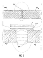
- Bien que donnant satisfaction à certains égards, ces têtes présentent un inconvénient. En effet, le champ magnétique créé par le courant circulant dans le conducteur de polarisation est capté par le circuit magnétique de la tête. Autrement dit, il a tendance à emprunter ce circuit magnétique pour se refermer. La figure 3 annexée montre les lignes de ce champ dans la zone des deux entrefers (l'entrefer principal 24 et l'autre entrefer 32) pour une tête connue conforme à celle de la figure 2. On voit que le champ passe, certes, dans l'élément magnétorésistant, mais qu'il emprunte aussi le circuit magnétique. Il va donc produire un champ parasite constant qui va entraîner une modification des informations enregistrées sur le support et apporter une asymétrie dans la forme du signal de lecture.
- L'invention a justement pour but de remédier à cet inconvénient.
- A cette fin, l'invention propose un perfectionnement des moyens de polarisation de l'élément magnétorésistant. Ce perfectionnement entraîne à la fois une baisse du courant nécessaire à la polarisation et une diminution du champ parasite créé dans l'entrefer.
- Ce but est atteint par l'utilisation d'une couche magnétique supplémentaire disposée sur le conducteur de polarisation, côté opposé à l'élément magnétorésistant. Cette couche a pour effet de canaliser le champ magnétique créé par le conducteur, champ qui, sans cette disposition, irait vers l'entrefer principal.
- Par ailleurs, le courant de détection qui parcourt l'élément magnétorésistant et qui sert à mesurer la variation de résistance de cet élément, crée lui aussi un champ magnétique, lequel sera également attiré par la couche magnétique supplémentaire. Il en résultera une augmentation de l'aimantation de cette couche et, en conséquence et par effet miroir, une augmentation de la polarisation de l'élément magnétorésistant. L'effet produit par l'adjonction de la couche magnétique est donc doublement bénéfique.
- Grâce à l'invention, on peut ainsi diminuer le courant de polarisation d'environ 20%, ce qui réduit d'autant les pertes JOULE et l'échauffement de la tête. Le fait que la couche magnétique soit en contact avec la couche conductrice augmente encore l'efficacité de la disposition.
- La couche magnétique supplémentaire est de préférence réalisée en un matériau magnétique doux. Il peut s'agir d'alliages à base de fer, comme le fernickel ou le Sendust (marque déposée) qui est un alliage de 85% de fer, 5,4% d'aluminium et 9,6% de silicium en masse, ou bien d'alliages à base de cobalt comme l'alliage cobalt-zirconium-niobium. Son épaisseur peut être comprise entre 100 et 500 nm, de préférence voisine de 200 nm. Sa largeur est sensiblement égale à la largeur du conducteur de polarisation. La présence de cette couche magnétique supplémentaire ne complique pas le procédé de réalisation de la tête puisque l'ensemble conducteur-couche magnétique peut être réalisé en une seule gravure.
- L'invention peut s'appliquer à n'importe quelles têtes de lecture, notamment à celles qui ont été décrites plus haut, où à celles à venir qui utiliseront un élément magnétorésistant et un conducteur de polarisation.
-
- la figure 1, déjà décrite, montre une tête horizontale connue à élément magnétorésistant ;
- la figure 2, déjà décrite, montre une autre tête magnétique à élément magnétorésistant et à conducteur de polarisation ;
- la figure 3, déjà décrite, montre les lignes de champ magnétique de polarisation dans une tête telle que celle de la figure précédente ;
- la figure 4 montre la nouvelle répartition des lignes de champ dans le cas de l'invention ;
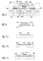
- la figure 5 montre une tête magnétique d'un type connu à élément magnétorésistant longitudinal, perfectionnée selon l'invention ;
- la figure 6 est une coupe illustrant un mode de réalisation compact de l'ensemble élément magnétorésistant-conducteur de polarisation-couche magnétique supplémentaire ;
- les figures 7a à 7c montrent diverses étapes d'un procédé de réalisation de l'ensemble élément magnétorésistant-conducteur de polarisation-couche magnétique supplémentaire ;
- la figure 8 montre encore une autre tête magnétique d'un type connu perfectionnée selon l'invention ;
- la figure 9 montre encore une autre tête magnétique d'un type connu perfectionnée selon l'invention ;
- la figure 10 illustre un mode de réalisation où la magnétorésistance et ses moyens de polarisation sont situés sous le second entrefer.
- La figure 4 correspond à la figure 3 déjà décrite et montre, en coupe, la partie centrale d'une tête magnétique de lecture avec deux pièces polaires supérieures 22₁, 22₂, un entrefer 24, des couches magnétiques 31₁, 31₂ définissant un second entrefer 32, un élément magnétorésistant MR avec son conducteur de polarisation C. La tête représentée sur la figure 4 se distingue de celle de la figure 3 par la présence d'une couche magnétique supplémentaire CM. On voit que les lignes de champ de polarisation sont canalisées par la couche supplémentaire CM. Les lignes de champ sont resserrées dans la zone du conducteur de polarisation, ce qui réduit la fuite vers les pièces polaires supérieures 22₁, 22₂.
- La figure 5 montre une tête magnétique de lecture et d'écriture qui est d'un type connu (décrit dans la demande de brevet français n° EN 93 13252 déposée le 8 novembre 1993). Cette tête se distingue des autres par le fait que l'élément magnétorésistant MR s'étend d'une pièce polaire 22₁ à l'autre 22₂. Cet élément est relié à deux plots de contact 34, 36 situés aux extrémités, ces plots étant eux-mêmes reliés à des moyens (non représentés) aptes à engendrer un courant circulant dans l'élément magnétorésistant MR. Cet élément est, dans ce cas particulier, un matériau multicouche et sa section droite est inférieure à celle des pièces polaires supérieures, afin d'obtenir un effet de concentration du champ de lecture.
- La tête de la figure 5 est perfectionnée dans ses moyens de polarisation de l'élément magnétorésistant. Ces moyens comprennent non seulement un conducteur de polarisation C mais aussi une couche magnétique supplémentaire CM. Dans la variante illustrée, la couche magnétique supplémentaire est séparée du conducteur C par une couche isolante électrique et amagnétique I. Cette couche peut être en SiO₂ ou en Si₃N₄ par exemple.
- Sur la figure 6, on voit, en coupe, un mode de réalisation dans lequel l'ensemble élément magnétorésistant MR-conducteur de polarisation C-couche magnétique supplémentaire CM est compact, les trois éléments étant en contact les uns avec les autres. L'élément conducteur C a sa face f1 en contact avec l'élément magnétorésistant MR et sa face f2 en contact avec la couche magnétique CM.
- Les figures 7a à 7c illustrent quatre étapes d'un mode particulier de réalisation d'un élément magnétorésistant et de ses moyens de polarisation perfectionnés selon l'invention.
- On part d'un substrat 50, par exemple en silicium ou en céramique (fig. 7a). On dépose sur ce substrat une couche en matériau magnétorésistant, par exemple en alliage de fer, nickel, cobalt et/ou en multicouche FeNi/Ag. On grave cette couche pour ne laisser subsister que le ruban nécessaire MR. La largeur de l'élément magnétorésistant doit être supérieure à celle de l'entrefer. On prendra par exemple cette largeur égale à 6 µm.
- On dépose ensuite une couche électriquement conductrice par exemple en CrAu, TiWAu, MoAu. On peut procéder par pulvérisation cathodique. On grave cette couche pour ne laisser subsister que des contacts 52,54 à chaque extrémité de l'élément magnétorésistant (fig. 7b). On dépose ensuite une couche de matériau isolant et amagnétique 56, par exemple en SiO₂ (fig. 7c). On dépose ensuite une couche conductrice puis une couche magnétique douce, par exemple par pulvérisation cathodique ou évaporation sous vide. Cette couche peut être un alliage de fer, par exemple en FeNi, en Sendust (marque déposée) ou en alliage de cobalt, par exemple en CoZrNb. L'épaisseur peut être de 0,2 µm. On grave ces deux couches pour leur donner la forme d'un ruban.
- On poursuit la réalisation de la tête comme décrit dans les documents cités plus haut. Si l'on ne désire qu'une tête de lecture, on ne formera pas de bobinage conducteur autour du circuit magnétique. Si l'on veut obtenir une tête de lecture et d'écriture un tel bobinage devra être constitué.
- La figure 8 illustre une tête de lecture et d'écriture du type de celle qui est décrite dans le document FR-A-2 657 189 déjà cité. On y retrouve le substrat 10, le bobinage conducteur 18 noyé dans l'isolant 20 ainsi que les pièces polaires 22₁, 22₂ et l'entrefer 24 sous forme d'espaceur amagnétique 24, mais aucune autre pièce polaire. L'élément magnétorésistant MR est placé directement sous l'espaceur amagnétique 24. Le conducteur de polarisation C est placé sous l'élément MR et la couche magnétique supplémentaire CM, propre à l'invention, sous le conducteur C.
- La tête magnétique représentée sur la figure 9 ne diffère de celle de la figure 8 que par la présence d'une pièce magnétique inférieure 14.
- Enfin, la figure 10 montre une tête d'un type connu tel qu'illustré sur la figure 2, mais dans laquelle l'ensemble élément magnétorésistant MR-conducteur de polarisation C-couche magnétique supplémentaire CM est placé non plus au-dessus mais en dessous de l'entrefer 32.
Claims (13)
cette tête magnétique étant caractérisée par le fait que les moyens de polarisation comprennent en outre une couche magnétique supplémentaire (CM) disposée sur le conducteur de polarisation (C), côté face opposée (f2) à l'élément magnétorésistant (MR).
Applications Claiming Priority (2)
| Application Number | Priority Date | Filing Date | Title |
|---|---|---|---|
| FR9402258A FR2716741B1 (fr) | 1994-02-28 | 1994-02-28 | Tête magnétique de lecture à élément magnétorésistant et à moyens de polarisation perfectionnés. |
| FR9402258 | 1994-02-28 |
Publications (3)
| Publication Number | Publication Date |
|---|---|
| EP0669609A2 true EP0669609A2 (fr) | 1995-08-30 |
| EP0669609A3 EP0669609A3 (fr) | 1995-10-18 |
| EP0669609B1 EP0669609B1 (fr) | 2001-08-08 |
Family
ID=9460489
Family Applications (1)
| Application Number | Title | Priority Date | Filing Date |
|---|---|---|---|
| EP95400409A Expired - Lifetime EP0669609B1 (fr) | 1994-02-28 | 1995-02-27 | Tête magnétique de lecture à élément magnétorésistant et à moyens de polarisation perfectionnés |
Country Status (5)
| Country | Link |
|---|---|
| US (1) | US5798895A (fr) |
| EP (1) | EP0669609B1 (fr) |
| JP (1) | JPH07262528A (fr) |
| DE (1) | DE69522022T2 (fr) |
| FR (1) | FR2716741B1 (fr) |
Families Citing this family (1)
| Publication number | Priority date | Publication date | Assignee | Title |
|---|---|---|---|---|
| FR2761477B1 (fr) * | 1997-04-01 | 1999-04-23 | Commissariat Energie Atomique | Capteur de champ magnetique a magnetoresistance |
Family Cites Families (21)
| Publication number | Priority date | Publication date | Assignee | Title |
|---|---|---|---|---|
| JPS56165923A (en) * | 1980-05-24 | 1981-12-19 | Matsushita Electric Ind Co Ltd | Magnetic head |
| JPS57203226A (en) * | 1981-06-09 | 1982-12-13 | Mitsubishi Electric Corp | Thin film magnetic reluctance head |
| JPS5971118A (ja) * | 1982-10-14 | 1984-04-21 | Matsushita Electric Ind Co Ltd | 垂直磁化再生ヘツド |
| JPS58185019A (ja) * | 1982-04-21 | 1983-10-28 | Hitachi Ltd | 磁気抵抗効果型ヘツド |
| JPS60157712A (ja) * | 1984-01-26 | 1985-08-19 | Sony Corp | 磁気抵抗効果型磁気ヘツド |
| JPS61134913A (ja) * | 1984-12-05 | 1986-06-23 | Matsushita Electric Ind Co Ltd | 磁気抵抗型薄膜ヘツド |
| JPS6258411A (ja) * | 1985-09-09 | 1987-03-14 | Sony Corp | 磁気抵抗効果型磁気ヘツド |
| JPS62102411A (ja) * | 1985-10-29 | 1987-05-12 | Victor Co Of Japan Ltd | 磁気抵抗効果ヘツド |
| US5225951A (en) * | 1985-12-27 | 1993-07-06 | Sharp Kabushiki Kaisha | Thin film magnetic head with reduced internal stresses |
| US5159511A (en) * | 1987-04-01 | 1992-10-27 | Digital Equipment Corporation | Biasing conductor for MR head |
| JPS6413209A (en) * | 1987-07-03 | 1989-01-18 | Kansai Nippon Electric | Yoke type thin film magnetic head |
| JPH01145520A (ja) * | 1987-12-01 | 1989-06-07 | Yaskawa Electric Mfg Co Ltd | アブソリュート磁気エンコーダ |
| US4881143A (en) * | 1988-01-19 | 1989-11-14 | Hewlett-Packard Company | Compensated magneto-resistive read head |
| JPH02187911A (ja) * | 1989-01-13 | 1990-07-24 | Matsushita Electric Ind Co Ltd | 磁気抵抗効果型ヘッド |
| JP2728487B2 (ja) * | 1989-02-08 | 1998-03-18 | 株式会社日立製作所 | 録再分離複合型磁気ヘッド |
| FR2657189B1 (fr) * | 1990-01-18 | 1993-12-31 | Commissariat A Energie Atomique | Tete magnetique de lecture et d'ecriture a element magnetoresistant. |
| US5274521A (en) * | 1990-08-23 | 1993-12-28 | Sony Corporation | Planar thin film magnetic head |
| JP3200060B2 (ja) * | 1990-09-12 | 2001-08-20 | ソニー株式会社 | 薄膜磁気ヘッド |
| JPH05114119A (ja) * | 1991-10-21 | 1993-05-07 | Fujitsu Ltd | 磁気抵抗効果型磁気ヘツド |
| US5255141A (en) * | 1991-12-16 | 1993-10-19 | Read-Rite Corp. | Read-write magnetic head with flux sensing read element |
| JPH05182146A (ja) * | 1992-01-08 | 1993-07-23 | Sumitomo Metal Ind Ltd | 薄膜磁気ヘッド |
-
1994
- 1994-02-28 FR FR9402258A patent/FR2716741B1/fr not_active Expired - Fee Related
-
1995
- 1995-02-27 JP JP7061613A patent/JPH07262528A/ja active Pending
- 1995-02-27 EP EP95400409A patent/EP0669609B1/fr not_active Expired - Lifetime
- 1995-02-27 DE DE69522022T patent/DE69522022T2/de not_active Expired - Fee Related
-
1997
- 1997-01-29 US US08/792,707 patent/US5798895A/en not_active Expired - Fee Related
Also Published As
| Publication number | Publication date |
|---|---|
| EP0669609B1 (fr) | 2001-08-08 |
| FR2716741A1 (fr) | 1995-09-01 |
| JPH07262528A (ja) | 1995-10-13 |
| US5798895A (en) | 1998-08-25 |
| DE69522022T2 (de) | 2002-03-28 |
| FR2716741B1 (fr) | 1996-04-05 |
| EP0669609A3 (fr) | 1995-10-18 |
| DE69522022D1 (de) | 2001-09-13 |
Similar Documents
| Publication | Publication Date | Title |
|---|---|---|
| EP0284495B1 (fr) | Tête magnétique de lecture pour piste de très faible largeur et procédé de fabrication | |
| EP0418372B1 (fr) | Tete magnetique de lecture a magnetoresistance pour enregistrement perpendiculaire et procede de realisation d'une telle tete | |
| KR100295289B1 (ko) | 후방자속가이드로서의감지층을갖는자기터널접합부자기저항판독헤드 | |
| KR100271142B1 (ko) | 자속 가이드로서의 감지층을 갖는 자기 터널 접합부 자기 저항판독 헤드 | |
| EP0420755B1 (fr) | Procédé de réalisation d'une tête d'enregistrement magnétique et tête obtenue par ce procédé | |
| EP0438350B1 (fr) | Tête magnétique de lecture et d'écriture à élément magnétorésistant | |
| FR2645314A1 (fr) | Tete magnetique a magnetoresistance pour enregistrement longitudinal et procede de realisation d'une telle tete | |
| EP0693791A1 (fr) | Capteur à magnétorésistance multicouche autopolarisée | |
| EP0702358A1 (fr) | Tête magnétique à magnétorésistance multicouche longitudinale sous-jacente | |
| EP0781448B1 (fr) | Tete magnetique planaire a magnetoresistance multicouche longitudinale | |
| FR2817622A1 (fr) | Micromagnetometre a porte de flux | |
| FR2700633A1 (fr) | Procédé de réalisation d'une tête magnétique à détecteur de champ à semiconducteur et tête obtenue par ce procédé. | |
| EP0642181B1 (fr) | Composant et capteur magnétorésistifs à motif géométrique répété | |
| EP0642030A1 (fr) | Guide de flux magnétique à languettes et capteur magnétorésistif comportant ce guide | |
| EP0497069B1 (fr) | Procédé de fabrication de capteurs magnéto-résistifs, et dispositif magnétique réalisé suivant un tel procédé | |
| FR2648941A1 (fr) | Tete de lecture magnetique a effet hall | |
| EP0669609B1 (fr) | Tête magnétique de lecture à élément magnétorésistant et à moyens de polarisation perfectionnés | |
| EP0644528B1 (fr) | Tête magnétique de lecture et d'écriture à élément magnétorésistant compensé en écriture | |
| EP1023608B1 (fr) | Capteur de champ magnetique a magnetoresistance | |
| EP0694909B1 (fr) | Tête magnétique à élément saturable et dispositif matriciel comportant un ensemble de têtes magnétiques | |
| FR2802011A1 (fr) | Tete de lecture planaire a element magneto-resistif | |
| FR2676301A1 (fr) | Tete magnetique d'ecriture et de lecture a largeur de poles dissymetrique. | |
| FR2713782A1 (fr) | Capteur magnétique à effet magnéto-résistif. | |
| FR2769399A1 (fr) | Tete magnetique avec une partie lecture et une partie ecriture | |
| FR2744554A1 (fr) | Tete magnetique a element magnetoresistant enterre dans l'entrefer et procede de realisation |
Legal Events
| Date | Code | Title | Description |
|---|---|---|---|
| PUAI | Public reference made under article 153(3) epc to a published international application that has entered the european phase |
Free format text: ORIGINAL CODE: 0009012 |
|
| PUAL | Search report despatched |
Free format text: ORIGINAL CODE: 0009013 |
|
| AK | Designated contracting states |
Kind code of ref document: A2 Designated state(s): DE FR GB IT |
|
| AK | Designated contracting states |
Kind code of ref document: A3 Designated state(s): DE FR GB IT |
|
| 17P | Request for examination filed |
Effective date: 19960314 |
|
| 17Q | First examination report despatched |
Effective date: 19981109 |
|
| GRAG | Despatch of communication of intention to grant |
Free format text: ORIGINAL CODE: EPIDOS AGRA |
|
| GRAG | Despatch of communication of intention to grant |
Free format text: ORIGINAL CODE: EPIDOS AGRA |
|
| GRAH | Despatch of communication of intention to grant a patent |
Free format text: ORIGINAL CODE: EPIDOS IGRA |
|
| GRAH | Despatch of communication of intention to grant a patent |
Free format text: ORIGINAL CODE: EPIDOS IGRA |
|
| GRAA | (expected) grant |
Free format text: ORIGINAL CODE: 0009210 |
|
| AK | Designated contracting states |
Kind code of ref document: B1 Designated state(s): DE FR GB IT |
|
| REF | Corresponds to: |
Ref document number: 69522022 Country of ref document: DE Date of ref document: 20010913 |
|
| GBT | Gb: translation of ep patent filed (gb section 77(6)(a)/1977) |
Effective date: 20011102 |
|
| REG | Reference to a national code |
Ref country code: GB Ref legal event code: IF02 |
|
| PLBE | No opposition filed within time limit |
Free format text: ORIGINAL CODE: 0009261 |
|
| STAA | Information on the status of an ep patent application or granted ep patent |
Free format text: STATUS: NO OPPOSITION FILED WITHIN TIME LIMIT |
|
| 26N | No opposition filed | ||
| PGFP | Annual fee paid to national office [announced via postgrant information from national office to epo] |
Ref country code: DE Payment date: 20030223 Year of fee payment: 9 |
|
| PGFP | Annual fee paid to national office [announced via postgrant information from national office to epo] |
Ref country code: FR Payment date: 20030225 Year of fee payment: 9 |
|
| PGFP | Annual fee paid to national office [announced via postgrant information from national office to epo] |
Ref country code: GB Payment date: 20030226 Year of fee payment: 9 |
|
| PG25 | Lapsed in a contracting state [announced via postgrant information from national office to epo] |
Ref country code: GB Free format text: LAPSE BECAUSE OF NON-PAYMENT OF DUE FEES Effective date: 20040227 |
|
| PG25 | Lapsed in a contracting state [announced via postgrant information from national office to epo] |
Ref country code: DE Free format text: LAPSE BECAUSE OF NON-PAYMENT OF DUE FEES Effective date: 20040901 |
|
| GBPC | Gb: european patent ceased through non-payment of renewal fee | ||
| PG25 | Lapsed in a contracting state [announced via postgrant information from national office to epo] |
Ref country code: FR Free format text: LAPSE BECAUSE OF NON-PAYMENT OF DUE FEES Effective date: 20041029 |
|
| REG | Reference to a national code |
Ref country code: FR Ref legal event code: ST |
|
| PG25 | Lapsed in a contracting state [announced via postgrant information from national office to epo] |
Ref country code: IT Free format text: LAPSE BECAUSE OF NON-PAYMENT OF DUE FEES;WARNING: LAPSES OF ITALIAN PATENTS WITH EFFECTIVE DATE BEFORE 2007 MAY HAVE OCCURRED AT ANY TIME BEFORE 2007. THE CORRECT EFFECTIVE DATE MAY BE DIFFERENT FROM THE ONE RECORDED. Effective date: 20050227 |