EP0671601A2 - System und Verfahren für optisches interferometrisches Messen - Google Patents
System und Verfahren für optisches interferometrisches Messen Download PDFInfo
- Publication number
- EP0671601A2 EP0671601A2 EP95102557A EP95102557A EP0671601A2 EP 0671601 A2 EP0671601 A2 EP 0671601A2 EP 95102557 A EP95102557 A EP 95102557A EP 95102557 A EP95102557 A EP 95102557A EP 0671601 A2 EP0671601 A2 EP 0671601A2
- Authority
- EP
- European Patent Office
- Prior art keywords
- beams
- frequency
- measuring
- polarized
- difference
- Prior art date
- Legal status (The legal status is an assumption and is not a legal conclusion. Google has not performed a legal analysis and makes no representation as to the accuracy of the status listed.)
- Ceased
Links
Images


Classifications
-
- G—PHYSICS
- G01—MEASURING; TESTING
- G01B—MEASURING LENGTH, THICKNESS OR SIMILAR LINEAR DIMENSIONS; MEASURING ANGLES; MEASURING AREAS; MEASURING IRREGULARITIES OF SURFACES OR CONTOURS
- G01B9/00—Measuring instruments characterised by the use of optical techniques
- G01B9/02—Interferometers
- G01B9/02015—Interferometers characterised by the beam path configuration
- G01B9/02017—Interferometers characterised by the beam path configuration with multiple interactions between the target object and light beams, e.g. beam reflections occurring from different locations
- G01B9/02019—Interferometers characterised by the beam path configuration with multiple interactions between the target object and light beams, e.g. beam reflections occurring from different locations contacting different points on same face of object
-
- G—PHYSICS
- G01—MEASURING; TESTING
- G01B—MEASURING LENGTH, THICKNESS OR SIMILAR LINEAR DIMENSIONS; MEASURING ANGLES; MEASURING AREAS; MEASURING IRREGULARITIES OF SURFACES OR CONTOURS
- G01B11/00—Measuring arrangements characterised by the use of optical techniques
- G01B11/30—Measuring arrangements characterised by the use of optical techniques for measuring roughness or irregularity of surfaces
- G01B11/303—Measuring arrangements characterised by the use of optical techniques for measuring roughness or irregularity of surfaces using photoelectric detection means
-
- G—PHYSICS
- G01—MEASURING; TESTING
- G01B—MEASURING LENGTH, THICKNESS OR SIMILAR LINEAR DIMENSIONS; MEASURING ANGLES; MEASURING AREAS; MEASURING IRREGULARITIES OF SURFACES OR CONTOURS
- G01B9/00—Measuring instruments characterised by the use of optical techniques
- G01B9/02—Interferometers
- G01B9/02001—Interferometers characterised by controlling or generating intrinsic radiation properties
- G01B9/02002—Interferometers characterised by controlling or generating intrinsic radiation properties using two or more frequencies
- G01B9/02003—Interferometers characterised by controlling or generating intrinsic radiation properties using two or more frequencies using beat frequencies
-
- G—PHYSICS
- G01—MEASURING; TESTING
- G01B—MEASURING LENGTH, THICKNESS OR SIMILAR LINEAR DIMENSIONS; MEASURING ANGLES; MEASURING AREAS; MEASURING IRREGULARITIES OF SURFACES OR CONTOURS
- G01B9/00—Measuring instruments characterised by the use of optical techniques
- G01B9/02—Interferometers
- G01B9/02015—Interferometers characterised by the beam path configuration
- G01B9/02027—Two or more interferometric channels or interferometers
- G01B9/02028—Two or more reference or object arms in one interferometer
-
- G—PHYSICS
- G01—MEASURING; TESTING
- G01B—MEASURING LENGTH, THICKNESS OR SIMILAR LINEAR DIMENSIONS; MEASURING ANGLES; MEASURING AREAS; MEASURING IRREGULARITIES OF SURFACES OR CONTOURS
- G01B2290/00—Aspects of interferometers not specifically covered by any group under G01B9/02
- G01B2290/30—Grating as beam-splitter
-
- G—PHYSICS
- G01—MEASURING; TESTING
- G01B—MEASURING LENGTH, THICKNESS OR SIMILAR LINEAR DIMENSIONS; MEASURING ANGLES; MEASURING AREAS; MEASURING IRREGULARITIES OF SURFACES OR CONTOURS
- G01B2290/00—Aspects of interferometers not specifically covered by any group under G01B9/02
- G01B2290/45—Multiple detectors for detecting interferometer signals
-
- G—PHYSICS
- G01—MEASURING; TESTING
- G01B—MEASURING LENGTH, THICKNESS OR SIMILAR LINEAR DIMENSIONS; MEASURING ANGLES; MEASURING AREAS; MEASURING IRREGULARITIES OF SURFACES OR CONTOURS
- G01B2290/00—Aspects of interferometers not specifically covered by any group under G01B9/02
- G01B2290/70—Using polarization in the interferometer
Definitions
- This invention relates generally to a surface roughness optical measuring apparatus and method and in particular to optically measuring on-line the surface roughness of a product during the manufacturing process.
- optical interferometry has been known and studied for many years.
- optical interferometry involves creating a beam of light which is split into a measuring beam and a reference beam so that the measuring beam is reflected off of the test item and the reference beam is reflected off of a fixed object, the two beams are recombined, and an interference or fringe pattern is created which is proportional to the phase difference imparted on the measuring beam by the surface of the test object.
- Monochromatic coherent light allows for greater accuracy and sensitivity in determining minute variations in measuring parameters such as indices of refraction, phase, amplitude, and polarity.
- the technique disclosed in the Laub patent is inefficient due to waste of the output light and because only a small portion of the area of beam incidence between the overlapping spots is usable to detect the phase displacement, or shear, between the frequency differentiated measuring beams. Furthermore, variability in the ramp generator to the acousto-optical modulator leads to fluctuations in the distance between optical centers of the two measuring beams. This will artificially introduce phase differences as the beam centers shift away from and toward each other.
- the Laub method is subject to temperature and vibrational contamination as well as fluctuations that may be caused by changes in the focal length and out of focus measurements.
- This apparatus is less susceptible to vibration as compared to a single Michelson interferometer but it does not eliminate vibrational noise because of its reliance on a separate stationary reference beam to create the interference.
- Other difficulties with this apparatus relate to the use of two or more beams differentiated by frequency, which requires intervening electronic switching between measurements from one beam to the next.
- a third example of a multiple beam interferometer is disclosed in U.S. Patent No. 5,139,336 issued to See et al. on August 18, 1992.
- the patent discloses a heterodyned interferometer using amplitude modulation as well as different frequencies between the two measuring beams.
- the device either uses a zero order and one first-order beam for measuring a surface or it incorporates at least two driving frequencies for a Bragg cell acousto-optical modulator to create two first-order beams of different frequency. In either case the measuring beams undergo amplitude modulation. As disclosed, this device is affected by surface color and reflectivity changes.
- the invention discloses a method and system for measuring surface characteristics of a specimen while that specimen is moving or in a manufacturing process.
- the invention is adaptable to numerous manufacturing processes that use on-line surface characteristic monitoring to control the quality and quantity of the products generated by that manufacturing process.
- the present invention makes use of a twin or dual beam heterodyned optical interferometer coupled to a manufacturing process to accomplish the surface characteristic monitoring.
- the twin or dual beam heterodyned optical interferometer is designed to minimize interference and background noise due to changes in signal amplitude, color, surface chemistry, surface vibration, surface motion, and degradation of signal due to beam focus discrepancies. All of these limitations are minimized through the use of two monochromatic coherent radiant energy beams directed onto the surface to be measured, the two beams being distinguishable by the polarity difference between them. In this way the two beams act as a reference to each other with the change imposed on the beams by the interaction of the two beams with the surface detectable as a phase shift relative to the two beams. The phase shift detected between the two beams is equated to a surface characteristic through the use of statistical analysis performed on the phase shift change data.
- Results of the statistical analysis are used to control manufacturing process parameters in a feedback control fashion at various stages of a manufacturing process.
- High speed integrated computer hardware and software programming allows for rapid feedback control of a manufacturing process using optical interferometry as a monitoring tool.
- the computer interface also allows detection of abrupt or large changes in the phase shift between the two beams which signifies gross errors or defects in the surface undergoing measurement. Data collected in this fashion is useful as a quality assessment parameter for the manufacturing process.
- Another application of the invention is the on-line monitoring of fine motion attributes of an object.
- the invention would yield information representative of the object's motion consistent with changes in pitch and roll.
- Figure 1 is a schematic representation of an embodiment of a twin beam heterodyned laser interferometer.
- Figure 2 is a schematic representation of the interaction of the twin beams on a surface of a moving object at time T1.
- Figure 3 is a schematic representation of the interaction of the twin beams on a surface of a moving object at time T2.
- Figure 4 is a schematic representation of the interaction of the twin beams on a surface of a moving object at time T3.
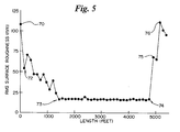
- Figure 5 is a graphic representation of statistical data received by a twin beam laser interferometer.
- Figure 6 is a schematic representation of another embodiment of the present invention depicting a dual beam heterodyned laser interferometer.
- Figure 7 is a schematic representation of a manufacturing process for magnetic media depicting on-line laser interferometer measurements of surface roughness and using the data collected to control the manufacturing process.
- Figure 1 discloses a twin beam heterodyned interferometer comprising laser source 20, acousto-optic modulator 22, frequency oscillator 24, refracting polarizer 26, focusing lens 28, polarizing beam splitter 36, photodetectors 42 and 44, comparator 46, computer 48, and manufacturing process control interface 50.
- Laser source 20 provides a coherent monochromatic output light beam 21 of frequency f 0.
- Light beam 21 enters acousto-optic modulator 22.
- Acousto-optic modulator 22 uses an optical medium that is vibrated mechanically by a piezoelectric crystal driven by the output from frequency oscillator 24 at frequency f m .
- the mechanical vibrations traverse the optical medium of acousto-optic modulator 22 perpendicular to the optical path of light beam 21.
- the vibration of the optical medium of acousto-optic modulator 22 creates a diffraction grating, diffracting light beam 21.
- frequency oscillator 24 provides a 40 MHz output, although a wide range of frequencies are available.
- the effect of acousto-optic modulator 22 is to create a zero order beam 23 and multiple n th order beams.
- the resultant zero order beam 23 is identical, except for amplitude, to the laser output light beam 21.
- a first-order output beam 25 is frequency shifted by an amount f m to f1 which in the present embodiment is equal to f 0 plus 40 MHz and is diffracted off axis from zero order beam 23 by angle ⁇ .
- the present invention uses the zero order beam and one of the first-order beams.
- First-order light beam 25 from acousto-optic modulator 22 is directed to refracting polarizer 26, which is a Wollaston prism in the present embodiment.
- Refracting polarizer 26 creates two diverging orthogonal linearly polarized light measuring beams 30 and 32.
- Focusing lens 28 focuses the divergent polarized measuring beams 30 and 32 onto two separate sites of surface 34, which is the surface to be measured. Focusing of the two polarized measuring beams 30 and 32 ensures the smallest spot size possible at each site, as well as the brightest spot, to maximize the amount of light reflected from surface 34 back along the paths of each polarized measuring beams 30 and 32. Since polarized measuring beams 30 and 32 are incident with surface 34 at separate sites, the optical path lengths of these two orthogonal linearly polarized beams are different. The path length difference information is proportional to the phase change between the two measuring beams 30 and 32.
- Reflected measuring beams 30 and 32 travel the reverse path of original beams 30 and 32. Since only the light reflected back along the original light path of beams 30 and 32 is used, some light intensity is lost due to scattering effects of surface 34. Measuring beams 30 and 32 are converged at lens 28 and refracting polarizer 26, and are recombined into a single measuring beam 27 of frequency f 1 along a path back to acousto-optic modulator 22. Alternate means for collecting the polarized beams reflected from the surface of the object include use of a lens, prism, mirror, or even a retroreflective device.
- measuring beam 27 is diffracted and frequency shifted in acousto-optic modulator 22 by an amount equal to the frequency output of frequency oscillator 24. Then, the portion of the beam emerging from acousto-optic modulator 22 in the reverse path is a measuring beam 29 and is now frequency shifted twice f m to f 2, which in the present embodiment is f0 plus 80 MHz. Measuring light beam 29 travels in the reverse direction of beam 21 back to an output mirror or reflective surface at the forward end of laser 20.
- measuring beam 29 is superimposed with f0 light in light beam 21 from laser 20.
- This superimposition of f 2 light with f0 light sets up an interference with a beat frequency of twice f m , or 80 MHz.
- Polarizing beam splitter 36 is aligned to receive the emerging zero order beam 23 of frequency f0 and zero order beams 29 of frequency f 2.
- Polarizing beam splitter 36 splits beams 23 and 29 into orthogonal linearly polarized beams 38 and 40 emerging from polarizing beam splitter 36 substantially at right angles to each other.
- Polarized beams 38 and 40 carry their respective polarized components from beams 30 and 32, but at frequency f 2.
- the orthogonal linearly polarized components of beam 23 provide the beat frequency interference that can be detected.
- Photodetectors 42 and 44 detect beams 38 and 40 and the outputs of detectors 42 and 44 are sent to comparator 46.
- Comparator 46 uses an analog to digital converter to translate the two beat frequency beams into digital format to carry out the comparison of the beams.
- the phase shift imposed upon beams 30 and 32 by the surface irregularities of surface 34 are represented in the phase shift calculated by comparator 46 between the beat frequencies of beams 38 and 40.
- Figures 2-4 schematically depict measuring beams 30 and 32 incident to surface 34, which is moving in the direction of arrow 47.
- Difference in surface height, or asperity causes a difference in path length between measuring beams 30 and 32. This path length is proportional to twice the actual height asperity, or ⁇ Z.
- measuring beam 30 is incident at surface site 52 and measuring beam 32 is incident at surface site 54.
- the actual surface height difference is equivalent to ⁇ Z(t1).
- Measuring beam 32 must travel twice the distance ⁇ Z(t1), and the phase change ⁇ imparted on measuring beam 32 will be proportional to 2 ⁇ Z(t1).
- measuring beams 30 and 32 are now incident at two new sites 56 and 58 separated in height by ⁇ Z(t2).
- the path length for measuring beam 30 is now longer by 2 ⁇ Z(t2) which will lead to a relative phase change in the opposite direction from the phase change detected at time t1.
- the system is able to track the phase change through the four quadrants of the unit circle. If a ⁇ Z(t) increases beyond 1/2 ⁇ of the light, the ⁇ values repeat as a function of the unit circle in trigonometric functions.
- the invention tracks ⁇ changes through the four quadrants of a unit circle, keeping track of the number of occurrences of apparent phase reversal.
- ⁇ Z's such as the example shown in time frame t3, depicted in Figure 4, are accurately detected as multiples of 2 ⁇ as the path of measuring beam 30 lengthens over the distance from site 56 to site 60 and the path of measuring beam 32 shortens over the distance from site 58 to site 62.
- a calculation of phase shift as a function of path length difference is accomplished electronically by a quadrature phase demodulator circuitry within comparator 46.
- A is signal amplitude from detector 42
- B signal amplitude from detector 44
- ⁇ is the radial frequency of the signals
- t time
- ⁇ a (t) is the time dependent phase shift of signal 1
- ⁇ b (t) is the time dependent phase shift of signal 2.
- Signal 1 is processed by a power splitter into signals 3 and 4 which are identical except for decreased signal amplitude: eq. 3
- Signal 3 A' sin ( ⁇ t + ⁇ a (t)), and eq. 4
- Signal 4 A' sin ( ⁇ t + ⁇ a (t)).
- Signals 3 and 6 are sent to one mixer and signals 4 and 5 are sent to a second mixer.
- the mixed signals are filtered through a low pass filter yielding:
- Signals 7 and 8 are digitized by an A/D converter in comparator 46 and sent to computer 48.
- Computer 48 divides signal 8 by signal 7 yielding: Notice that the amplitude coefficients cancel out.
- the expression ( ⁇ a (t) - ⁇ b (t)) is equivalent to ⁇ (t), which is proportional to 2 ⁇ Z representing the beam path length difference between measuring beams 30 and 32.
- Substituting and solving for ⁇ Z yields the following equation: where ⁇ is the wavelength of the light used, and ⁇ Z(t) is the time dependent height difference between the laser illuminated spots.
- the computer also keeps track of which quadrant of the unit circle each measuring point is in and is able to effectively demodulate phase differences greater than 2 ⁇ .
- Phase shift data from comparator 46 is fed to computer 48 for statistical analysis of the phase shift changes as surface 34 moves past measuring beams 30 and 32.
- the phase shift information is then utilized by computer 48 to effect feedback control to the manufacturing process to keep the production process within the parameters set for the product.
- Figure 5 is a graphic representation of data obtained by use of the invention during a manufacturing process.
- a plastic sheet in the form of a web is coated with a magnetic material to create a magnetic storage tape.
- the clarity of an audio or video signal reproduction obtainable from a magnetic tape is inversely proportional to the surface roughness of the magnetic coating.
- One such manufacturing method uses a smoothing apparatus and a series of calender rolls for literally squeezing the magnetic coating into a smooth surface.
- the length in feet of the polymer web is depicted at the bottom of the graph and is correlated to the root-mean-square (RMS) statistical surface roughness given in nanometers along the ordinate.
- RMS root-mean-square
- the smoothing apparatus is brought down onto the magnetic coating surface resulting in a change in surface roughness from point 70 to point 72.
- point 73 approximately 1,400 feet of polymer webbing has been processed during which time the calender roll pressures have been adjusted to obtain an acceptable surface roughness of approximately 15 nm beginning at point 73. From point 73 to point 74 the manufacturing process is acceptable, as noted by the RMS surface roughness maintaining approximately a 15 nm value.
- Figure 6 is another embodiment of the invention comprising a laser 100, a polarizing beam splitter 102, an acousto-optical modulator 104 driven by frequency oscillator driver 106, alignment mirrors 108 and 110 and beam stop 112, beam aligner 114, refracting polarizer 116, focusing beams 118, polarizer 120, photodetector 122, comparator 124, computer 126, and manufacturing process control interface 128.
- laser 100 provides a monochromatic coherent light beam 130 which is directed at polarizing beam splitter 102 creating orthogonal linearly polarized light beams 132 and 134.
- Light beams 130, 132, and 134 are all of the same frequency f 0.
- Light beam 132 is directed through an acousto-optic modulator 104 which contains an optical medium mechanically vibrated by a piezoelectric crystal driven by frequency modulator 106 at a frequency f m .
- the mechanically driven optical medium of acousto-optical modulator 104 creates a diffraction grating within the acousto-optic modulator medium providing a zero order light beam 136 and at least one first-order light beam 138.
- Light beam 136 is directed into beam stop 112 and is not used.
- First-order beam 138 is frequency shifted by an amount equal to f m from f0 to f 1.
- Beam 138 is directed by mirrors 108 and 110 to beam aligner 114 which superimposes beam 134 and 138 into beam 140.
- Refracting polarizer 116 which this embodiment is a Wollaston prism, separates beam 140 into orthogonal linearly polarized beam 142 having a frequency f 1 and beam 144 having a frequency f 0.
- Focusing means 118 is aligned off axis to focus beams 142 and 144 onto separate sites of surface 146.
- Focusing means 118 is positioned in such a fashion as to be in a position to gather in a substantial amount of the reflected light from beams 142 and 144 and direct the reflected beams 142 and 144 in a reverse fashion through refracting polarizer 116 recombining reflected beams 142 and 144 into measuring beam 148.
- Beam 148 is then directed through polarizer 120 which is aligned at 45° from the polarization axes of beams 142 and 144 combined within beam 148.
- Polarizer 120 in effect filters out all components of beam 148 except the beat frequency of super-imposed beams 142 and 144 allowing beat frequency beam 150 to arrive at photodetector 122.
- the signal from photodetector 122 as a beat frequency is compared in comparator 124 to the frequency oscillator driver signal from frequency oscillator driver 106 to arrive at a phase change for evaluation by computer 126 to characterize surface asperity of surface 146.
- a statistical analysis of the changing surface asperity of surface 146 is undertaken by computer 126 to arrive at a surface roughness value which is then utilized by manufacturing process control interface 128 to adjust the manufacturing process to control the degree of surface roughness on surface 146 within the parameters set by the manufacturing process.
- Figure 7 depicts a manufacturing process using on-line interferometry measurement methods for analysis of surface asperity of a product during the manufacturing process.
- this embodiment uses a control interface allowing for feedback adjustment of the manufacturing process to control the level of surface asperity of the product during the manufacturing process.
- a polymer web 206 is fed off of a polymer roll 208 mounted on a film unwind station 210.
- Polymer film web 206 is fed through coater station 212 where polymer film web 206 is coated with a magnetic film of desired thickness.
- Polymer film web 206 travels to oven 214 for drying and curing of the magnetic coating on polymer film web 206.
- polymer film web 206 travels through calender rolls 216 for compression of magnetic coating into a smooth surface on polymer film web 206.
- Polymer film web 206 next travels over roller 218 which acts as a tensioner for the polymer film web stabilizing its motion underneath the optics of interferometer 220.
- Polymer film web 206 is then taken up into roll 220 mounted on film wind up station 224.
- the present invention for on-line surface asperity measurement minimizes limitations associated with changes in amplitude, surface color, chemical composition, vibration and motion, and out of focus difficulties that are inherent in interferometers using separate reference beams.
- the only parameter remaining representing a difference between the two beams is the path length difference between the two beams.
- This method and apparatus invention for on-line interferometric measurement of surface asperity places two measuring beams onto the surface to be measured and the path length difference is compared between these two beams eliminating the need for a separate reference. In this way the two beams used by the invention act as a reference to themselves.
- the present invention overcomes this by statistically comparing sequential ⁇ Z using statistical correlation means.
- the more common statistical analysis is the root-means-square analysis.
- skewness, kurtosis average peak height analysis, slope roughness analysis, geometric mean analysis, variance analysis, and interquartile range statistical analysis are examples of some of the other correlation means which are also available.
- phase shifts of more than 180° between consecutive measurements is a limitation to the sensitivity of the present invention. However, this is overcome by increasing the frequency with which consecutive measurements are taken.
- phase error is where the phase between measurements would increase greater than 180°, for example an increase by 290°. In this case the computer will show a change in phase of -70°. There is no way to correct this error since a 290° change is indistinguishable from an actual phase change of -70°.
- Such a jump greater than 180° is the equivalent of a quadrant skip on a unit circle, i.e. skipping from quadrant one to quadrant three or from quadrant two to quadrant four.
- quadrant skips are not necessarily a problem because they occur at a very small percentage of all consecutive measurements. The significance of such quadrant skips has been determined to correspond to gross imperfections in the magnetic coating corresponding to nodules and pits in the coating surface.
Landscapes
- Physics & Mathematics (AREA)
- General Physics & Mathematics (AREA)
- Length Measuring Devices By Optical Means (AREA)
- Instruments For Measurement Of Length By Optical Means (AREA)
- Investigating Materials By The Use Of Optical Means Adapted For Particular Applications (AREA)
- Manufacturing Of Magnetic Record Carriers (AREA)
Applications Claiming Priority (2)
| Application Number | Priority Date | Filing Date | Title |
|---|---|---|---|
| US08/203,003 US5523839A (en) | 1994-02-28 | 1994-02-28 | Differential optical interferometric profilomenty for real time manufacturing control |
| US203003 | 1998-11-30 |
Publications (2)
| Publication Number | Publication Date |
|---|---|
| EP0671601A2 true EP0671601A2 (de) | 1995-09-13 |
| EP0671601A3 EP0671601A3 (de) | 1997-01-08 |
Family
ID=22752056
Family Applications (1)
| Application Number | Title | Priority Date | Filing Date |
|---|---|---|---|
| EP95102557A Ceased EP0671601A3 (de) | 1994-02-28 | 1995-02-23 | System und Verfahren für optisches interferometrisches Messen. |
Country Status (3)
| Country | Link |
|---|---|
| US (1) | US5523839A (de) |
| EP (1) | EP0671601A3 (de) |
| JP (1) | JPH07280539A (de) |
Cited By (3)
| Publication number | Priority date | Publication date | Assignee | Title |
|---|---|---|---|---|
| WO2001038820A1 (de) * | 1999-11-24 | 2001-05-31 | Haag-Streit Ag | Verfahren und vorrichtung zur messung optischer eigenschaften wenigstens zweier voneinander distanzierter bereiche in einem transparenten und/oder diffusiven gegenstand |
| FR2927175A1 (fr) * | 2008-02-05 | 2009-08-07 | Altatech Semiconductor | Dispositif d'inspection de plaquettes semi-conductrices |
| CN113124792A (zh) * | 2019-12-31 | 2021-07-16 | 哈尔滨工业大学 | 基于非接触超声的大型高速回转装备贴合面积测量方法 |
Families Citing this family (21)
| Publication number | Priority date | Publication date | Assignee | Title |
|---|---|---|---|---|
| JPH08313600A (ja) * | 1995-05-17 | 1996-11-29 | Advantest Corp | 光化学ホールバーニング測定装置及び光偏波ホールバーニング測定装置 |
| US5737229A (en) * | 1995-11-07 | 1998-04-07 | The Ohio State University | Method of texturing a magnetic recording medium for optimum skewness and kurtosis to reduce friction with a magnetic head |
| DE19542490C1 (de) * | 1995-11-15 | 1997-06-05 | Leica Ag | Elektro-optisches Meßgerät für absolute Distanzen |
| FR2776061B1 (fr) * | 1998-03-13 | 2000-05-26 | Cameca | Procede et dispositif pour la mesure de fonds de crateres dans un analyseur physico-chimique |
| US6208776B1 (en) * | 1998-04-08 | 2001-03-27 | Physical Optics Corporation | Birefringent fiber grating sensor and detection system |
| JP4438111B2 (ja) * | 1998-07-02 | 2010-03-24 | ソニー株式会社 | 計測装置及び計測方法 |
| US6094260A (en) * | 1998-08-12 | 2000-07-25 | General Electric Company | Holographic interferometry for monitoring and controlling laser shock peening |
| US5948293A (en) * | 1998-12-03 | 1999-09-07 | General Electric Company | Laser shock peening quality assurance by volumetric analysis of laser shock peened dimple |
| US6509971B2 (en) | 2001-05-09 | 2003-01-21 | Nikon Corporation | Interferometer system |
| US6674512B2 (en) | 2001-08-07 | 2004-01-06 | Nikon Corporation | Interferometer system for a semiconductor exposure system |
| US6785005B2 (en) | 2001-09-21 | 2004-08-31 | Nikon Corporation | Switching type dual wafer stage |
| US6665054B2 (en) | 2001-10-22 | 2003-12-16 | Nikon Corporation | Two stage method |
| US7054051B1 (en) * | 2004-11-26 | 2006-05-30 | Alces Technology, Inc. | Differential interferometric light modulator and image display device |
| US12397368B2 (en) * | 2010-09-25 | 2025-08-26 | Ipg Photonics Corporation | Methods and systems for coherent imaging and feedback control for modification of materials using dynamic optical path switch in the reference arms |
| PL2972479T3 (pl) | 2013-03-13 | 2021-04-19 | Ipg Photonics (Canada) Inc. | Sposoby i układy do charakteryzacji właściwości obróbki laserem poprzez pomiar dynamiki kapilary z zastosowaniem interferometrii |
| US9597839B2 (en) | 2015-06-16 | 2017-03-21 | Xerox Corporation | System for adjusting operation of a printer during three-dimensional object printing to compensate for errors in object formation |
| CN106323163B (zh) * | 2015-07-10 | 2019-03-08 | 上海微电子装备(集团)股份有限公司 | 一种表面3d检测装置及检测方法 |
| WO2017015424A1 (en) | 2015-07-22 | 2017-01-26 | The University Of Mississippi | Laser multibeam differential interferometric sensor and methods for vibration imaging |
| US20180122060A1 (en) * | 2016-11-02 | 2018-05-03 | Rolls-Royce Corporation | Automated inspection protocol for composite components |
| CN114384081B (zh) * | 2021-12-22 | 2023-07-28 | 西安工程大学 | 纺织布匹缺陷检测装置及其检测方法 |
| WO2025182892A1 (ja) * | 2024-02-27 | 2025-09-04 | 国立大学法人 東京大学 | 変位計測装置、変位計測方法及びスケールピッチ測定装置 |
Family Cites Families (8)
| Publication number | Priority date | Publication date | Assignee | Title |
|---|---|---|---|---|
| US3796495A (en) * | 1972-05-30 | 1974-03-12 | Zenith Radio Corp | Apparatus and methods for scanning phase profilometry |
| US4353650A (en) * | 1980-06-16 | 1982-10-12 | The United States Of America As Represented By The United States Department Of Energy | Laser heterodyne surface profiler |
| GB2146116B (en) * | 1983-05-13 | 1986-09-17 | Citizen Watch Co Ltd | Surface condition measurement apparatus |
| US4848908A (en) * | 1983-10-24 | 1989-07-18 | Lockheed Missiles & Space Company, Inc. | Optical heterodyne roughness measurement system |
| GB8807817D0 (en) * | 1988-03-31 | 1988-05-05 | See C W | Optical measuring apparatus & method |
| US4978219A (en) * | 1988-05-06 | 1990-12-18 | Brother Kogyo Kabushiki Kaisha | Surface roughness measuring apparatus utilizing deflectable laser beams |
| JPH01167607U (de) * | 1988-05-16 | 1989-11-24 | ||
| GB9018215D0 (en) * | 1990-08-20 | 1990-10-03 | Nat Res Dev | Optical apparatus |
-
1994
- 1994-02-28 US US08/203,003 patent/US5523839A/en not_active Expired - Lifetime
-
1995
- 1995-02-23 EP EP95102557A patent/EP0671601A3/de not_active Ceased
- 1995-02-28 JP JP7039887A patent/JPH07280539A/ja active Pending
Cited By (5)
| Publication number | Priority date | Publication date | Assignee | Title |
|---|---|---|---|---|
| WO2001038820A1 (de) * | 1999-11-24 | 2001-05-31 | Haag-Streit Ag | Verfahren und vorrichtung zur messung optischer eigenschaften wenigstens zweier voneinander distanzierter bereiche in einem transparenten und/oder diffusiven gegenstand |
| US6806963B1 (en) | 1999-11-24 | 2004-10-19 | Haag-Streit Ag | Method and device for measuring the optical properties of at least two regions located at a distance from one another in a transparent and/or diffuse object |
| FR2927175A1 (fr) * | 2008-02-05 | 2009-08-07 | Altatech Semiconductor | Dispositif d'inspection de plaquettes semi-conductrices |
| WO2009112704A1 (fr) * | 2008-02-05 | 2009-09-17 | Altatech Semiconductor | Dispositif d'inspection de plaquettes semi-conductrices |
| CN113124792A (zh) * | 2019-12-31 | 2021-07-16 | 哈尔滨工业大学 | 基于非接触超声的大型高速回转装备贴合面积测量方法 |
Also Published As
| Publication number | Publication date |
|---|---|
| US5523839A (en) | 1996-06-04 |
| EP0671601A3 (de) | 1997-01-08 |
| JPH07280539A (ja) | 1995-10-27 |
Similar Documents
| Publication | Publication Date | Title |
|---|---|---|
| US5523839A (en) | Differential optical interferometric profilomenty for real time manufacturing control | |
| US4353650A (en) | Laser heterodyne surface profiler | |
| US4432239A (en) | Apparatus for measuring deformation | |
| US5392116A (en) | Interferometric phase measurement | |
| US4844616A (en) | Interferometric dimensional measurement and defect detection method | |
| US4948254A (en) | Light wave interference length-measuring apparatus | |
| US4577968A (en) | Method and arrangement for optical distance measurement | |
| US4714348A (en) | Method and arrangement for optically determining surface profiles | |
| KR100245064B1 (ko) | 광학적차분윤곽측정장치및방법 | |
| KR100266439B1 (ko) | 고속 결함 분석용 광학 장치 | |
| US4695162A (en) | Film thickness measuring apparatus | |
| GB2142427A (en) | Surface shape measurement apparatus | |
| US4456339A (en) | Laser heterodyne surface profiler | |
| US4681447A (en) | Interferometer apparatus and method for determining the spatial relationship of two or more objects | |
| US5074666A (en) | High stability interferometer for measuring small changes in refractive index and measuring method using the interferometer | |
| JP3029757B2 (ja) | 光熱変位計測による試料評価方法 | |
| US6486962B1 (en) | Method and apparatus for assessing material properties of sheet-like materials | |
| JPH0131131B2 (de) | ||
| US7551291B2 (en) | Interferometric height measurement | |
| US5703684A (en) | Apparatus for optical differential measurement of glide height above a magnetic disk | |
| EP0179151A1 (de) | Verfahren zum erzeugen eines prüfsignals zur herstellung eines interferogramms | |
| JP3139862B2 (ja) | 表面欠陥検査装置 | |
| JPS59211810A (ja) | 光ヘテロダイン干渉法による微小角度測定方法 | |
| WO2000014477A9 (en) | Method and apparatus for assessing material properties of sheet-like materials | |
| JPS60224044A (ja) | 光ヘテロダイン干渉法による表面検査装置 |
Legal Events
| Date | Code | Title | Description |
|---|---|---|---|
| PUAI | Public reference made under article 153(3) epc to a published international application that has entered the european phase |
Free format text: ORIGINAL CODE: 0009012 |
|
| AK | Designated contracting states |
Kind code of ref document: A2 Designated state(s): DE FR GB IT |
|
| PUAL | Search report despatched |
Free format text: ORIGINAL CODE: 0009013 |
|
| AK | Designated contracting states |
Kind code of ref document: A3 Designated state(s): DE FR GB IT |
|
| 17P | Request for examination filed |
Effective date: 19970627 |
|
| GRAG | Despatch of communication of intention to grant |
Free format text: ORIGINAL CODE: EPIDOS AGRA |
|
| 17Q | First examination report despatched |
Effective date: 19990308 |
|
| STAA | Information on the status of an ep patent application or granted ep patent |
Free format text: STATUS: THE APPLICATION HAS BEEN REFUSED |
|
| 18R | Application refused |
Effective date: 19990827 |