EP0671725A2 - Verschmolzener Dünnfilm-MR-Kopf - Google Patents
Verschmolzener Dünnfilm-MR-Kopf Download PDFInfo
- Publication number
- EP0671725A2 EP0671725A2 EP95301460A EP95301460A EP0671725A2 EP 0671725 A2 EP0671725 A2 EP 0671725A2 EP 95301460 A EP95301460 A EP 95301460A EP 95301460 A EP95301460 A EP 95301460A EP 0671725 A2 EP0671725 A2 EP 0671725A2
- Authority
- EP
- European Patent Office
- Prior art keywords
- pole tip
- tip element
- head
- ion beam
- pole
- Prior art date
- Legal status (The legal status is an assumption and is not a legal conclusion. Google has not performed a legal analysis and makes no representation as to the accuracy of the status listed.)
- Withdrawn
Links
- 239000010409 thin film Substances 0.000 title description 21
- 238000010884 ion-beam technique Methods 0.000 claims abstract description 82
- NJPPVKZQTLUDBO-UHFFFAOYSA-N novaluron Chemical compound C1=C(Cl)C(OC(F)(F)C(OC(F)(F)F)F)=CC=C1NC(=O)NC(=O)C1=C(F)C=CC=C1F NJPPVKZQTLUDBO-UHFFFAOYSA-N 0.000 claims abstract description 67
- 238000003801 milling Methods 0.000 claims abstract description 24
- 238000000034 method Methods 0.000 claims description 40
- 238000000151 deposition Methods 0.000 claims description 22
- 239000000463 material Substances 0.000 claims description 19
- 229920002120 photoresistant polymer Polymers 0.000 claims description 13
- 238000004519 manufacturing process Methods 0.000 claims description 9
- 230000009467 reduction Effects 0.000 claims description 2
- 230000002463 transducing effect Effects 0.000 claims 1
- 238000005520 cutting process Methods 0.000 abstract description 16
- 101000606504 Drosophila melanogaster Tyrosine-protein kinase-like otk Proteins 0.000 abstract description 13
- 230000004907 flux Effects 0.000 description 23
- 230000008569 process Effects 0.000 description 12
- 230000001939 inductive effect Effects 0.000 description 10
- 101100439295 Citrus limon ClPT1 gene Proteins 0.000 description 9
- 238000007747 plating Methods 0.000 description 9
- 239000004020 conductor Substances 0.000 description 8
- 238000010276 construction Methods 0.000 description 6
- 238000009413 insulation Methods 0.000 description 6
- 238000000206 photolithography Methods 0.000 description 5
- 230000003247 decreasing effect Effects 0.000 description 4
- 230000006872 improvement Effects 0.000 description 4
- 230000001965 increasing effect Effects 0.000 description 4
- 238000000992 sputter etching Methods 0.000 description 4
- 238000004458 analytical method Methods 0.000 description 3
- 230000008859 change Effects 0.000 description 3
- 150000004767 nitrides Chemical class 0.000 description 3
- 229910000889 permalloy Inorganic materials 0.000 description 3
- 230000000873 masking effect Effects 0.000 description 2
- 230000004044 response Effects 0.000 description 2
- 239000000758 substrate Substances 0.000 description 2
- 239000000725 suspension Substances 0.000 description 2
- XKRFYHLGVUSROY-UHFFFAOYSA-N argon Substances [Ar] XKRFYHLGVUSROY-UHFFFAOYSA-N 0.000 description 1
- 229910052786 argon Inorganic materials 0.000 description 1
- -1 argon ions Chemical class 0.000 description 1
- 230000008901 benefit Effects 0.000 description 1
- 229910001423 beryllium ion Inorganic materials 0.000 description 1
- 239000000919 ceramic Substances 0.000 description 1
- 238000003486 chemical etching Methods 0.000 description 1
- 230000000694 effects Effects 0.000 description 1
- 238000005516 engineering process Methods 0.000 description 1
- 239000012774 insulation material Substances 0.000 description 1
- 239000000696 magnetic material Substances 0.000 description 1
- 238000005498 polishing Methods 0.000 description 1
- 230000007704 transition Effects 0.000 description 1
Images


Classifications
-
- G—PHYSICS
- G11—INFORMATION STORAGE
- G11B—INFORMATION STORAGE BASED ON RELATIVE MOVEMENT BETWEEN RECORD CARRIER AND TRANSDUCER
- G11B5/00—Recording by magnetisation or demagnetisation of a record carrier; Reproducing by magnetic means; Record carriers therefor
- G11B5/127—Structure or manufacture of heads, e.g. inductive
- G11B5/31—Structure or manufacture of heads, e.g. inductive using thin films
-
- G—PHYSICS
- G11—INFORMATION STORAGE
- G11B—INFORMATION STORAGE BASED ON RELATIVE MOVEMENT BETWEEN RECORD CARRIER AND TRANSDUCER
- G11B5/00—Recording by magnetisation or demagnetisation of a record carrier; Reproducing by magnetic means; Record carriers therefor
- G11B5/127—Structure or manufacture of heads, e.g. inductive
- G11B5/33—Structure or manufacture of flux-sensitive heads, i.e. for reproduction only; Combination of such heads with means for recording or erasing only
- G11B5/39—Structure or manufacture of flux-sensitive heads, i.e. for reproduction only; Combination of such heads with means for recording or erasing only using magneto-resistive devices or effects
- G11B5/3903—Structure or manufacture of flux-sensitive heads, i.e. for reproduction only; Combination of such heads with means for recording or erasing only using magneto-resistive devices or effects using magnetic thin film layers or their effects, the films being part of integrated structures
- G11B5/3967—Composite structural arrangements of transducers, e.g. inductive write and magnetoresistive read
-
- G—PHYSICS
- G11—INFORMATION STORAGE
- G11B—INFORMATION STORAGE BASED ON RELATIVE MOVEMENT BETWEEN RECORD CARRIER AND TRANSDUCER
- G11B5/00—Recording by magnetisation or demagnetisation of a record carrier; Reproducing by magnetic means; Record carriers therefor
- G11B5/127—Structure or manufacture of heads, e.g. inductive
- G11B5/31—Structure or manufacture of heads, e.g. inductive using thin films
- G11B5/3109—Details
- G11B5/3116—Shaping of layers, poles or gaps for improving the form of the electrical signal transduced, e.g. for shielding, contour effect, equalizing, side flux fringing, cross talk reduction between heads or between heads and information tracks
-
- G—PHYSICS
- G11—INFORMATION STORAGE
- G11B—INFORMATION STORAGE BASED ON RELATIVE MOVEMENT BETWEEN RECORD CARRIER AND TRANSDUCER
- G11B5/00—Recording by magnetisation or demagnetisation of a record carrier; Reproducing by magnetic means; Record carriers therefor
- G11B5/127—Structure or manufacture of heads, e.g. inductive
- G11B5/31—Structure or manufacture of heads, e.g. inductive using thin films
- G11B5/3163—Fabrication methods or processes specially adapted for a particular head structure, e.g. using base layers for electroplating, using functional layers for masking, using energy or particle beams for shaping the structure or modifying the properties of the basic layers
-
- Y—GENERAL TAGGING OF NEW TECHNOLOGICAL DEVELOPMENTS; GENERAL TAGGING OF CROSS-SECTIONAL TECHNOLOGIES SPANNING OVER SEVERAL SECTIONS OF THE IPC; TECHNICAL SUBJECTS COVERED BY FORMER USPC CROSS-REFERENCE ART COLLECTIONS [XRACs] AND DIGESTS
- Y10—TECHNICAL SUBJECTS COVERED BY FORMER USPC
- Y10T—TECHNICAL SUBJECTS COVERED BY FORMER US CLASSIFICATION
- Y10T29/00—Metal working
- Y10T29/49—Method of mechanical manufacture
- Y10T29/49002—Electrical device making
- Y10T29/4902—Electromagnet, transformer or inductor
- Y10T29/49021—Magnetic recording reproducing transducer [e.g., tape head, core, etc.]
- Y10T29/49032—Fabricating head structure or component thereof
- Y10T29/49048—Machining magnetic material [e.g., grinding, etching, polishing]
Definitions
- the present invention relates to a thin film merged magnetoresistive (MR) head, and to a method of manufacturing the head.
- MR magnetoresistive
- a magnetic disk drive data is written and read by thin film magnetic transducers called “heads" which are supported over a surface of the disk while it is rotated at a high speed.
- the heads are supported by a thin cushion of air (an “air bearing”) produced by the disk's high rotational speed.
- Thin film magnetic write heads are desirable because they provide high areal density and thin film magnetic read heads are desirable because of their high resolution.
- Thin film magnetic heads are also easy to manufacture. With various thin film manufacturing techniques, the heads can be fabricated in batches on a ceramic substrate, and then diced into individual heads.
- a thin film write head includes bottom and top pole pieces P1 and P2, respectively, that are formed from thin films ("layers") of magnetic material.
- the pole pieces have a pole tip height dimension commonly called “throat height”.
- throat height is measured between an air bearing surface ("ABS"), formed by polishing the tips of the pole pieces, and a zero throat height level ("zero throat level"), where the bottom pole piece P1 and the top pole piece P2 converge at the magnetic recording gap.
- a thin film magnetic write head also includes a pole tip region, which is located between the ABS and the zero throat level, and a back area, which extends back from the zero throat level to and including a back gap.
- Each pole piece has a pole tip portion in the pole tip region and a back portion in the back region. The pole pieces are connected together at the back gap.
- the pole tips are extensions of the bottom and top pole pieces P1 and P2 of the write head. Each of the pole pieces P1 and P2 transitions to a pole tip in the pole tip region. The pole tips are separated by a gap (G), which is a thin layer of insulation material.
- G is a thin layer of insulation material.
- the pole tip of the top pole piece P2 is the last element to induce flux into a magnetic medium; therefore, its width is more important than the width of the pole tip on the bottom pole piece P1. However, as will be explained in detail hereinafter, it is important for the pole tips to have the same width so as to minimize flux leakage therebetween.
- areal density can be improved by decreasing the gap length between the pole tips. By decreasing the gap length, the bit density within a track is improved. The shortness of the gap length is limited by the decreasing flux intensity between the pole tips.
- Areal density can also be improved by increasing the number of data tracks which a write head can record on a disk; the related parametric expression is "tracks per inch” or "TPI”.
- TPI tracks per inch
- the TPI capability of a write head is increased by decreasing the head dimension which determines the width of a data track; typically this dimension is called the head "track width".
- An MR read head employs a magnetoresistive (MR) element which changes resistance in response to magnetic flux density from a rotating magnetic disk.
- a sensing current which is passed through the magnetoresistive element, varies proportionately to the change in resistance of the magnetoresistive element.
- the response of the magnetoresistive element is based on how well the resistance change of the magnetoresistive element follows the change in flux density sensed from the magnetic medium.
- a differential preamplifier is connected to the magnetoresistive element for processing readback signals from the read head.
- the magnetoresistive element is a thin film layer which is sandwiched between bottom and top gap (insulation) layers G1 and G2 which, in turn, are sandwiched between bottom and top shield layers S1 and S2. The distance between the shield layers is called the read gap. The smaller the read gap, the greater the resolution of the MR read head.
- a recent advance in technology has provided a merged MR head.
- a merged MR head employs an MR read head and a write head in combination. This is accomplished by using the top shield S2 of the MR head as the bottom pole P1 of the write head.
- a merged MR head has a high capability for either reading or writing.
- the merged MR head saves processing steps over constructing separate read and write heads because the second shield layer S2 of the MR read head also serves as the bottom pole P1 for the write head thereby eliminating a fabrication step.
- Another advantage of the merged MR head is that the elements of the read and write heads can be easily aligned on a single suspension system for reading immediately after writing.
- present merged MR head structures generate significantly large side-fringing fields during recording. These fields are caused by flux leakage from the top pole P2 to the parts of the bottom pole P1 beyond the region defined by P2.
- the side-fringing fields limit the minimum track width achievable and therefore limit the upper reach of track density. Consequently, when a track written by the recording element of a merged MR head is read by the MR element, the "offtrack" performance of the MR element is poor. That is, when the MR element is moved laterally from the centre of a track being read, it cannot move far before interference from the fields of the adjacent track begins to interfere with the fields of the track being read.
- the sidewalls of the bottom and top pole tips PT1 and PT2 are substantially vertically aligned and constrained to substantially equal widths by ion beam milling through the top and bottom pole pieces.
- the sidewalls of the pole tips are generally vertically aligned to prevent side-fringing beyond the edges of the gap between the pole tips.
- the present methods for fabricating a merged MR head deposit a gap layer on top of the second shield layer S2 and then deposit the top pole tip PT2 on top of the gap layer.
- the pole tip PT2 can be defined either by photoresist frame plating or ion beam milling.
- the width of the pole tip PT2 is kept narrow, in the order of 5 ⁇ m, so as to limit the width of written tracks.
- the second shield layer S2 of the MR read head is very wide, in the order of 50 ⁇ m, in order to shield the MR element in the read head. The disparity between these widths results in a side-fringe flux field between the pole tip elements which extends laterally beyond the width of the top pole tip PT2.
- the width of the second shield S2 which provides a large lateral channel for the flux lines from the top pole tip element PT2. It would be desirable for the second shield member S2, which comprises the bottom pole tip element PT1, to have sidewalls which are aligned with the sidewalls of the top pole tip element PT2. However, this is impossible since the second shield member S2 has to be wide in order to protect the MR element. This then would appear to prevent improvement in the off-track performance problem of the merged MR head.
- One solution to the side-fringing problem of the merged MR head is to construct a narrow pole tip portion PT1b on top of the second shield layer S2, the S2 layer then serving as a wider, bottom pole tip element PT1a. Both of these pole tips are the pole tip portion of the bottom pole P1, with the pole tip layer PT1b forming a pedestal on the pole tip element PT1a.
- the gap layer is then formed on top of the pole tip layer PT1b and the pole tip element PT2 of the top pole piece P2 is formed on top of the gap layer.
- This pole tip arrangement can be constructed either of two ways: (1) frame plating each of the pole tips PT1b and PT2 using photoresist masking techniques or (2) masking the yoke area of the top pole P2 and ion beam milling through both of the pole tips PT2 and PT1b as well as the gap layer therebetween.
- frame plating process it is extremely difficult to align the sidewalls of the pole tips PT2 and PT1b. This is because each of the pole tips is plated in a separate process, resulting in misalignment of the photoresist masks.
- redeposition of milling debris builds up on PT2 during the process, causing a shadowing of the pole tip layer PT1b therebelow.
- Shadowing which is also encountered in constructing the inductive head discussed hereinabove, results in an outward taper configuration of the lower pole tip PT1b. Shadowing laterally extends the lower pole tip, and provides a magnetic path for side-fringing fields. Attempts have been made to remove the debris and to vertically align the sidewalls of these pole tips by directing the ion beam at an angle to the sidewalls rather than straight down. This will cut away some of the debris; however, the accumulated debris is too thick to allow obtaining vertical sidewalls by this process.
- an object of the present invention is to provide a merged MR head which has improved off-track performance.
- the present invention provides a merged MR head comprising: a write head which has bottom and top pole pieces; the bottom pole piece having bottom and top pole tip elements and the top pole piece having a pole tip element; an MR read head which has a second shield layer, the second shield layer comprising the bottom pole piece and its bottom pole tip element; the top pole tip element forming a pedestal with respect to the second shield layer; both the bottom pole tip element of the bottom pole piece and the pole tip element of the top pole piece having first and second sidewalls, the first sidewall of each of these pole tip elements commonly lying in a first plane perpendicular to the surface of the second shield layer and the second sidewall of each of these pole tip elements commonly lying in a second plane perpendicular to the surface of the second shield layer; and the first and second planes being spaced from one another at an air bearing surface by a distance representing a write head track width.
- the present invention provides a method of manufacturing a merged MR head which has a top and a bottom, the top and bottom of the merged MR head being bounded in part by an air bearing surface, the method comprising the steps of: depositing at least one magnetic layer to form a second shield layer of an MR read head and a bottom pole piece which extends from an air bearing surface to and including a back gap, the bottom pole piece having an undefined pole tip portion which extends between the air bearing surface and a zero throat level;depositing another magnetic layer to form a top pole piece above the bottom pole piece from the air bearing surface to and including the back gap, the top pole piece being formed with a defined pole tip element which extends between the air bearing surface and the zero throat level and which has first and second vertical sidewalls; and directing at least one ion beam at the undefined pole tip portion of the bottom pole piece at an angle ⁇ to the sidewalls of the defined pole tip element, using the defined pole tip element as a mask, to vertically notch
- the merged MR head according to the present invention has a second shield layer S2 with a pedestal of a small height, the pedestal serving as a pole tip element PT1b and the S2 layer therebelow serving as a pole tip element PT1a for the lower pole P1 of a write head. Further the sidewalls of the pole tip element PT1b are vertically aligned with sidewalls of a pole tip PT2.
- the side-fringing problem of the prior art merged MR head has been solved by the discovery of two unique steps in the process of manufacturing the merged MR head.
- the first discovery is that the length of the pole tip PT1b (pedestal portion with respect to the S2/PT1a pole tip) can be made shorter than previously thought.
- the inventors have observed that a pedestal pole tip PT1b with a length of 0.5 to 2.5 times the length g of the gap G will significantly reduce side-fringing fields provided the sidewalls of the pole tip PT1b are vertically aligned with the sidewalls of the pole tip element PT2.
- Vertical alignment has been accomplished by a second discovery involving two steps.
- the first step is to frame plate the pole tip PT2 on top of the gap layer with a desired width.
- the thickness of the layer may be thicker than the desired final thickness since this thickness will be reduced by the next process step. For instance, if a final thickness of 5 ⁇ m is desired, an additional 2 ⁇ m may be added, giving a total thickness of 7 ⁇ m.
- a pole tip PT2 with a 7 ⁇ m thickness can be constructed with vertical sidewalls.
- the next step is to direct an ion beam at the magnetic layer below the pole tip PT2 at an angle to the sidewalls of the pole tip PT2 using the pole tip PT2 as a mask to notch the magnetic layer therebelow on each side of the sidewalls to form the pedestal pole tip PT1b.
- the surprising result is that the sidewalls of the pedestal pole tip PT1b will be vertically aligned with the sidewalls of the pole tip PT2. Since the length of the pedestal pole tip PT1b can be quite small, to adequately reduce flux leakage the pedestal pole tip element PT1b can be milled directly into the second shield layer S2. This eliminates depositing a layer on top of the second shield layer S2 in order to form a pedestal thereon.
- a typical gap length is 0.3 ⁇ m, which results in a length of the pedestal pole tip element PT1b of approximately 0.6 ⁇ m.
- the notching of the second shield layer S2 by the ion beam milling to obtain the pedestal pole tip element PT1b will not affect its capability to shield the magnetoresistive element.
- the ion beam cuts and concurrently cleans up redeposition. It has been found that an angle of 550 produces satisfactory results.
- an even better milling process employs two ion beams either sequentially or simultaneously. It has been found that a first beam directed at 30° performs a cutting and partial clean up of the redeposition, and a second beam of 75° cleans up any remaining redeposition to provide vertically aligned sidewalls between the pole tips PT2 and PT1b.
- a magnetic layer can be laid on top of the second shield layer S2 and notched by the steps described for the second discovery. However, this requires an additional process step which is not necessary unless a different material is desired.
- the gap layer can either be milled by the ion beam or defined by chemical etching before defining the pedestal pole tip PT1b therebelow.
- track widths less than 2 ⁇ m can be achieved with the two discoveries.
- the track width of the inductive head has not been less than 3 ⁇ m.
- a magnetic disk drive 40 which includes a rotating magnetic disk 42.
- the disk 42 is rotated by a motor 44 which is responsive to control signals from a drive control source (not shown).
- a thin film merged MR head 46 mounted on a slider 48, is supported above a surface of the magnetic disk 42 by a thin layer of air called an "air bearing".
- the merged head 46 includes an MR read head 50 and a write head 52.
- the bottom surfaces of the slider 48 and the merged head 46 are in the plane of an air bearing surface (ABS) 54 of the slider.
- ABS air bearing surface
- the ABS 54 is spaced from the surface of the magnetic disk 42 by a distance d which is the flying height of the merged MR head 46 when the magnetic disk is rotating.
- the slider 48 is connected to a head suspension assembly 56 which includes means for conducting read/write signals between drive electronics 58 and the head.
- the above components of the drive are mounted within a drive housing 59.
- Pole tip elements of the write head 52 are schematically illustrated at 60 in Fig. 2 in an operating relationship with a track 62 of a rotating magnetic disk.
- Flux reversals representing information recorded on the track by the write head are schematically illustrated at 64.
- the number of these flux reversals per inch length of the track is a measure of the linear or bit density of the read head. When the length of the write head gap is reduced, the bit density is increased.
- Another important measure is the TPI of the write head 60. The narrower the width of the write head's pole tip elements, the greater the TPI.
- the product of the bit density and TPI provides the areal density of the write head. This is a measure of how much information can be written per unit area of the magnetic disk.
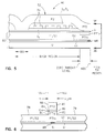
- Fig. 3 illustrates a portion of a merged MR head 46 showing the MR read head 50 and the write head 52.
- the merged MR head 46 is mounted on the slider 48.
- the read head 50 includes a magnetoresistive element MR which is sandwiched between first and second gap layers G1 and G2, the gap layers in turn being sandwiched between first and second shield layers S1 and S2.
- the second shield layer S2 of the read head 50 also serves as the bottom pole piece P1 for the write head 52 as will be explained in more detail hereinafter.
- the write head 52 has a pole tip region which is located between the air bearing surface (ABS) and a zero throat level and a yoke or back region which extends back from the zero throat level to and including a back gap.
- the write head 52 includes a bottom pole piece P1 and a top pole piece P2.
- the bottom pole piece P1 comprises the second shield layer S2 of the read head 50.
- Each pole piece P1 and P2 also has a back layer portion which is located in the back region, the back layer portions of the pole pieces being magnetically connected at the back gap (BG).
- the bottom pole piece P1 includes a pole tip structure which is located in the pole tip region between the ABS and the zero throat level.
- This pole tip structure includes a bottom pole tip element PT1a and a top pole tip element PT1b.
- the top pole piece P2 includes a pole tip structure which is located in the pole tip region between the ABS and the zero throat level.
- This pole tip structure includes a top pole tip element PT2.
- the pole tip elements PT1a and PT1b are integrally formed from second shield S2 of the read head 50 which will be explained in more detail hereinafter.
- a pole gap layer (G) is sandwiched between the pole tip elements PT1b and PT2.
- a desired thickness (gap length) of this layer is about 0.3 ⁇ m which will optimize the linear density of the write head without sacrificing its flux intensity. However, acceptable gap lengths range from 0.1 ⁇ m to 0.7 ⁇ m.
- the gap layer G may extend to the back gap BG or alternatively may terminate at the zero throat level.
- a first insulation layer I1 is deposited on top of the gap layer G by any suitable method such as photolithography.
- a coiled conductor layer 70 On top of the first insulation layer I1 there is deposited a coiled conductor layer 70 by any suitable method such as photoresist frame plating.
- second and third insulation layers I2 and I3 On top of the coiled conductor layer 70 there are deposited second and third insulation layers I2 and I3 by any suitable means, such as photolithography.
- the merged MR head 52 is referred to as "merged" because the bottom pole piece P1 and its pole tip comprise the second shield layer S2 of the MR read head, as shown in Figs. 5 and 6.
- One feature of a merged head is that a process step in depositing an extra magnetic layer is eliminated.
- the large width of the second shield layer S2 beyond the sides of the gap G, as illustrated in Fig. 6, causes flux to extend toward the second shield layer S2 beyond the width of the pole tip element PT2. This "side-fringing" flux causes sidewriting, which can degrade off-track performance.
- This problem has been overcome by notching the second shield layer S2 at 78 and 79 on each side of the gap G so as to provide the second shield layer S2 with a pedestal which forms a pole tip element PT1b.
- a pedestal which forms a pole tip element PT1b.
- Below the pedestal pole tip element PT1b is an area which can be referred to as a pole tip element PT1a.
- the pole tip elements PT1a and PT1b are forward extensions of the bottom pole piece P1 which comprises the second shield layer S2.
- the width of the second shield layer S2 is sufficient to effectively shield the MR element of the read head 50. This width can be in the order of 50 ⁇ m, in comparison to a width of 2 ⁇ m for the width of the pole tip elements.
- the notching 78 and 79 of the second shield layer S2 provides the pedestal pole tip element PT1b with first and second vertical sidewalls 80 and 82.
- the gap layer G has first and second vertical sidewalls 84 and 86.
- the pole tip element PT2 on top of the gap layer G has first and second vertical sidewalls 88 and 90.
- the vertical planes 100 and 102 are equally spaced from one another at the ABS to form the track width w of the write head 52.
- the first and second vertical planes 100 and 102 are also perpendicular to the ABS.
- the first and second vertical planes 100 and 102 are preferably equally spaced all the way from the ABS to the zero throat level. However, they could diverge from the ABS if desired.
- the vertical alignments of the sidewalls of the pole tip elements in the first and second vertical planes 100 and 102 are important in combination with the pedestal pole tip PT1b to minimize sidewriting caused by the large lateral width of the second shield layer S2. The importance of this pedestal pole tip PT1b is described in the next paragraph.
- Figs. 9 through 12 show the results of that analysis. The following apply to each of the Figs.
- the length of the pedestal pole tip element PT1b shown in Fig. 5 is three times the length of the gap, or 1.2 ⁇ m. It can be seen at 0.4 of the normalized head field that the sidetrack write field is very close to the minimum sidetrack write field of a pedestal pole tip element PT1b of infinite length. In Fig. 10, the length of the pedestal pole tip PT1b is two times the length of the gap, or 0.8 ⁇ m.
- the length of the pedestal pole tip PT1b is one times the length of the gap, or 0.4 ⁇ m, which has a performance which is still closer to the infinite pole tip represented by the "minimum” dashed line than it is to the absence of the pole tip represented by the "maximum” dashed line.
- Fig. 11 illustrates that even with a 0.4 ⁇ m notching of the second shield layer S2, a pedestal pole tip PT1b of a length 0.4 ⁇ m makes a considerable improvement in off-track performance of the write head over a write head which has no pedestal at all.
- Fig. 11 illustrates that even with a 0.4 ⁇ m notching of the second shield layer S2, a pedestal pole tip PT1b of a length 0.4 ⁇ m makes a considerable improvement in off-track performance of the write head over a write head which has no pedestal at all.
- the length of the pedestal pole tip PT1b is 0.5 times the length of the gap, or 0.2 ⁇ m. Even with a 0.2 ⁇ m length, the pedestal pole tip PT1b provides a 40% improvement over having no pedestal at all at the 0.4 normalized head field.
- the length of the pedestal pole tip PT1b can be very short and still accomplish significant improvement in off-track performance.
- An acceptable range for this length is 0.5 to 3.0 times the gap length with two times the gap length being the preferred or optimum length of the pedestal pole tip PT1b. It should be understood that the length of the gap may be different than the 0.4 ⁇ m demonstrated.
- the length of the gap can range all the way from 0.1 ⁇ m to 0.7 ⁇ m for acceptable performance.
- the notching or length of the pedestal pole tip PT1b would accordingly be 0.5 to 3.0 times the designed gap length.
- the pedestal element PT1b can be formed in the second shield layer S2 of the read head 50 without altering the performance of the layer S2 in shielding the MR element.
- the second shield layer S2 is typically 7 to 8 ⁇ m thick and a notching of approximately 1 ⁇ m will not affect its performance.
- the second shield layer S2 can be deposited with a greater thickness so as to allow for the notching 78 and 79. The important thing is that the notching saves a step in depositing a separate layer for the pedestal pole tip PT1b.
- a separate layer could be deposited on top of the second shield layer S2 and then appropriately notched to provide a pedestal pole tip element PT1b which is of a different material than the second shield layer S2.
- the pedestal pole tip PT1b can be constructed of a high moment of saturation material, such as ferric nitride, to handle a large amount of flux whereas the second shield layer S2 may be constructed of a lower moment of saturation material, such as Permalloy.
- the construction of the pedestal pole tip PT1b of a different material than the second shield layer S2 is discussed in more detail hereinafter.
- the pole tip element PT2 is formed on top of the second shield layer S2 with a gap G therebetween.
- the second shield layer S2 serves as the bottom pole piece P1 and, at its forward extension, the pole tip element PT1.
- the only element separating the pole tip element PT2 from the second shield layer S2 is the gap layer G. Because of the large lateral width of the S2 layer in comparison to the width of the pole tip element PT2, a substantial side-fringing field extends from the pole tip element PT2 beyond its width to the second shield layer S2.
- the flux would transit between the pole tip element PT2 and the second shield layer S2, acting as a pole tip element PT1, totally within the plane formed by the sidewalls of the pole tip element PT2. It is this desired performance that the merged MR head of Figs. 5 and 6 achieves.
- Fig. 13 illustrates an ABS view of a prior art inductive head.
- the inductive head includes pole tip elements PT1 and PT2 which are separated by a gap G.
- the inductive head employs the elements PT1, G and PT2 to perform both the read and write functions.
- a coil not shown, induces flux into the pole tip elements PT1 and PT2 to perform the write operation.
- the pole tip elements PT1 and PT2 and their corresponding pole pieces induce flux into the same coil for performing the read function.
- the off-track performance of this prior art inductive head is better than the off-track performance of the prior art merged MR head illustrated in Figs. 14 and 15.
- both pole tips PT2 and PT1 are milled by a downwardly directed ion beam during their construction.
- a substantial amount of redeposition of milled debris accumulates on the sidewalls of the milled pole tip elements causing the top pole tip element PT2 to shadow the bottom pole tip element PT1 thereby giving it its outwardly tapered shape, as shown in Fig. 13.
- the wider pole tip element PT1 in contrast to the pole tip element PT2 will cause some undesirable sidewriting.
- the ion milling of both pole tips (8 ⁇ m-10 ⁇ m) takes a long time.
- Figs. 7 and 8 illustrate another embodiment of the present invention which is slightly modified from the embodiment illustrated in Figs. 5 and 6.
- the top pole piece P2 is constructed of top and bottom magnetic layers 110 and 112 which have forward extensions forming pole tip elements PT2a and PT2b, respectively.
- the pole tip element PT2b has first and second vertical sidewalls 114 and 116 and the pole tip element PT2a has first and second vertical sidewalls 118 and 120.
- the pole tip element PT2a can be provided with a lateral width at the ABS which is considerably wider than the widths of the pole tip elements PT1b and PT2b.
- the pole tip elements PT2a and PT2b can be constructed in two separate layers when it is desired that the pole tip element PT2b be of a different material than the pole tip element PT2a.
- the pole element PT2b may be constructed of a high moment of saturation material, such as ferric nitride, whereas the pole tip element PT2a may be constructed of a lower moment of saturation material, such as Permalloy. With this arrangement, the pole tip element PT2b can carry a large amount of flux without saturation.
- the width of the pole tip elements for the present merged MR head 46 may be as narrow as 2 ⁇ m. This is less than the normal 4 to 5 ⁇ m for the width of the prior art inductive head illustrated in Fig. 13.
- the width of the pole tip elements PT1b and PT2 in Figs. 5 and 6 or the width of the pole tip elements PT1b and PT2b in Figs. 7 and 8 establishes the track width of the write head portion of the merged MR head. From this the TPI can be determined, which is a factor in producing the areal density of the write head.
- Figs. 3 and 4 illustrate a more complete embodiment of the write head with portions cut away to illustrate various details thereof. Part of a cover layer 112 has been broken away, the insulation layers I2 and I3 have been removed, and not all of the coiled conductor layer 70 is shown in Fig. 3.
- the conductor 70 extends around the back gap BG between the top and bottom pole pieces P2 and P1.
- One end of the coil conductor 70 is connected to a lead 72 at 73 and the other end of the conductor (not shown) is connected to a lead 74.
- the conductor 70 induces flux in the top and bottom pole pieces P2 and P1. This, in turn, induces flux back and forth across the pole tips at the ABS.
- the merged MR head of the present invention is constructed using a unique combination of known thin film photolithography and ion beam milling steps.
- Photolithography includes depositing magnetic layers using a photoresist frame plating process and depositing insulation layers by a photoresist and developing process.
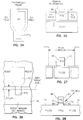
- Ion beam milling is performed in a chamber. Exemplary inner parts of such a chamber are illustrated in Fig. 16.
- the work piece (not shown) is placed on a turntable 130 and is rotated at a constant rpm. During rotation, one or more ion beams 132 and 134 are directed at the work piece.
- these ion beams are argon ions.
- the primary source ion beam 132 is shown directed vertically downward and the secondary source ion beam 134 is shown directed at an angle to a vertical.
- the ion beam milling of the preferred embodiment of the present invention is accomplished by beams which are directed only at some angle from a vertical.
- a shutter 136 is pivotally mounted for switching the ion beams on and off with respect to the work piece (not shown) on the turntable 130.
- the construction of the MR read head 50 portion of the merged MR head 46 is well known in the art.
- the layers S1, G1, the MR element, G2, and S2 are deposited by thin film photolithography process steps.
- the second shield layer S2 of the read head is deposited from the ABS to and including the back gap so that the S2 layer has a pole tip portion between the ABS and the zero throat level and a back portion between the zero throat level and the back gap.
- the bottom pole piece P1 of the write head 52 comprises this second shield layer S2. This combination defines a merged MR head.
- the pole tip structure of the top pole piece P2 is utilized as a mask for ion beam milling a pedestal into the pole tip structure of the bottom pole piece P1.
- the ion beam is directed at an angle to the sidewalls of the top pole tip structure either in a single angled beam or a pair of angled beams.
- the pair of angled beams is preferred and can be either directed sequentially or simultaneously.
- Instrumental in all embodiments is depositing the top pole tip structure with an additional thickness. This additional thickness will be reduced by the ion beam milling to form a pedestal in the bottom pole tip structure.
- Figs. 17 through 23 Various embodiments of directing the ion beam for constructing the Figs. 5 and 6 embodiment of the present invention are illustrated in Figs. 17 through 23.
- the pole tip element PT2 is employed as a mask for constructing the bottom pole tip structure. The same methods would be employed for constructing the Figs. 7 and 8 embodiment of the present invention.
- the pole tip element PT2b alone or the pole tip element PT2b and PT2a can be employed as a mask for forming the bottom pole tip structure.
- Figs. 17, 18, and 19 illustrate the use of two differently angled ion beams employed sequentially to form the bottom pole tip structure.
- Fig. 17 shows the pole tip element PT2 constructed with an extra thickness in order to allow for the reduction of thickness during the ion beam milling.
- the beginning thickness of the PT2 layer may be in the order of 7 ⁇ m with the extra thickness included in the order of 2 ⁇ m.
- the pole tip element PT2 is formed with vertical sides 88 and 90, the process for forming the pole tip element PT2 to be described in detail hereinafter.
- an ion beam is shown directed at an angle of 30° to the sidewall of the pole tip element PT2.
- the ion beam is shown directed at only the sidewall 90 of the pole tip element PT2, it will be directed at both sidewalls 88 and 90 of the pole tip element PT2 due to rotation of the work piece by the turntable 130, as described hereinabove.
- the gap layer G is deposited on top of the P1/S2 layer and the pole tip element PT2 is deposited on top of the gap layer G.
- a considerable amount of the material cut (debris) is redeposited (redep) on the sidewalls of the milled elements.
- the beam also performs a degree of clean up of the debris during the cutting operation.
- the 30° angle is a preferred angle, however, it can range between 20° to 40° for the two-angle embodiment.
- Fig. 17 shows the commencement of the cutting operation and
- Fig. 18 shows the final result of the cutting operation.
- the pole tip element PT2 acts as a mask for cutting the pedestal pole tip element PT1b in the second shield layer S2.
- the 30° ion beam is followed by a 75° ion beam, as illustrated in Fig. 19, to clean up the redep which is still left from the 30° operation.
- the 75° ion beam for clean up of the redep is preferred, however, this can range from 65° to 85° to the sidewalls of the pole tip element PT2. It should be noted that during the cutting operation the thickness of the pole tip element PT2 has been reduced by the additional thickness added (see Fig. 17), such as 2 ⁇ m. The surprising result is that after this milling, the sidewalls of the pedestal pole tip PT1b are aligned with the sidewalls of the pole tip element PT2. The pedestal pole tip PT1b has been formed by notching at 78 and 79 into the second shield layer S2.
- the gap layer G can either be ion milled by the 30° and 75° beams or alternatively can be chemically etched to its width prior to the ion beam milling.
- Figs. 20 and 21 show an embodiment of the ion beam milling which is similar to the Figs. 17, 18, and 19 embodiment except the 30° and 75° beams are directed simultaneously to perform the cutting and clean up operations.
- Figs. 22 and 23 illustrate an embodiment of the ion beam milling where a single ion beam is utilized for both cutting and clean up to define the pole tip pedestal PT1b.
- the previously described two-angle beam approach is preferred over the single beam. However, satisfactory results can be obtained with the single beam.
- the preferred angle for a single beam is 55°, however, it can vary from 45° to 65° as an acceptable range.
- Figs. 24 through 28 illustrate additional details in constructing the pole tip elements for the Figs. 5 and 6 embodiment of the present invention.
- a photoresist frame is utilized for plating the top pole piece P2 and its pole tip portion PT2. The plating operation also plates outside the frame, which is called the P2 field.
- the photoresist frame has been removed, leaving the pole tip PT2 with a P2 field on each side thereof.
- the gap layer G was deposited on top of the P1/S2 layer and the pole tip element PT2 was deposited on top of the gap layer G. With the frame plating process the pole tip element PT2 will be inherently constructed with vertically oriented sidewalls 88 and 90.
- Fig. 26 the P2 field has been removed and a photoresist mask has been placed on top of the P2 pole piece with an opening or window 140 exposing the pole tip element PT2.
- the resist window is illustrated more clearly in Fig. 27.
- One or more ion beams, as discussed hereinabove, are then directed through the resist window, as illustrated in Fig. 28, to notch the P1/S2 layer to provide the pedestal pole tip element PT1b.
- Figs. 29 through 33 illustrate process steps for making the pole tip structure of the Figs. 7 and 8 embodiment of the present invention. These steps are the same as that explained for Figs. 24 through 28 except the top pole piece P2 is constructed with two layers so as to provide two pole tip elements PT2a and PT2b, as illustrated in Fig. 30. After ion beam milling, as illustrated in Fig. 33, a pedestal pole tip element PT1b is formed and the top pole tip structure comprises pole tip elements PT2a and PT2b. As stated hereinabove, the pole tip element PT2b can be of a different material than the pole tip element PT2a.
- Fig. 29 through 33 illustrate process steps for making the pole tip structure of the Figs. 7 and 8 embodiment of the present invention. These steps are the same as that explained for Figs. 24 through 28 except the top pole piece P2 is constructed with two layers so as to provide two pole tip elements PT2a and PT2b, as illustrated in Fig. 30. After i
- the bottom pole tip structure would comprise two pedestal pole tip elements, namely pole tip element PT1b and PT1c.
- the pole tip element PT1c can be of a different material than the pole tip element PT1b.
- the pole tip elements PT2b and PT1c can be of a high moment of saturation material, (4 ⁇ m s ),such as ferric nitride, and the material for the pole tip elements PT1b and PT2a can be a lower moment of saturation material, such as Permalloy.
- the high saturation material will allow a large amount of flux to flow through the pole tips closest to the gap layer G without saturation.
- the method of making the merged MR head broadly includes the following steps: depositing the second shield layer S2 of the read head from the ABS to and including the back gap so that the S2 layer has a pole tip portion between the ABS and the zero throat level and a back portion between the zero throat level and the back gap (see Figs. 5 and 6); depositing the gap layer G on top of the second shield layer S2 from the ABS to the zero throat level (see Figs. 5 and 6); depositing a magnetic layer on top of the gap layer G and the second shield layer S2 to form the top pole piece P2 with a pole tip element PT2 on top of the gap layer G (see Figs.
- the step of directing at least one ion beam may comprise first and second ion beams, the first ion beam being at an angle ⁇ in the range of 0° ⁇ 60° and the second ion beam being at an angle ⁇ in the range of 60° ⁇ 85°.
- the step of depositing the gap layer G may include providing the gap layer with a thickness that defines a length g in the range of 0.1 ⁇ m to 0.7 ⁇ m with the length of the pole tip element P1lb at the ABS being in the range of 0.5g to 3.0g.
- the step of directing at least one ion beam may include notching the second shield layer S2 at 78 and 79 so that each notch is approximately 0.7 ⁇ m deep thereby providing the pole tip element PT1b with a length of approximately 0.7 ⁇ m; and the step of directing at least one ion beam including reducing the layer thickness of the pole tip element PT2 approximately 2 ⁇ m.
Landscapes
- Engineering & Computer Science (AREA)
- Manufacturing & Machinery (AREA)
- Magnetic Heads (AREA)
Applications Claiming Priority (2)
| Application Number | Priority Date | Filing Date | Title |
|---|---|---|---|
| US08/208,398 US5438747A (en) | 1994-03-09 | 1994-03-09 | Method of making a thin film merged MR head with aligned pole tips |
| US208398 | 2002-07-30 |
Publications (1)
| Publication Number | Publication Date |
|---|---|
| EP0671725A2 true EP0671725A2 (de) | 1995-09-13 |
Family
ID=22774467
Family Applications (1)
| Application Number | Title | Priority Date | Filing Date |
|---|---|---|---|
| EP95301460A Withdrawn EP0671725A2 (de) | 1994-03-09 | 1995-03-07 | Verschmolzener Dünnfilm-MR-Kopf |
Country Status (8)
| Country | Link |
|---|---|
| US (1) | US5438747A (de) |
| EP (1) | EP0671725A2 (de) |
| JP (1) | JP3045941B2 (de) |
| KR (1) | KR0150385B1 (de) |
| CN (1) | CN1058800C (de) |
| MY (1) | MY111561A (de) |
| SG (1) | SG28470A1 (de) |
| TW (1) | TW247363B (de) |
Cited By (3)
| Publication number | Priority date | Publication date | Assignee | Title |
|---|---|---|---|---|
| EP0835507A4 (de) * | 1995-06-05 | 1998-09-09 | Quantum Peripherals Colorado | Schreibwandler mit verbessertem fluss und herstellungsverfahren dafür mit gleichzeitiger herstellung von verteilten schutzblenden in einem magnetoresistiven lesekopf |
| CN1073253C (zh) * | 1996-04-26 | 2001-10-17 | 富士通株式会社 | 薄膜感应式磁头及磁读写驱动器 |
| SG94315A1 (en) * | 1997-05-27 | 2003-02-18 | Tdk Kabushiki Kaisha Tdk Corp | Thin film magnetic head |
Families Citing this family (154)
| Publication number | Priority date | Publication date | Assignee | Title |
|---|---|---|---|---|
| JPH07296331A (ja) * | 1993-08-27 | 1995-11-10 | Read Rite Corp | シールド付き書き込みポール構造を持つ磁気ヘッドアセンブリ |
| US5633771A (en) * | 1993-09-29 | 1997-05-27 | Kabushiki Kaisha Toshiba | Magnetoresistance effect type head and separate recording-reproducing type magnetic head |
| JP2854513B2 (ja) * | 1993-10-21 | 1999-02-03 | アルプス電気株式会社 | 複合型薄膜磁気ヘッド及びその製造方法 |
| US5739991A (en) * | 1994-02-01 | 1998-04-14 | Sanyo Electric Co., Ltd. | Composite thin film head having magnetoresistive and inductive head portions with nonmagnetic thin film interposed between core and shield portions of core layer |
| US5452164A (en) * | 1994-02-08 | 1995-09-19 | International Business Machines Corporation | Thin film magnetic write head |
| US5557491A (en) * | 1994-08-18 | 1996-09-17 | International Business Machines Corporation | Two terminal single stripe orthogonal MR head having biasing conductor integral with the lead layers |
| US5606478A (en) * | 1994-12-08 | 1997-02-25 | International Business Machines Corporation | Ni45 Fe55 metal-in-gap thin film magnetic head |
| US5578342A (en) * | 1995-07-05 | 1996-11-26 | Read-Rite Corporation | Alignment of magnetic poles of thin film transducer |
| WO1997008687A1 (en) * | 1995-08-23 | 1997-03-06 | Hitachi, Ltd. | Magnetic head and magnetic memory apparatus using the head |
| US5734531A (en) * | 1995-10-31 | 1998-03-31 | Quantum Peripherals Colorado, Inc. | Magneto-resistive read/write head having a combination pole/shield |
| US5784772A (en) * | 1995-12-21 | 1998-07-28 | Storage Technology Corporation | Method of simultaneously forming MR sensors in a dual element MR head |
| US6545847B2 (en) * | 1996-02-14 | 2003-04-08 | Hitachi, Ltd. | Magnetoresistive effect head |
| JP3349925B2 (ja) * | 1996-09-10 | 2002-11-25 | アルプス電気株式会社 | 薄膜磁気ヘッドの製造方法 |
| JP2953401B2 (ja) * | 1996-10-04 | 1999-09-27 | 日本電気株式会社 | 磁気抵抗効果型複合ヘッドの製造方法 |
| US5864450A (en) * | 1996-10-09 | 1999-01-26 | International Business Machines Corporation | NI45FE55 metal-in-gap thin film magnetic head |
| JP2980041B2 (ja) * | 1996-11-26 | 1999-11-22 | 日本電気株式会社 | 複合ヘッドの製造方法 |
| SG55435A1 (en) * | 1996-12-25 | 1998-12-21 | Hitachi Ltd | Thin film magnetic head and recording reproducing separate type magnetic head and magnetic recording reproducing apparatus using them |
| US5804085A (en) * | 1997-01-30 | 1998-09-08 | Quantum Corporation | Process for producing a pole-trimmed writer in a magnetoresistive read/write head and a data transducer made thereby |
| JPH10247305A (ja) * | 1997-03-03 | 1998-09-14 | Sanyo Electric Co Ltd | 複合型薄膜磁気ヘッドの製造方法 |
| JP2914343B2 (ja) * | 1997-04-07 | 1999-06-28 | 日本電気株式会社 | 磁気抵抗効果型複合ヘッド及びその製造方法並びに磁気記憶装置 |
| US5875542A (en) * | 1997-04-18 | 1999-03-02 | Read-Rite Corporation | Method of making thin film merged magnetoresistive heads |
| JPH117608A (ja) | 1997-04-25 | 1999-01-12 | Fujitsu Ltd | 磁気ヘッド及びその製造方法 |
| US5878481A (en) * | 1997-04-28 | 1999-03-09 | Headway Technologies, Inc. | Pole trimming method for fabricating a magnetic transducer structure |
| US5916423A (en) * | 1997-05-06 | 1999-06-29 | International Business Machines Corporation | P1 notched write head with minimum overmilled p1 and p2 |
| US5768070A (en) | 1997-05-14 | 1998-06-16 | International Business Machines Corporation | Horizontal thin film write, MR read head |
| JPH10334410A (ja) | 1997-05-29 | 1998-12-18 | Tdk Corp | 薄膜磁気ヘッド及びその製造方法 |
| US6178065B1 (en) | 1997-05-29 | 2001-01-23 | Tdk Corporation | Thin film magnetic head and manufacturing method of the head |
| US6201670B1 (en) * | 1997-06-16 | 2001-03-13 | International Business Machines Corporation | Merged magnetic head that includes a write head with single-sided notched first pole piece |
| JPH1131308A (ja) * | 1997-07-08 | 1999-02-02 | Nec Ibaraki Ltd | Mr複合ヘッドおよびその製造方法 |
| US6119331A (en) * | 1997-07-08 | 2000-09-19 | International Business Machines Corporation | Notching the first pole piece of a write head with a notching layer in a combined magnetic head |
| US6031695A (en) * | 1997-09-05 | 2000-02-29 | International Business Machines Corporation | Combined read head and write head with non-magnetic electrically conductive layer on upper pole tip thereof |
| JPH1186238A (ja) * | 1997-09-10 | 1999-03-30 | Fujitsu Ltd | 磁気ヘッド |
| JP3369444B2 (ja) * | 1997-09-12 | 2003-01-20 | ティーディーケイ株式会社 | 薄膜磁気ヘッド |
| US5905608A (en) * | 1997-09-19 | 1999-05-18 | International Business Machines Corporation | Dynamically tuned outer arms for improved rotary actuator performance |
| JP3795236B2 (ja) | 1997-10-01 | 2006-07-12 | Tdk株式会社 | 薄膜磁気ヘッド |
| US6018862A (en) * | 1997-10-07 | 2000-02-01 | Seagate Technology, Inc. | Thin-film magnetic recording head using a plated metal gap layer |
| US20040168302A1 (en) * | 1997-10-15 | 2004-09-02 | Tdk Corporation | Method for manufacturing thin-film magnetic head |
| US5940250A (en) * | 1997-10-21 | 1999-08-17 | Maxtor Corporation | Disk drive head having a read wide/write narrow architecture |
| JP3484332B2 (ja) | 1997-11-11 | 2004-01-06 | Tdk株式会社 | 薄膜磁気ヘッドの製造方法 |
| JP3790347B2 (ja) | 1997-11-26 | 2006-06-28 | Tdk株式会社 | 薄膜磁気ヘッドの製造方法 |
| US6105238A (en) * | 1997-12-04 | 2000-08-22 | Matsushita-Kotobukie Electronics Industries, Ltd. | Method and structure for defining track width on a recording head |
| US6024886A (en) * | 1997-12-05 | 2000-02-15 | Headway Technologies, Inc. | Planarizing method for fabricating an inductive magnetic write head for high density magnetic recording |
| JPH11232610A (ja) | 1997-12-12 | 1999-08-27 | Tdk Corp | 薄膜磁気ヘッド |
| US5867890A (en) * | 1997-12-17 | 1999-02-09 | International Business Machines Corporation | Method for making a thin film merged magnetoresistive read/inductive write head having a pedestal pole tip |
| US6069775A (en) * | 1997-12-22 | 2000-05-30 | International Business Machines Corporation | Inverted merged MR head with precise track width |
| US5901432A (en) * | 1997-12-24 | 1999-05-11 | International Business Machines Corporation | Method for making a thin film inductive write head having a pedestal pole tip and an electroplated gap |
| JPH11203627A (ja) * | 1998-01-12 | 1999-07-30 | Tdk Corp | 薄膜磁気ヘッド |
| US5996213A (en) * | 1998-01-30 | 1999-12-07 | Read-Rite Corporation | Thin film MR head and method of making wherein pole trim takes place at the wafer level |
| JP3782228B2 (ja) * | 1998-02-27 | 2006-06-07 | Tdk株式会社 | 複合型薄膜磁気ヘッドおよびその製造方法 |
| US6024884A (en) * | 1998-03-12 | 2000-02-15 | Storage Technology Corporation | Method for creating microstructures |
| JPH11288503A (ja) | 1998-04-02 | 1999-10-19 | Tdk Corp | 薄膜磁気ヘッドおよびその製造方法 |
| US6158107A (en) * | 1998-04-02 | 2000-12-12 | International Business Machines Corporation | Inverted merged MR head with plated notched first pole tip and self-aligned second pole tip |
| US6172848B1 (en) | 1998-04-10 | 2001-01-09 | International Business Machines Corporation | Write head with self aligned pedestal shaped pole tips that are separated by a zero throat height defining layer |
| US6317289B1 (en) | 1998-04-17 | 2001-11-13 | Tdk Corporation | Combination-type thin film magnetic head with improved writing properties |
| US6034848A (en) * | 1998-04-22 | 2000-03-07 | International Business Machines Corporation | Low profile multi-layer coil merged thin film magnetic head |
| US6055138A (en) * | 1998-05-06 | 2000-04-25 | Read-Rite Corporation | Thin film pedestal pole tips write head having narrower lower pedestal pole tip |
| JPH11328647A (ja) * | 1998-05-12 | 1999-11-30 | Hitachi Ltd | 磁気記録媒体および磁気記録媒体の製造方法 |
| JPH11339223A (ja) | 1998-05-26 | 1999-12-10 | Tdk Corp | 磁性層のエッチング方法、薄膜磁気ヘッドの磁極の形成方法および薄膜磁気ヘッドの製造方法 |
| JPH11353616A (ja) * | 1998-06-11 | 1999-12-24 | Tdk Corp | 薄膜磁気ヘッドおよびその製造方法 |
| US6510024B2 (en) | 1998-06-30 | 2003-01-21 | Fujitsu Limited | Magnetic head and method of manufacturing the same |
| JP3755560B2 (ja) | 1998-06-30 | 2006-03-15 | 富士通株式会社 | 磁気ヘッド及びその製造方法 |
| JP3428905B2 (ja) | 1998-06-30 | 2003-07-22 | ティーディーケイ株式会社 | 金属膜形成方法及び薄膜磁気ヘッドのポール形成方法 |
| JP2000020916A (ja) | 1998-07-01 | 2000-01-21 | Hitachi Ltd | 誘導型薄膜磁気ヘッド |
| JP2000105907A (ja) | 1998-07-30 | 2000-04-11 | Tdk Corp | 薄膜磁気ヘッドおよびその製造方法 |
| JP3469473B2 (ja) | 1998-08-26 | 2003-11-25 | Tdk株式会社 | 薄膜磁気ヘッドおよびその製造方法 |
| US6317288B1 (en) | 1998-08-28 | 2001-11-13 | Tdk Corporation | Thin-film magnetic head and method of manufacturing same |
| JP3306011B2 (ja) | 1998-09-22 | 2002-07-24 | 日本電気株式会社 | 磁気抵抗効果型複合ヘッドおよびその製造方法 |
| JP3503874B2 (ja) | 1998-09-29 | 2004-03-08 | Tdk株式会社 | 薄膜磁気ヘッドの製造方法 |
| JP2000113412A (ja) | 1998-10-07 | 2000-04-21 | Tdk Corp | 薄膜磁気ヘッドおよびその製造方法 |
| JP2000149219A (ja) | 1998-11-12 | 2000-05-30 | Tdk Corp | 薄膜磁気ヘッドおよびその製造方法 |
| JP3180906B2 (ja) * | 1998-11-12 | 2001-07-03 | 日本電気株式会社 | 磁気抵抗効果型複合ヘッドの製造方法 |
| JP3523092B2 (ja) | 1998-11-18 | 2004-04-26 | Tdk株式会社 | 薄膜磁気ヘッドおよびその製造方法 |
| JP3781399B2 (ja) | 1998-12-08 | 2006-05-31 | Tdk株式会社 | 薄膜磁気ヘッドおよびその製造方法 |
| US6176005B1 (en) | 1998-12-15 | 2001-01-23 | International Business Machines Corporation | Method of making read head with improved lead layers |
| US6765756B1 (en) | 1999-03-12 | 2004-07-20 | Western Digital (Fremont), Inc. | Ultra-short yoke and ultra-low stack height writer and method of fabrication |
| US6464891B1 (en) | 1999-03-17 | 2002-10-15 | Veeco Instruments, Inc. | Method for repetitive ion beam processing with a carbon containing ion beam |
| JP3373167B2 (ja) | 1999-03-24 | 2003-02-04 | ティーディーケイ株式会社 | 薄膜磁気ヘッドの製造方法 |
| JP3530064B2 (ja) | 1999-03-29 | 2004-05-24 | Tdk株式会社 | 薄膜磁気ヘッドおよびその製造方法ならびに薄膜磁気ヘッド用素材およびその製造方法 |
| US6238582B1 (en) | 1999-03-30 | 2001-05-29 | Veeco Instruments, Inc. | Reactive ion beam etching method and a thin film head fabricated using the method |
| JP3856587B2 (ja) | 1999-04-06 | 2006-12-13 | Tdk株式会社 | 薄膜磁気ヘッドおよびその製造方法 |
| US6282056B1 (en) | 1999-04-08 | 2001-08-28 | Read-Rite Corporation | Tapered stitch pole writer for high density magnetic recording |
| US6657816B1 (en) * | 1999-04-09 | 2003-12-02 | Ronald A. Barr | Thin film inductive read/write head with a sloped pole |
| JP3856591B2 (ja) | 1999-04-28 | 2006-12-13 | Tdk株式会社 | 薄膜磁気ヘッドおよびその製造方法 |
| US6224719B1 (en) * | 1999-05-13 | 2001-05-01 | International Business Machines Corporation | Sputtering method of manufacturing Fe-Ai-N-O laminated films using N2O as the reactive gas |
| JP3421635B2 (ja) | 1999-06-04 | 2003-06-30 | ティーディーケイ株式会社 | 薄膜磁気ヘッドおよびその製造方法 |
| US6342990B1 (en) | 1999-06-14 | 2002-01-29 | Tdk Corporation | Method for forming magnetic pole layer of thin film magnetic head, thin film magnetic head and method for manufacturing the same |
| JP3522593B2 (ja) | 1999-06-15 | 2004-04-26 | Tdk株式会社 | 薄膜磁気ヘッドおよびその製造方法 |
| JP3527138B2 (ja) | 1999-06-17 | 2004-05-17 | Tdk株式会社 | 薄膜磁気ヘッドおよびその製造方法ならびに薄膜コイル素子およびその製造方法 |
| JP3526787B2 (ja) | 1999-06-25 | 2004-05-17 | Tdk株式会社 | 薄膜磁気ヘッドおよびその製造方法 |
| JP3859398B2 (ja) | 1999-07-08 | 2006-12-20 | Tdk株式会社 | 薄膜磁気ヘッドおよびその製造方法 |
| US7012784B2 (en) * | 1999-07-08 | 2006-03-14 | Tdk Corporation | Thin-film magnetic head and method of manufacturing same |
| JP3373176B2 (ja) * | 1999-07-09 | 2003-02-04 | ティーディーケイ株式会社 | 薄膜磁気ヘッドの製造方法および薄膜磁気ヘッド |
| JP3522595B2 (ja) | 1999-07-14 | 2004-04-26 | Tdk株式会社 | 薄膜磁気ヘッドおよびその製造方法 |
| JP3490643B2 (ja) | 1999-07-14 | 2004-01-26 | Tdk株式会社 | 薄膜磁気ヘッドの製造方法 |
| JP2001034911A (ja) | 1999-07-16 | 2001-02-09 | Tdk Corp | 薄膜磁気ヘッドおよびその製造方法 |
| JP2001043510A (ja) * | 1999-07-30 | 2001-02-16 | Fujitsu Ltd | 磁気ヘッド及びその製造方法 |
| JP3473684B2 (ja) | 1999-11-08 | 2003-12-08 | 日本電気株式会社 | 磁気ヘッドおよびその製造方法、それを用いる磁気記録再生装置 |
| JP2001067617A (ja) | 1999-08-24 | 2001-03-16 | Tdk Corp | 薄膜磁気ヘッドおよびその製造方法 |
| US6317290B1 (en) | 1999-08-31 | 2001-11-13 | Read-Rite Corporation | Advance pole trim writer with moment P1 and low apex angle |
| US6452742B1 (en) | 1999-09-02 | 2002-09-17 | Read-Rite Corporation | Thin film write having reduced resistance conductor coil partially recessed within middle coat insulation |
| JP3530084B2 (ja) | 1999-09-07 | 2004-05-24 | Tdk株式会社 | 薄膜磁気ヘッドおよびその製造方法 |
| JP2001084514A (ja) | 1999-09-16 | 2001-03-30 | Tdk Corp | 薄膜磁気ヘッドおよびその製造方法 |
| US6791794B2 (en) | 2000-09-28 | 2004-09-14 | Nec Corporation | Magnetic head having an antistripping layer for preventing a magnetic layer from stripping |
| US6243939B1 (en) | 1999-10-04 | 2001-06-12 | Headway Technologies, Inc. | High ion beam etch selectivity for partial pole trim application |
| JP3492953B2 (ja) * | 1999-10-05 | 2004-02-03 | Tdk株式会社 | 薄膜磁気ヘッドの製造方法 |
| JP2001110008A (ja) | 1999-10-06 | 2001-04-20 | Nec Corp | 磁気ヘッドおよびその製造方法、および磁気記録再生装置 |
| JP3869595B2 (ja) | 1999-11-12 | 2007-01-17 | Tdk株式会社 | 薄膜磁気ヘッドおよびその製造方法 |
| US6460243B1 (en) * | 1999-11-22 | 2002-10-08 | International Business Machines Corporation | Method of making low stress and low resistance rhodium (RH) leads |
| JP3440224B2 (ja) | 1999-11-29 | 2003-08-25 | Tdk株式会社 | 薄膜磁気ヘッドおよびその製造方法 |
| US7002776B2 (en) | 1999-12-06 | 2006-02-21 | Tdk Corporation | Thin film magnetic head and method of manufacturing same |
| JP2001167406A (ja) | 1999-12-07 | 2001-06-22 | Tdk Corp | 薄膜磁気ヘッドおよびその製造方法 |
| JP3440225B2 (ja) | 1999-12-09 | 2003-08-25 | Tdk株式会社 | フレームめっき方法および薄膜磁気ヘッドの磁極の形成方法 |
| JP2001167408A (ja) | 1999-12-09 | 2001-06-22 | Tdk Corp | 薄膜磁気ヘッドおよびその製造方法 |
| JP2001195706A (ja) | 2000-01-05 | 2001-07-19 | Nec Corp | 記録ヘッド、記録ヘッドの製造方法、及び複合ヘッド並びに磁気記録再生装置 |
| US6594112B1 (en) * | 2000-01-05 | 2003-07-15 | Seagate Technology Llc | Magnetic recording head with a precision throatheight-defining structure |
| JP3565492B2 (ja) | 2000-02-17 | 2004-09-15 | Tdk株式会社 | 薄膜磁気ヘッド、磁気ヘッド装置及び磁気ディスク装置 |
| US6687096B2 (en) | 2000-06-21 | 2004-02-03 | Tdk Corporation | Thin-film magnetic head and method of manufacturing same |
| JP2002015405A (ja) * | 2000-06-28 | 2002-01-18 | Tdk Corp | 薄膜磁気ヘッドおよびその製造方法 |
| JP2002015404A (ja) | 2000-06-29 | 2002-01-18 | Tdk Corp | 薄膜磁気ヘッドおよびその製造方法 |
| US6539610B1 (en) * | 2000-07-14 | 2003-04-01 | International Business Machines Corporation | Method for manufacturing a magnetic write head |
| JP2002063703A (ja) | 2000-08-18 | 2002-02-28 | Tdk Corp | 薄膜パターン形成方法および薄膜磁気ヘッドの磁極の形成方法 |
| JP3617953B2 (ja) | 2000-09-18 | 2005-02-09 | Tdk株式会社 | 薄膜磁気ヘッドの製造方法 |
| JP2002170208A (ja) * | 2000-11-22 | 2002-06-14 | Shinka Jitsugyo Kk | 薄膜磁気ヘッドおよびその製造方法 |
| JP3593312B2 (ja) | 2000-12-26 | 2004-11-24 | アルプス電気株式会社 | 垂直磁気記録ヘッドおよびその製造方法 |
| US6765757B2 (en) * | 2001-01-15 | 2004-07-20 | Alps Electric Co., Ltd. | Soft magnetic film having high saturation magnetic flux density, thin-film magnetic head using the same, and manufacturing method of the same |
| JP4176322B2 (ja) * | 2001-03-26 | 2008-11-05 | Tdk株式会社 | 薄膜形成方法、及び薄膜磁気ヘッドの製造方法 |
| US6654203B2 (en) | 2001-04-25 | 2003-11-25 | Tdk Corporation | Thin-film magnetic head and method of manufacturing same, head gimbal assembly and hard disk drive |
| US6678117B2 (en) | 2001-06-18 | 2004-01-13 | Hitachi Global Storage Technologies Netherlands B.V. | Magnetic transducer with bilayer pole piece structure with improved milling endpoint detection |
| US6656371B2 (en) * | 2001-09-27 | 2003-12-02 | Micron Technology, Inc. | Methods of forming magnetoresisitive devices |
| US6656372B2 (en) * | 2001-10-04 | 2003-12-02 | Micron Technology, Inc. | Methods of making magnetoresistive memory devices |
| US6947255B2 (en) * | 2002-03-22 | 2005-09-20 | International Business Machines Corporation | Magnetic head having a notched pole piece structure and method of making the same |
| JP2004127404A (ja) * | 2002-10-01 | 2004-04-22 | Tdk Corp | 薄膜磁気ヘッド、磁気ヘッド装置及び磁気記録再生装置 |
| JP3865308B2 (ja) * | 2002-10-02 | 2007-01-10 | Tdk株式会社 | 薄膜磁気ヘッド、磁気ヘッド装置及び磁気記録再生装置 |
| US6887355B2 (en) * | 2002-10-31 | 2005-05-03 | Headway Technologies, Inc. | Self-aligned pole trim process |
| US20050034298A1 (en) * | 2003-08-15 | 2005-02-17 | Hitachi Global Storage Technologies | Disk drive yield optimization by capacity |
| US7133255B2 (en) * | 2003-08-27 | 2006-11-07 | Hitachi Global Storage Technologies Netherlands, B.V. | Magnetic head having magnetic pole with lengthened neck pole tip and coplanar yoke, and method of fabrication thereof |
| JP2005293762A (ja) * | 2004-04-02 | 2005-10-20 | Tdk Corp | 複合型薄膜磁気ヘッド |
| US7086139B2 (en) * | 2004-04-30 | 2006-08-08 | Hitachi Global Storage Technologies Netherlands B.V. | Methods of making magnetic write heads using electron beam lithography |
| US7480983B2 (en) * | 2004-05-28 | 2009-01-27 | Hitachi Global Storage Technologies Netherlands B.V. | Method for making magnetic write head |
| US8815060B2 (en) * | 2004-08-30 | 2014-08-26 | HGST Netherlands B.V. | Method for minimizing magnetically dead interfacial layer during COC process |
| US7363698B2 (en) * | 2004-09-30 | 2008-04-29 | Hitachi Gobal Storage Technologies Inc. | Process for creating a write head by forming a bump after the top pole is formed |
| JP2007184022A (ja) | 2006-01-04 | 2007-07-19 | Alps Electric Co Ltd | 垂直磁気記録ヘッドの主磁極形成方法 |
| US7969684B2 (en) * | 2006-03-28 | 2011-06-28 | Hitachi Global Storage Technologies Netherlands B.V. | Write head design and method for reducing adjacent track interference at very narrow track widths |
| US7536774B2 (en) * | 2006-04-07 | 2009-05-26 | Hitachi Global Storage Technologies B.V. | Method and apparatus for integrating a stair notch and a gap bump at a pole tip in a write head |
| US7768741B2 (en) * | 2006-05-22 | 2010-08-03 | Hitachi Global Storage Technologies Netherlands B.V. | Magnetic write head design for reducing wide area track erasure |
| US7716813B2 (en) * | 2006-12-05 | 2010-05-18 | Hitachi Global Storage Technologies Netherlands B.V. | Method for fabricating magnetic write pole for a magnetic head using an E-beam resist mask |
| US8361284B2 (en) * | 2007-05-03 | 2013-01-29 | Hgst, Netherlands B.V. | Reducing the height of a defect associated with an air bearing surface |
| US20090273859A1 (en) * | 2008-05-02 | 2009-11-05 | Flint Eric W | Forming a pole tip topography |
| US8080167B2 (en) | 2009-02-20 | 2011-12-20 | Tdk Corporation | Shaping method of thin film and manufacturing method of perpendicular recording magnetic head using the same |
| US8790524B1 (en) | 2010-09-13 | 2014-07-29 | Western Digital (Fremont), Llc | Method and system for providing a magnetic recording transducer using a line hard mask and a wet-etchable mask |
| CA2791249C (en) * | 2011-11-10 | 2014-02-25 | Semiconductor Insights Inc. | Method and system for ion beam delayering of a sample and control thereof |
| US8607438B1 (en) | 2011-12-01 | 2013-12-17 | Western Digital (Fremont), Llc | Method for fabricating a read sensor for a read transducer |
| US9406331B1 (en) | 2013-06-17 | 2016-08-02 | Western Digital (Fremont), Llc | Method for making ultra-narrow read sensor and read transducer device resulting therefrom |
| US9007719B1 (en) | 2013-10-23 | 2015-04-14 | Western Digital (Fremont), Llc | Systems and methods for using double mask techniques to achieve very small features |
Family Cites Families (9)
| Publication number | Priority date | Publication date | Assignee | Title |
|---|---|---|---|---|
| JPS6035315A (ja) * | 1983-08-04 | 1985-02-23 | Nec Corp | 薄膜磁気ヘッド |
| JPS61130848A (ja) * | 1984-11-30 | 1986-06-18 | Hitachi Naka Seiki Kk | 電子線終点検知機構付イオンミリング装置 |
| US4918554A (en) * | 1988-09-27 | 1990-04-17 | International Business Machines Corporation | Process for making a shielded magnetoresistive sensor |
| JP2728487B2 (ja) * | 1989-02-08 | 1998-03-18 | 株式会社日立製作所 | 録再分離複合型磁気ヘッド |
| JP2754804B2 (ja) * | 1989-11-20 | 1998-05-20 | 松下電器産業株式会社 | 薄膜磁気ヘッドの製造方法 |
| US5116719A (en) * | 1990-02-15 | 1992-05-26 | Seagate Technology, Inc. | Top pole profile for pole tip trimming |
| US5200056A (en) * | 1990-02-15 | 1993-04-06 | Seagate Technology Inc. | Method for aligning pole tips in a thin film head |
| JP2830559B2 (ja) * | 1991-11-20 | 1998-12-02 | 日本電気株式会社 | 複合型薄膜磁気ヘッドの製造方法 |
| JPH07220245A (ja) * | 1994-02-01 | 1995-08-18 | Sanyo Electric Co Ltd | 複合型磁気ヘッド |
-
1994
- 1994-03-09 US US08/208,398 patent/US5438747A/en not_active Expired - Lifetime
- 1994-09-20 MY MYPI94002500A patent/MY111561A/en unknown
- 1994-10-14 TW TW083109551A patent/TW247363B/zh active
- 1994-12-09 CN CN94112929A patent/CN1058800C/zh not_active Expired - Fee Related
- 1994-12-27 JP JP6325467A patent/JP3045941B2/ja not_active Expired - Fee Related
-
1995
- 1995-02-28 KR KR1019950004119A patent/KR0150385B1/ko not_active Expired - Fee Related
- 1995-03-07 EP EP95301460A patent/EP0671725A2/de not_active Withdrawn
- 1995-03-08 SG SG1995000073A patent/SG28470A1/en unknown
Cited By (3)
| Publication number | Priority date | Publication date | Assignee | Title |
|---|---|---|---|---|
| EP0835507A4 (de) * | 1995-06-05 | 1998-09-09 | Quantum Peripherals Colorado | Schreibwandler mit verbessertem fluss und herstellungsverfahren dafür mit gleichzeitiger herstellung von verteilten schutzblenden in einem magnetoresistiven lesekopf |
| CN1073253C (zh) * | 1996-04-26 | 2001-10-17 | 富士通株式会社 | 薄膜感应式磁头及磁读写驱动器 |
| SG94315A1 (en) * | 1997-05-27 | 2003-02-18 | Tdk Kabushiki Kaisha Tdk Corp | Thin film magnetic head |
Also Published As
| Publication number | Publication date |
|---|---|
| JPH07262519A (ja) | 1995-10-13 |
| JP3045941B2 (ja) | 2000-05-29 |
| CN1058800C (zh) | 2000-11-22 |
| KR0150385B1 (ko) | 1998-10-15 |
| US5438747A (en) | 1995-08-08 |
| TW247363B (en) | 1995-05-11 |
| CN1122496A (zh) | 1996-05-15 |
| KR950027691A (ko) | 1995-10-18 |
| SG28470A1 (en) | 1996-04-01 |
| MY111561A (en) | 2000-08-30 |
Similar Documents
| Publication | Publication Date | Title |
|---|---|---|
| US5438747A (en) | Method of making a thin film merged MR head with aligned pole tips | |
| US5452164A (en) | Thin film magnetic write head | |
| US6104576A (en) | Inductive head with reduced height insulation stack due to partial coverage zero throat height defining insulation layer | |
| US6195229B1 (en) | Thin film MR head and method of making wherein pole trim takes place at the wafer level | |
| KR100273618B1 (ko) | 자기 헤드 어셈블리, 자기 디스크 드라이브 및 자기 헤드 어셈블리 제조 방법 | |
| US5867890A (en) | Method for making a thin film merged magnetoresistive read/inductive write head having a pedestal pole tip | |
| US5349745A (en) | Method of fabricating thin-film magnetic head | |
| US6278591B1 (en) | Inverted merged MR head having plated notched first pole tip and self-aligned second pole tip | |
| JPH05334621A (ja) | 磁気記録ヘッド及びその製造方法 | |
| US6785953B2 (en) | Process of fabricating a write head with protection of a second pole tip thickness | |
| US6081408A (en) | Magnetoresistive read/write head having reduced write fringing and method for manufacturing same | |
| JP2005317188A (ja) | 平面型垂直記録用ヘッド | |
| US5867889A (en) | Double self-aligned insulated contiguous junction for flux-guided-MR or yoke-MR head applications | |
| US6665156B2 (en) | Magnetoresistive head, manufacture thereof, and magnetic recording/reproducing apparatus with such magnetic head | |
| JP2725618B2 (ja) | 薄膜磁気ヘッドおよびその製造方法 | |
| US6328859B1 (en) | Method of making second pole tip of a write head with a narrow track width | |
| US6477765B1 (en) | Method of fabricating a magnetic write transducer | |
| US5894389A (en) | Thin-film Magnetic head having a narrow core width and process for its production | |
| US20100321824A1 (en) | Magnetic recording head having secondary sub-gaps | |
| KR20020007157A (ko) | 폭이 좁은 기록 트랙폭을 갖는 박막 유도성 판독 기록헤드와, 그 제조 방법 및 사용 방법 | |
| JP3639529B2 (ja) | 薄膜磁気ヘッド及び薄膜磁気ヘッドの製造方法 | |
| US5778514A (en) | Method for forming a transducing head | |
| US7092207B2 (en) | Thin film magnetic head and method of manufacturing the same | |
| JPH08185613A (ja) | 磁気抵抗型薄膜磁気ヘッドおよびその製造方法 | |
| US6873498B2 (en) | Magnetic head and method of manufacturing the same |
Legal Events
| Date | Code | Title | Description |
|---|---|---|---|
| PUAI | Public reference made under article 153(3) epc to a published international application that has entered the european phase |
Free format text: ORIGINAL CODE: 0009012 |
|
| AK | Designated contracting states |
Kind code of ref document: A2 Designated state(s): DE FR GB |
|
| 17P | Request for examination filed |
Effective date: 19960119 |
|
| STAA | Information on the status of an ep patent application or granted ep patent |
Free format text: STATUS: THE APPLICATION HAS BEEN WITHDRAWN |
|
| 18W | Application withdrawn |
Withdrawal date: 19960409 |