EP0671742A1 - Signalisation du type de défauts d'un support d'information optique - Google Patents
Signalisation du type de défauts d'un support d'information optique Download PDFInfo
- Publication number
- EP0671742A1 EP0671742A1 EP95103711A EP95103711A EP0671742A1 EP 0671742 A1 EP0671742 A1 EP 0671742A1 EP 95103711 A EP95103711 A EP 95103711A EP 95103711 A EP95103711 A EP 95103711A EP 0671742 A1 EP0671742 A1 EP 0671742A1
- Authority
- EP
- European Patent Office
- Prior art keywords
- error
- cause
- signal
- frequency signal
- fingerprint
- Prior art date
- Legal status (The legal status is an assumption and is not a legal conclusion. Google has not performed a legal analysis and makes no representation as to the accuracy of the status listed.)
- Granted
Links
- 230000003287 optical effect Effects 0.000 title claims description 49
- 230000007547 defect Effects 0.000 title abstract description 4
- 238000005259 measurement Methods 0.000 claims description 39
- 238000000034 method Methods 0.000 claims description 34
- 238000012545 processing Methods 0.000 claims description 24
- 230000011664 signaling Effects 0.000 claims description 16
- 239000000969 carrier Substances 0.000 claims description 13
- 230000002950 deficient Effects 0.000 claims description 8
- 239000003990 capacitor Substances 0.000 claims description 7
- 241000486634 Bena Species 0.000 claims 1
- PCHPORCSPXIHLZ-UHFFFAOYSA-N diphenhydramine hydrochloride Chemical compound [Cl-].C=1C=CC=CC=1C(OCC[NH+](C)C)C1=CC=CC=C1 PCHPORCSPXIHLZ-UHFFFAOYSA-N 0.000 claims 1
- 238000011156 evaluation Methods 0.000 abstract description 4
- 238000010586 diagram Methods 0.000 description 6
- 238000012937 correction Methods 0.000 description 4
- 238000004519 manufacturing process Methods 0.000 description 2
- 238000012360 testing method Methods 0.000 description 2
- 238000004364 calculation method Methods 0.000 description 1
- 238000013016 damping Methods 0.000 description 1
- 230000006735 deficit Effects 0.000 description 1
- 238000013461 design Methods 0.000 description 1
- 238000005516 engineering process Methods 0.000 description 1
- 230000007613 environmental effect Effects 0.000 description 1
- 235000015244 frankfurter Nutrition 0.000 description 1
- 238000007689 inspection Methods 0.000 description 1
- 230000010354 integration Effects 0.000 description 1
- 239000010410 layer Substances 0.000 description 1
- 230000035515 penetration Effects 0.000 description 1
- 239000011241 protective layer Substances 0.000 description 1
- 238000003908 quality control method Methods 0.000 description 1
- 230000005236 sound signal Effects 0.000 description 1
- 230000001360 synchronised effect Effects 0.000 description 1
- 230000000007 visual effect Effects 0.000 description 1
Images



Classifications
-
- G—PHYSICS
- G11—INFORMATION STORAGE
- G11B—INFORMATION STORAGE BASED ON RELATIVE MOVEMENT BETWEEN RECORD CARRIER AND TRANSDUCER
- G11B7/00—Recording or reproducing by optical means, e.g. recording using a thermal beam of optical radiation by modifying optical properties or the physical structure, reproducing using an optical beam at lower power by sensing optical properties; Record carriers therefor
- G11B7/08—Disposition or mounting of heads or light sources relatively to record carriers
- G11B7/09—Disposition or mounting of heads or light sources relatively to record carriers with provision for moving the light beam or focus plane for the purpose of maintaining alignment of the light beam relative to the record carrier during transducing operation, e.g. to compensate for surface irregularities of the latter or for track following
- G11B7/0948—Disposition or mounting of heads or light sources relatively to record carriers with provision for moving the light beam or focus plane for the purpose of maintaining alignment of the light beam relative to the record carrier during transducing operation, e.g. to compensate for surface irregularities of the latter or for track following specially adapted for detection and avoidance or compensation of imperfections on the carrier, e.g. dust, scratches, dropouts
-
- G—PHYSICS
- G11—INFORMATION STORAGE
- G11B—INFORMATION STORAGE BASED ON RELATIVE MOVEMENT BETWEEN RECORD CARRIER AND TRANSDUCER
- G11B27/00—Editing; Indexing; Addressing; Timing or synchronising; Monitoring; Measuring tape travel
- G11B27/36—Monitoring, i.e. supervising the progress of recording or reproducing
-
- G—PHYSICS
- G11—INFORMATION STORAGE
- G11B—INFORMATION STORAGE BASED ON RELATIVE MOVEMENT BETWEEN RECORD CARRIER AND TRANSDUCER
- G11B20/00—Signal processing not specific to the method of recording or reproducing; Circuits therefor
- G11B20/10—Digital recording or reproducing
- G11B20/18—Error detection or correction; Testing, e.g. of drop-outs
- G11B20/1816—Testing
-
- G—PHYSICS
- G11—INFORMATION STORAGE
- G11B—INFORMATION STORAGE BASED ON RELATIVE MOVEMENT BETWEEN RECORD CARRIER AND TRANSDUCER
- G11B27/00—Editing; Indexing; Addressing; Timing or synchronising; Monitoring; Measuring tape travel
- G11B27/10—Indexing; Addressing; Timing or synchronising; Measuring tape travel
- G11B27/34—Indicating arrangements
-
- G—PHYSICS
- G11—INFORMATION STORAGE
- G11B—INFORMATION STORAGE BASED ON RELATIVE MOVEMENT BETWEEN RECORD CARRIER AND TRANSDUCER
- G11B33/00—Constructional parts, details or accessories not provided for in the other groups of this subclass
- G11B33/10—Indicating arrangements; Warning arrangements
-
- G—PHYSICS
- G11—INFORMATION STORAGE
- G11B—INFORMATION STORAGE BASED ON RELATIVE MOVEMENT BETWEEN RECORD CARRIER AND TRANSDUCER
- G11B2220/00—Record carriers by type
- G11B2220/20—Disc-shaped record carriers
-
- G—PHYSICS
- G11—INFORMATION STORAGE
- G11B—INFORMATION STORAGE BASED ON RELATIVE MOVEMENT BETWEEN RECORD CARRIER AND TRANSDUCER
- G11B2220/00—Record carriers by type
- G11B2220/20—Disc-shaped record carriers
- G11B2220/25—Disc-shaped record carriers characterised in that the disc is based on a specific recording technology
- G11B2220/2537—Optical discs
- G11B2220/2545—CDs
-
- G—PHYSICS
- G11—INFORMATION STORAGE
- G11B—INFORMATION STORAGE BASED ON RELATIVE MOVEMENT BETWEEN RECORD CARRIER AND TRANSDUCER
- G11B2220/00—Record carriers by type
- G11B2220/20—Disc-shaped record carriers
- G11B2220/25—Disc-shaped record carriers characterised in that the disc is based on a specific recording technology
- G11B2220/2537—Optical discs
- G11B2220/2587—Laser Discs; Optical disc using analog recording
Definitions
- the invention relates to a method and an arrangement for error type signaling of optical information carriers with a playback device in the sense of a Fuzzy Logic ", which signals not only the presence of an error, but the type of error, such as fingerprints on a compact disc, thereby enabling the consumer, if necessary, to restore the original reproduction quality of the optical information carrier.
- optical information carriers used for recording and reproducing audio and / or video signals or data signals have both manufacturing and environmental errors, which are to a certain extent corrected or interpolated by the playback devices using an error correction device.
- the Compact Disc or Laserdisc would not be possible without this capability, since none of the many bits would then be lost or none of the countless pits in the disk should be smeared or covered.
- errors in the optical information carrier can at least influence the originality of the reproduction or lead to failures in the reproduction.
- an error display device which shows the utilization of the error correction, cf. KRIEG, Bernhard: Practice of digital audio technology: digital recording and playback, Franzis-Verlag GmbH, Kunststoff 1989, pp. 60 - 63.
- the utilization of the error correction is a reflection of the degree of error of the optical information carrier, which is signaled by the program counter in the player .
- the degree of error represents both the frequency and the number of errors.
- a method for determining errors in signals stored on disc-shaped, rotating information carriers in spiral tracks in which an error signal is identified by comparison with the signal content of previous revolutions in such a way that when the error signal is repeated in the next revolution, a scratch and without repetition an individual error is registered, cf. DE-OS 28 51 822.
- a shift register with the length of one revolution is provided for carrying out the method. Spatially limited errors are found electronically in some specific way and are given as a pulse signal to the input of the device.
- the method is based on comparing an error signal with the signal content of previous revolutions. A repetition of the error signal in the radial direction at the same location in the next revolution is registered with a shift register.
- the invention is therefore based on the task of creating a method and an arrangement with little effort the signaling of at least one type of error in an optical recording medium, such as fingerprints, is made possible with a playback device, so that the advice or signaling system makes it easier for the consumer to assess the quality of the optical recording medium and provides information on achieving better playback quality when the cause of the error is fingerprint becomes.
- the object is achieved according to the invention in that at least one cause or type of error is determined in a first method step and signaled or displayed in a second method step.
- the optical information carrier being played back has an error
- at least one cause of error is explicitly displayed, so that in the event of the cause of the error fingerprint by simply wiping the fingerprints, preferably in a straight line from the center to the edge, the consumer can restore the original reproduction quality.
- the starting point of the method is the optical information carrier, which, in particular due to multiple and negligent handling, increasingly has errors and is optically scanned with a playback device that is normally used to reproduce the information.
- a number of defective frames representing the degree of error of an optical disk which is no longer corrected by the decoder, is related to the location of the error in order to determine the cause of the error from the degree of error, the error location being the number of Subcode blocks between error packets evaluated according to the error rate can be determined. This will cause the error determined with an error rate occurring in adjacent tracks of a disk sector.
- the repairable error cause finder imprint is preferably displayed when more than three error packets occur in five adjacent tracks.
- scratches and so-called black dots are preferably identified when up to three error packets occur in three adjacent tracks or are identified and signaled as the cause of the error.
- the high-frequency signal detected by the optical information carrier with the playback device can be used to determine at least one cause of the error.
- a measurement signal is derived from the high-frequency signal, the occurrence of which is determined within an upper and a lower threshold value over a time range which characterizes the cause of the error.
- 10 and 90% of the high-frequency signal are preferably used as threshold values for determining the cause of the error, the threshold values being related to upper and lower peak values of the high-frequency signal, in order in particular to compensate for tolerances of the scanner and the reflection properties of different optical information carriers. So that the measurement signal can be evaluated with respect to threshold values also derived from the high-frequency signal, threshold values with a time constant that is substantially greater than the measurement signal are used.
- the time range which characterizes the cause of the fingerprint error is preferably a time period from 4 ms in which the measurement signal derived from the high-frequency signal occurs within the threshold values.
- the time constants of the threshold values and the time range in addition to the cause of the fingerprint error, other error causes can be determined.
- the solution based on the degree of error as well as with the solution based on the high-frequency signal, by varying the parameters and possibly combining the solutions, it is possible to determine different causes of errors and to weight the degree of the cause or causes of the error.
- the consumer is signaled, for example, whether it is a question of light fingerprints, strong fingerprints or an audibly disturbed reproduction by fingerprints or another cause of error.
- the signal representing the error is preferably linked to a signal equivalent to the disk circulation. This prevents several short disturbances, which do not result from fingerprints, from being added to a signal corresponding to the fingerprint signal.
- the signal equivalent to the disk circulation is preferably the output signal of the so-called radial detector. Furthermore, it is advantageous not to abort the process of summing a fixed number of track completions to detect the radial expansion of fingerprints if a single track circulation is free of interference signals within the scope of the counting.
- the display of one cause of the fault or several causes of the fault is visual and / or acoustic. To ensure that the operator perceives the error display, the cause of the error is signaled beyond the period of its occurrence.
- an arrangement which consists of a processing circuit for processing signals of the playback device representing errors of an optical information carrier and for feeding to a display device for at least one cause of the error.
- a processing circuit which is used for processing the signals representing the degree of error of an optical information carrier, is preferably connected to the decoder or program error counter of the playback device and is formed by a faulty frame unit relating to the location of the error.
- a processing circuit which is used for processing high-frequency signals detected by the optical disc with the playback device, is preferably connected to the scanner of the playback device and consists of a threshold circuit providing an upper threshold value and a lower threshold value of the high-frequency signal, with which a measurement signal derived from the high-frequency signal within the Threshold values are recorded and from a timing element with which the time period or the length of stay of the measurement signal is determined within the threshold values.
- the threshold circuit preferably consists of two oppositely directed first peak value rectifiers, which are connected to one another via a voltage divider to which two comparators are connected, which are connected on the input side to a second peak rectifier providing the measurement signal and on the output side to the input of a gate.
- the peak rectifiers each consist of a diode, a capacitor and a constant current source or at least one resistor in connection with a diode and a capacitor.
- the first peak value rectifiers have one in comparison to the second peak value rectifier much larger time constant to provide threshold values for the measurement signal derived from the radio frequency signal.
- the time constant of the first peak value rectifier is preferably 200 ms, while the time constant of the second peak value rectifier has a value in the range of 2 ms.
- threshold values which are formed with the voltage divider connecting the peak value rectifiers, 10% and 90% of the high-frequency signal are preferably used and comparators are supplied as a comparison value.
- the measurement signal derived from the high-frequency signal is also fed to these comparators, so that, due to the different time constants, an occurrence of the measurement signal within the threshold values is determined and signaled by linking the outputs of the comparators via a gate.
- an optical information carrier can also have scratches which are reflected in the high-frequency signal, analogously to the fingerprint cause of the error, as a measurement signal within the threshold values, further evaluation of the measurement signal is necessary.
- a timing element connected to the gate is provided, with which the duration of the occurrence of the measurement signal within the threshold values is determined and evaluated. Since the local extent of fingerprints is greater than that of scratches, the duration of the damping or dips in the high-frequency or measurement signal is used as an additional criterion for distinguishing between causes of errors.
- a suitable circuit or an integrator with a downstream comparator is suitable as the timing element, the output of which is preferably within the threshold values when the measurement signal occurs from a time period of 4 ms provides an output signal that is used to determine the cause of the fingerprint error.
- the comparator is followed by a monoflop and / or a resettable memory. As a result, an indication that extends beyond the period of the occurrence of an error cause is achieved. Furthermore, this type of display is advantageous in connection with so-called changers or magazine players, since the information about a defective optical disc may be provided until a new magazine is inserted, with which the memory is then reset.
- the peak value rectifiers can be switched over to other time constants in order to ensure the effectiveness of the error cause display even when playing at increased speed, as is required, for example, for dubbing with so-called high speed dubbing. Since this type of dubbing generally does not listen in, errors could otherwise only be noticed when playing at normal speed. Such a time constant switchover is also required for a so-called search process, in which the optical disk is examined with regard to the occurrence of errors with a significantly shorter playback time.
- the arrangement is suitable for evaluating the cause of an error in terms of its intensity.
- a visually and / or acoustically signaling display device which consists of one or more light-emitting diodes, a display or display fields or a ringing device generating one or more sound signals.
- the display device preferably indicates repairable error causes or also repairable and / or irreparable error causes.
- the display device and the processing circuit are combined to form an error display device, which is connected to the playback device as a separate error display device or the error display device is integrated in the playback device and forms a structural unit with it.
- the advantages of the method and the arrangement are, in particular, that the operator of the playback device is easier to assess the playback quality of an optical information carrier, for this purpose existing devices and already implemented process steps can be used and the consumer has explicit information about any possible causes of the error played optical information carrier, which in the case of fingerprints enables him to restore the original reproduction quality of the optical information carrier by simply wiping.
- the method and the arrangement can be implemented with little effort and the consumer is provided with information as to whether original information or information that is essentially calculated or interpolated with a correction system is reproduced.
- the method for error type signaling of optical information carriers with a playback device 1, with which at least one cause of error is determined in the first method step and displayed in the second method step, is carried out with a processing circuit 3 and a display device 4.
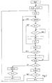
- the first method step consists in determining at least one cause of the error from the degree of error provided by a decoder 2 of the playback device 1 (not shown in FIG. 1). For determining the causes of errors from the degree of error of an optical recording medium 2, with the start of the playback device PLAY, the number of tracks k to be examined with regard to the occurrence of errors and a flag m representing an error rate z are initially set to zero. The number of subcode blocks y is also set to zero when the player PLAY is started. When the first subcode synchronous signal SCOR occurs, the signal flow progresses.
- the number of subcode blocks y per revolution x results from the scanning diameter, which is calculated from the so-called subcode ATIME, multiplied by the number ⁇ , divided by the product of the subcode block time and scanning speed.
- the scanning speed is to be determined only once for each plate in a known manner and the number of subcode blocks y per revolution x is preferably rounded off as an integer.
- the flag m representing the error rate z is set equal to one and then it is waited by increasing the number of subcode blocks y by one whether an error rate z occurs again in the same disk sector.
- the inaccuracy of two subcode blocks y is taken into account in a subsequent step.
- This is followed by an evaluation of defective frames in error packets h.
- a size of the error packets h was selected based on four frames within a subcode block time corresponding to 96 frames, in order to make a distinction between the error causes fingerprint and scratch, black dot in combination with a number of tracks k to be examined for the occurrence of errors enable.
- the repairable cause of the fingerprint error is the first type of error FA1 when more than three error packets h occur in five adjacent tracks k is present.
- scratches and black dots are identified as the second type of error FA2 when up to three error packets h occur in three adjacent tracks k.
- the signal representing the error is linked to a signal equivalent to the disk circulation. This prevents several short disturbances, which do not result from fingerprints, from being added to a signal corresponding to the fingerprint.
- the output signal of the so-called radial detector is preferably used as a signal equivalent to a disk circulation.
- FIG. 6 An arrangement corresponding to this embodiment is shown in FIG. 6. It consists of the player 1, which contains a decoder 2 signaling the degree of error of the optical disc, a processing circuit 3 and a display device 4.
- the processing circuit 3 is connected to the decoder 2, with which the signals representing the degree of error of the optical disc being played are processed . It is a computing unit with which faulty frames are placed in relation to the fault location. As a result of the calculation, one of the possible causes of the fingerprint or scratch, black dot is determined and a related signal is forwarded to the display device 4 connected to the processing circuit 3, which signals the corresponding cause of the error on the display as the first type of error FA1 or second type of error FA2.
- the first method step consists in determining at least the cause of the error fingerprint from the high-frequency signal RF detected by the optical disc with the playback device 1.
- a high-frequency signal RF is schematically shown in FIG. 3, in which the main causes of the error are indicated. It has been found that when the cause of the black dot error occurs, the voltage URF of the radio-frequency signal RF has significant drops, which extend from zero to approximately 10% of the radio-frequency signal RF. As shown in the signal curve, these dips can have different depths and lengths.
- the cause of the error scratches leads to drops in the voltage URF of the high-frequency signal RF, which are characterized by a smaller drop depth and predominantly also a smaller drop length.
- a measurement signal M is derived from the high-frequency signal RF and, when the measurement signal M occurs, within an upper threshold value W1, which was defined as 90% of the high-frequency signal RF, and a lower threshold value W2, which corresponds to 10% of the high-frequency signal RF, the cause of the error fingerprint is determined in a time range with a duration from 4 ms.
- the threshold values W1, W2 By relating the threshold values W1, W2 to peak values A, B of the high-frequency signal RF, independence from the absolute voltage URF of the high-frequency signal RF is achieved. which is device-specific and depends on the quality of the reflective layer of the optical disk.
- their time constant was chosen to be significantly larger than the time constant of the measurement signal M.
- the time constant of the threshold values W1, W2 is 200 ms and that of the measurement signal is 2 ms.
- At least one cause of error is then signaled in a second method step using the display device 4 already mentioned.
- FIG. 4 An arrangement corresponding to FIG. 4 is provided for realizing the execution path starting from the high-frequency signal RF, the block diagram of which is shown in FIG. 5.
- this block diagram has a processing circuit 3 to which a display device 4, which in this case is limited to the cause of the error, is connected.
- the processing circuit 3 is likewise connected to the playback device 1 and, in this embodiment, is connected to the scanner 7 of the playback device 1 that detects the high-frequency signal RF from the optical disk.
- the error display device 5 the internal structure of which is shown in the arrangement corresponding to FIG. 4. This consists of three peak value rectifiers D1, C1, S1; D2, C2, S2; D3, C3, S3, each having a diode D1, D2, D3, a capacitor C1, C2, C3 and a constant current source S1, S2, S3.
- the constant current sources S1, S2, S3 are connected to a ground line or a supply voltage line U1 in accordance with the direction of the diodes D1, D2, D3 and the capacitors C1, C2, C3 are connected to the ground line.
- the diodes D1, D2 of the two first peak value rectifiers D1, C1, S1; D2, C2, S2 are directed in opposite directions and, together with the diode D3 of the second peak value rectifier D3, C3, S3, are connected to the scanner 7 providing the high-frequency signal RF.
- the direction of the diode D3 of the second peak value rectifier D3, C3, S3, with which the measurement signal M is derived from the high frequency signal RF, corresponds to the phase position of the high frequency signal RF and two first comparators V1, V2 are connected to the second peak value rectifier D3, C3, S3.
- a timing element is connected to the output of the gate G and is formed by an integrator with a comparator V3 connected downstream.
- the integrator consists of a diode D4, a constant current source S4, which is connected to a supply voltage U2, and a capacitor C4.
- an integration signal d which is also shown in FIG. 3, is provided and is supplied to the comparator V3 for comparison with the reference voltage U3, so that at the output of the comparator V3 by the reference voltage U 3 Period of 4 ms the error signal, which identifies the cause of the error fingerprint, is emitted.
- a monoflop F for pulse extension is connected to the comparator V3, the display signal f of which is also shown in FIG. 3 and is supplied to a light emitting diode LD, which is the cause of the error Visually displays fingerprint.
- This based on the high-frequency signal RF error display device 5, can be combined analogously to an error display device 5 based on the degree of error, which also consists of a processing circuit 3 and a display device 4, according to FIGS. 5 and 6, with the playback device 1 to form a structural unit 6.
Landscapes
- Engineering & Computer Science (AREA)
- Signal Processing (AREA)
- Optical Recording Or Reproduction (AREA)
- Signal Processing For Digital Recording And Reproducing (AREA)
Applications Claiming Priority (7)
| Application Number | Priority Date | Filing Date | Title |
|---|---|---|---|
| DE4118672 | 1991-06-07 | ||
| DE4118672 | 1991-06-07 | ||
| DE4120870 | 1991-06-25 | ||
| DE4120870 | 1991-06-25 | ||
| DE4210264 | 1992-03-28 | ||
| DE4210264 | 1992-03-28 | ||
| EP92910751A EP0587615B1 (fr) | 1991-06-07 | 1992-05-28 | Signalisation du type de defauts d'un support d'information optique |
Related Parent Applications (2)
| Application Number | Title | Priority Date | Filing Date |
|---|---|---|---|
| EP92910751A Division EP0587615B1 (fr) | 1991-06-07 | 1992-05-28 | Signalisation du type de defauts d'un support d'information optique |
| EP92910751.4 Division | 1992-05-28 |
Publications (2)
| Publication Number | Publication Date |
|---|---|
| EP0671742A1 true EP0671742A1 (fr) | 1995-09-13 |
| EP0671742B1 EP0671742B1 (fr) | 2000-01-12 |
Family
ID=27202565
Family Applications (3)
| Application Number | Title | Priority Date | Filing Date |
|---|---|---|---|
| EP92910751A Expired - Lifetime EP0587615B1 (fr) | 1991-06-07 | 1992-05-28 | Signalisation du type de defauts d'un support d'information optique |
| EP95103711A Expired - Lifetime EP0671742B1 (fr) | 1991-06-07 | 1992-05-28 | Signalisation du type de défauts d'un support d'information optique |
| EP92108998A Pending EP0517099A1 (fr) | 1991-06-07 | 1992-05-28 | Signalisation du genre d'erreurs de porteurs d'enregistrements optiques |
Family Applications Before (1)
| Application Number | Title | Priority Date | Filing Date |
|---|---|---|---|
| EP92910751A Expired - Lifetime EP0587615B1 (fr) | 1991-06-07 | 1992-05-28 | Signalisation du type de defauts d'un support d'information optique |
Family Applications After (1)
| Application Number | Title | Priority Date | Filing Date |
|---|---|---|---|
| EP92108998A Pending EP0517099A1 (fr) | 1991-06-07 | 1992-05-28 | Signalisation du genre d'erreurs de porteurs d'enregistrements optiques |
Country Status (11)
| Country | Link |
|---|---|
| EP (3) | EP0587615B1 (fr) |
| JP (2) | JP3270044B2 (fr) |
| KR (1) | KR100282089B1 (fr) |
| CN (1) | CN1040376C (fr) |
| DE (2) | DE59208917D1 (fr) |
| ES (2) | ES2109357T3 (fr) |
| MY (1) | MY108595A (fr) |
| PT (1) | PT671742E (fr) |
| SG (1) | SG48113A1 (fr) |
| TW (1) | TW207581B (fr) |
| WO (1) | WO1992022064A1 (fr) |
Cited By (1)
| Publication number | Priority date | Publication date | Assignee | Title |
|---|---|---|---|---|
| WO2005047936A3 (fr) * | 2003-11-14 | 2008-02-14 | Lg Electronics Inc | Procede d'evaluation du niveau anti-contamination d'une surface d'un support d'enregistrement optique, appareil et support d'enregistrement optique |
Families Citing this family (5)
| Publication number | Priority date | Publication date | Assignee | Title |
|---|---|---|---|---|
| US6266791B1 (en) * | 1999-02-05 | 2001-07-24 | Hewlett-Packard Company | System and method for selectively recovering areas on a disc marked as unuseable |
| WO2001052249A1 (fr) * | 2000-01-13 | 2001-07-19 | Matsushita Electric Industrial Co., Ltd. | Appareil d'enregistrement/reproduction de disque optique |
| JP3785972B2 (ja) * | 2001-09-06 | 2006-06-14 | ティアック株式会社 | 信号処理回路 |
| ITMI20040985A1 (it) * | 2004-05-17 | 2004-08-17 | Technicolor S P A | Rilevamento automatico di soncronizzazione del suono |
| EP2040258B1 (fr) * | 2006-07-10 | 2010-09-15 | Panasonic Corporation | Dispositif de disque optique |
Citations (10)
| Publication number | Priority date | Publication date | Assignee | Title |
|---|---|---|---|---|
| US287587A (en) * | 1883-10-30 | beainebd spoonee | ||
| DE2851822A1 (de) * | 1978-11-30 | 1980-06-04 | Polygram Gmbh | Verfahren und schaltungsanordnung zur fehlerermittlung bei auf rotierenden informationstraegern in spiralspuren aufgezeichneten signalen |
| EP0073519A2 (fr) * | 1981-08-31 | 1983-03-09 | Sony Corporation | Tourne-disque optique |
| JPS59142756A (ja) * | 1983-02-04 | 1984-08-16 | Sony Corp | 光学式デイスク再生装置 |
| GB2137799A (en) * | 1983-03-15 | 1984-10-10 | Pioneer Electronic Corp | Dirt Detection and Display System for an Information Read-Out System |
| EP0144831A2 (fr) * | 1983-11-17 | 1985-06-19 | POLYGRAM GmbH | Agencement d'appareils pour déterminer des erreurs dans des porteurs d'informations en forme de disques |
| JPS60127574A (ja) * | 1983-12-14 | 1985-07-08 | Toshiba Corp | ドロップアウト検出回路 |
| JPS61242347A (ja) * | 1985-04-19 | 1986-10-28 | Toshiba Corp | 光学式デイスク再生装置 |
| DE3719489A1 (de) * | 1987-06-11 | 1988-12-29 | Thomson Brandt Gmbh | Geraet zur wiedergabe von daten |
| JPH01209344A (ja) * | 1988-02-17 | 1989-08-23 | Seiko Epson Corp | 光ディスク及び光ディスク基板の欠陥検査装置及び欠陥検査方法 |
Family Cites Families (5)
| Publication number | Priority date | Publication date | Assignee | Title |
|---|---|---|---|---|
| US4330881A (en) * | 1980-03-07 | 1982-05-18 | Rca Corporation | Video disc apparatus for clearing foreign matter from the signal pickup stylus during playback |
| JPS62236192A (ja) * | 1986-04-07 | 1987-10-16 | Sony Corp | テ−プ位置検出装置 |
| JPS6332794A (ja) * | 1986-07-25 | 1988-02-12 | Matsushita Electric Ind Co Ltd | 情報再生記録装置 |
| JP2638825B2 (ja) * | 1987-08-06 | 1997-08-06 | オムロン株式会社 | 光カードの記録情報再生装置 |
| DE4029220C2 (de) * | 1990-09-14 | 1999-06-10 | Thomson Brandt Gmbh | Anordnung zur Messung der Bitfehlerrate von Digitalsignalen |
-
1992
- 1992-05-28 EP EP92910751A patent/EP0587615B1/fr not_active Expired - Lifetime
- 1992-05-28 EP EP95103711A patent/EP0671742B1/fr not_active Expired - Lifetime
- 1992-05-28 EP EP92108998A patent/EP0517099A1/fr active Pending
- 1992-05-28 PT PT95103711T patent/PT671742E/pt unknown
- 1992-05-28 ES ES92910751T patent/ES2109357T3/es not_active Expired - Lifetime
- 1992-05-28 JP JP50980992A patent/JP3270044B2/ja not_active Expired - Fee Related
- 1992-05-28 DE DE59208917T patent/DE59208917D1/de not_active Expired - Fee Related
- 1992-05-28 WO PCT/EP1992/001191 patent/WO1992022064A1/fr not_active Ceased
- 1992-05-28 SG SG1996007104A patent/SG48113A1/en unknown
- 1992-05-28 KR KR1019930703797A patent/KR100282089B1/ko not_active Expired - Fee Related
- 1992-05-28 DE DE59209799T patent/DE59209799D1/de not_active Expired - Fee Related
- 1992-05-28 ES ES95103711T patent/ES2142964T3/es not_active Expired - Lifetime
- 1992-06-05 MY MYPI92000980A patent/MY108595A/en unknown
- 1992-06-06 CN CN92104417A patent/CN1040376C/zh not_active Expired - Fee Related
- 1992-06-17 TW TW081104730A patent/TW207581B/zh not_active IP Right Cessation
-
2001
- 2001-09-27 JP JP2001298171A patent/JP3442757B2/ja not_active Expired - Fee Related
Patent Citations (10)
| Publication number | Priority date | Publication date | Assignee | Title |
|---|---|---|---|---|
| US287587A (en) * | 1883-10-30 | beainebd spoonee | ||
| DE2851822A1 (de) * | 1978-11-30 | 1980-06-04 | Polygram Gmbh | Verfahren und schaltungsanordnung zur fehlerermittlung bei auf rotierenden informationstraegern in spiralspuren aufgezeichneten signalen |
| EP0073519A2 (fr) * | 1981-08-31 | 1983-03-09 | Sony Corporation | Tourne-disque optique |
| JPS59142756A (ja) * | 1983-02-04 | 1984-08-16 | Sony Corp | 光学式デイスク再生装置 |
| GB2137799A (en) * | 1983-03-15 | 1984-10-10 | Pioneer Electronic Corp | Dirt Detection and Display System for an Information Read-Out System |
| EP0144831A2 (fr) * | 1983-11-17 | 1985-06-19 | POLYGRAM GmbH | Agencement d'appareils pour déterminer des erreurs dans des porteurs d'informations en forme de disques |
| JPS60127574A (ja) * | 1983-12-14 | 1985-07-08 | Toshiba Corp | ドロップアウト検出回路 |
| JPS61242347A (ja) * | 1985-04-19 | 1986-10-28 | Toshiba Corp | 光学式デイスク再生装置 |
| DE3719489A1 (de) * | 1987-06-11 | 1988-12-29 | Thomson Brandt Gmbh | Geraet zur wiedergabe von daten |
| JPH01209344A (ja) * | 1988-02-17 | 1989-08-23 | Seiko Epson Corp | 光ディスク及び光ディスク基板の欠陥検査装置及び欠陥検査方法 |
Non-Patent Citations (7)
| Title |
|---|
| "MULTI-THRESHOLD SURFACE ANALYSIS TESTER", IBM TECHNICAL DISCLOSURE BULLETIN., vol. 31, no. 8, January 1989 (1989-01-01), NEW YORK US, pages 128 - 130 * |
| GIFFARD: "CD ERROR DETECTOR", ELEKTOR ELECTRONICS., vol. 15, no. 171, October 1989 (1989-10-01), CANTERBURY GB, pages 12 - 15, XP000065732 * |
| KRIEG, BERNHARD: "PRAXIS DER DIGITALEN AUDIOTECHNIK: DIGITALE AUFNAHME UND WIEDERGABE", 1989, FRANZIS-VERLAG, MÜNCHEN, DE * |
| PATENT ABSTRACTS OF JAPAN vol. 11, no. 91 (P - 558) 23 March 1987 (1987-03-23) * |
| PATENT ABSTRACTS OF JAPAN vol. 13, no. 517 (P - 962) 20 November 1989 (1989-11-20) * |
| PATENT ABSTRACTS OF JAPAN vol. 8, no. 275 (P - 321) 15 December 1984 (1984-12-15) * |
| PATENT ABSTRACTS OF JAPAN vol. 9, no. 289 (P - 405)<2012> 15 November 1985 (1985-11-15) * |
Cited By (3)
| Publication number | Priority date | Publication date | Assignee | Title |
|---|---|---|---|---|
| WO2005047936A3 (fr) * | 2003-11-14 | 2008-02-14 | Lg Electronics Inc | Procede d'evaluation du niveau anti-contamination d'une surface d'un support d'enregistrement optique, appareil et support d'enregistrement optique |
| US7536275B2 (en) | 2003-11-14 | 2009-05-19 | Lg Electronics, Inc. | Method for evaluating anti-contamination level on a surface of optical recording medium, the apparatus and the optical recording medium |
| US7571077B2 (en) | 2003-11-14 | 2009-08-04 | Lg Electronics, Inc. | Method for evaluating anti-contamination level on a surface of optical recording medium, the apparatus and the optical recording medium |
Also Published As
| Publication number | Publication date |
|---|---|
| CN1067761A (zh) | 1993-01-06 |
| EP0671742B1 (fr) | 2000-01-12 |
| EP0587615A1 (fr) | 1994-03-23 |
| TW207581B (fr) | 1993-06-11 |
| ES2142964T3 (es) | 2000-05-01 |
| JP2002157844A (ja) | 2002-05-31 |
| EP0587615B1 (fr) | 1997-09-17 |
| JPH06507749A (ja) | 1994-09-01 |
| KR100282089B1 (ko) | 2001-03-02 |
| EP0517099A1 (fr) | 1992-12-09 |
| ES2109357T3 (es) | 1998-01-16 |
| PT671742E (pt) | 2000-04-28 |
| MY108595A (en) | 1996-10-31 |
| JP3442757B2 (ja) | 2003-09-02 |
| CN1040376C (zh) | 1998-10-21 |
| JP3270044B2 (ja) | 2002-04-02 |
| DE59208917D1 (de) | 1997-10-23 |
| SG48113A1 (en) | 1998-04-17 |
| HK1011112A1 (en) | 1999-07-02 |
| KR940701577A (ko) | 1994-05-28 |
| DE59209799D1 (de) | 2000-02-17 |
| WO1992022064A1 (fr) | 1992-12-10 |
Similar Documents
| Publication | Publication Date | Title |
|---|---|---|
| DE69521871T2 (de) | Wiedergabe von optischen Platten | |
| DE69330941T2 (de) | Vorrichtung und verfahren zur plattenaufzeichnung | |
| DE69737346T2 (de) | Verbesserungen an optisch lesbaren platten und plattenaufzeichnungsgerät | |
| DE69930787T2 (de) | Multimedia-System und Verfahren für die automatische Selektion einer Szene | |
| AT404644B (de) | System zum kodieren einer glas-vaterplatte, um eine gefälschte cd-rom zu erkennen | |
| DE3751725T2 (de) | Vorrichtung zur Rückgewinnung der richtigen Spur nach einem Sprung für einen optischen Plattenspieler | |
| DE69733394T2 (de) | Informationsaufzeichnungsträger und Wiedergabeverfahren | |
| DE3303489C2 (fr) | ||
| DE19638161B4 (de) | Aufzeichnungsverfahren für eine Antriebsvorrichtung für eine optische Platte | |
| DE726013T1 (de) | System und verfahren zur wiedergabesteuerung mehrerer, auf einer optischen platte gespeicherter kinofilme | |
| EP0717407B1 (fr) | Appareil de lecture résistant aux vibrations avec synchronisation améliorée | |
| DE69029491T2 (de) | Optische Plattenaufzeichnungs/-wiedergabegerät | |
| DE69324540T2 (de) | Verwaltung einer beschreibbaren Zone für ein Inhaltsverzeichnis sowie Aufzeichnungs- oder Aufzeichnungs-/Wiedergabegerät zum Ausführen einer auf das Inhaltsverzeichnis basierenden Aufzeichnung | |
| DE3233893C2 (de) | Schaltungsanordnung zur Ermittlung des Vorhandenseins eines Informationssignals | |
| DE69124680T2 (de) | Informations-Aufnahme/Wiedergabegerät | |
| DE69932308T2 (de) | Wiedergabegerät für Informationsblöcke enthaltende Aufzeichnungsträger | |
| DE69721644T2 (de) | Informationsaufzeichnungsgerät, -medium und -wiedergabegerät | |
| EP0144831B1 (fr) | Agencement d'appareils pour déterminer des erreurs dans des porteurs d'informations en forme de disques | |
| EP0587615B1 (fr) | Signalisation du type de defauts d'un support d'information optique | |
| DE69228903T2 (de) | Informationswiedergabeverfahren und Informationswiedergabegerät | |
| DE3934631A1 (de) | Wiedergabevorrichtung fuer aufzeichnungen | |
| EP0591842A1 (fr) | Méthode et dispositif pour dissimuler les erreurs de bit et les interpolations dans les signaux sonores numériques | |
| DE68922045T2 (de) | Informationsaufzeichnungsmedium und dasselbe verwendendes Aufzeichnungs/-Wiedergabegerät. | |
| DE69435064T2 (de) | Verfahren und Vorrichtung zur Aufnahme und Wiedergabe digitaler Daten | |
| EP0545945B1 (fr) | Procede de raccourcissement du temps d'acces |
Legal Events
| Date | Code | Title | Description |
|---|---|---|---|
| PUAI | Public reference made under article 153(3) epc to a published international application that has entered the european phase |
Free format text: ORIGINAL CODE: 0009012 |
|
| AC | Divisional application: reference to earlier application |
Ref document number: 587615 Country of ref document: EP |
|
| AK | Designated contracting states |
Kind code of ref document: A1 Designated state(s): DE ES FR GB IT PT |
|
| 17P | Request for examination filed |
Effective date: 19960210 |
|
| 17Q | First examination report despatched |
Effective date: 19960827 |
|
| GRAG | Despatch of communication of intention to grant |
Free format text: ORIGINAL CODE: EPIDOS AGRA |
|
| GRAG | Despatch of communication of intention to grant |
Free format text: ORIGINAL CODE: EPIDOS AGRA |
|
| GRAH | Despatch of communication of intention to grant a patent |
Free format text: ORIGINAL CODE: EPIDOS IGRA |
|
| GRAH | Despatch of communication of intention to grant a patent |
Free format text: ORIGINAL CODE: EPIDOS IGRA |
|
| GRAA | (expected) grant |
Free format text: ORIGINAL CODE: 0009210 |
|
| AC | Divisional application: reference to earlier application |
Ref document number: 587615 Country of ref document: EP |
|
| AK | Designated contracting states |
Kind code of ref document: B1 Designated state(s): DE ES FR GB IT PT |
|
| GBT | Gb: translation of ep patent filed (gb section 77(6)(a)/1977) |
Effective date: 20000112 |
|
| REF | Corresponds to: |
Ref document number: 59209799 Country of ref document: DE Date of ref document: 20000217 |
|
| ET | Fr: translation filed | ||
| ITF | It: translation for a ep patent filed | ||
| REG | Reference to a national code |
Ref country code: PT Ref legal event code: SC4A Free format text: AVAILABILITY OF NATIONAL TRANSLATION Effective date: 20000125 |
|
| REG | Reference to a national code |
Ref country code: ES Ref legal event code: FG2A Ref document number: 2142964 Country of ref document: ES Kind code of ref document: T3 |
|
| PLBE | No opposition filed within time limit |
Free format text: ORIGINAL CODE: 0009261 |
|
| STAA | Information on the status of an ep patent application or granted ep patent |
Free format text: STATUS: NO OPPOSITION FILED WITHIN TIME LIMIT |
|
| 26N | No opposition filed | ||
| REG | Reference to a national code |
Ref country code: GB Ref legal event code: IF02 |
|
| PGFP | Annual fee paid to national office [announced via postgrant information from national office to epo] |
Ref country code: ES Payment date: 20090605 Year of fee payment: 18 |
|
| PGFP | Annual fee paid to national office [announced via postgrant information from national office to epo] |
Ref country code: PT Payment date: 20090522 Year of fee payment: 18 Ref country code: IT Payment date: 20090520 Year of fee payment: 18 Ref country code: FR Payment date: 20090526 Year of fee payment: 18 Ref country code: DE Payment date: 20090525 Year of fee payment: 18 |
|
| PGFP | Annual fee paid to national office [announced via postgrant information from national office to epo] |
Ref country code: GB Payment date: 20090430 Year of fee payment: 18 |
|
| REG | Reference to a national code |
Ref country code: PT Ref legal event code: MM4A Free format text: LAPSE DUE TO NON-PAYMENT OF FEES Effective date: 20101129 |
|
| GBPC | Gb: european patent ceased through non-payment of renewal fee |
Effective date: 20100528 |
|
| REG | Reference to a national code |
Ref country code: FR Ref legal event code: ST Effective date: 20110131 |
|
| PG25 | Lapsed in a contracting state [announced via postgrant information from national office to epo] |
Ref country code: PT Free format text: LAPSE BECAUSE OF NON-PAYMENT OF DUE FEES Effective date: 20101129 |
|
| PG25 | Lapsed in a contracting state [announced via postgrant information from national office to epo] |
Ref country code: IT Free format text: LAPSE BECAUSE OF NON-PAYMENT OF DUE FEES Effective date: 20100528 |
|
| PG25 | Lapsed in a contracting state [announced via postgrant information from national office to epo] |
Ref country code: DE Free format text: LAPSE BECAUSE OF NON-PAYMENT OF DUE FEES Effective date: 20101201 |
|
| PG25 | Lapsed in a contracting state [announced via postgrant information from national office to epo] |
Ref country code: FR Free format text: LAPSE BECAUSE OF NON-PAYMENT OF DUE FEES Effective date: 20100531 |
|
| REG | Reference to a national code |
Ref country code: ES Ref legal event code: FD2A Effective date: 20110708 |
|
| PG25 | Lapsed in a contracting state [announced via postgrant information from national office to epo] |
Ref country code: ES Free format text: LAPSE BECAUSE OF NON-PAYMENT OF DUE FEES Effective date: 20110628 Ref country code: GB Free format text: LAPSE BECAUSE OF NON-PAYMENT OF DUE FEES Effective date: 20100528 |
|
| PG25 | Lapsed in a contracting state [announced via postgrant information from national office to epo] |
Ref country code: ES Free format text: LAPSE BECAUSE OF NON-PAYMENT OF DUE FEES Effective date: 20100529 |