EP0672996A2 - Panneau d'entrée pour éviter des motifs d'interférence - Google Patents
Panneau d'entrée pour éviter des motifs d'interférence Download PDFInfo
- Publication number
- EP0672996A2 EP0672996A2 EP95400591A EP95400591A EP0672996A2 EP 0672996 A2 EP0672996 A2 EP 0672996A2 EP 95400591 A EP95400591 A EP 95400591A EP 95400591 A EP95400591 A EP 95400591A EP 0672996 A2 EP0672996 A2 EP 0672996A2
- Authority
- EP
- European Patent Office
- Prior art keywords
- spacers
- board
- conductive layer
- transparent conductive
- input panel
- Prior art date
- Legal status (The legal status is an assumption and is not a legal conclusion. Google has not performed a legal analysis and makes no representation as to the accuracy of the status listed.)
- Granted
Links
Images


Classifications
-
- G—PHYSICS
- G06—COMPUTING OR CALCULATING; COUNTING
- G06F—ELECTRIC DIGITAL DATA PROCESSING
- G06F3/00—Input arrangements for transferring data to be processed into a form capable of being handled by the computer; Output arrangements for transferring data from processing unit to output unit, e.g. interface arrangements
- G06F3/01—Input arrangements or combined input and output arrangements for interaction between user and computer
- G06F3/03—Arrangements for converting the position or the displacement of a member into a coded form
- G06F3/041—Digitisers, e.g. for touch screens or touch pads, characterised by the transducing means
- G06F3/045—Digitisers, e.g. for touch screens or touch pads, characterised by the transducing means using resistive elements, e.g. a single continuous surface or two parallel surfaces put in contact
-
- G—PHYSICS
- G06—COMPUTING OR CALCULATING; COUNTING
- G06F—ELECTRIC DIGITAL DATA PROCESSING
- G06F3/00—Input arrangements for transferring data to be processed into a form capable of being handled by the computer; Output arrangements for transferring data from processing unit to output unit, e.g. interface arrangements
- G06F3/01—Input arrangements or combined input and output arrangements for interaction between user and computer
- G06F3/03—Arrangements for converting the position or the displacement of a member into a coded form
- G06F3/041—Digitisers, e.g. for touch screens or touch pads, characterised by the transducing means
Definitions
- the present invention generally relates to input devices using an input pen, a touch panel, and the like used in personal computers, word processors, handy terminals, electronic notes, etc., and more particularly relates to an input device of a resistance layer type.
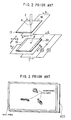
- Figs.1A and 1B show an input panel of a resistance layer type of the prior art.
- the input panel includes a lower board 1 and an upper board 2 which are provided on one surface thereof with transparent conductive layers 3 and 4, respectively. These two boards 1 and 2 are arranged such that the surfaces bearing the transparent conductive layers 3 and 4 face each other. Between the conductive layers 3 and 4, insulating spacers 5 are placed in a dot form or in a mesh form.
- Fig.2 shows a control circuit of the input panel of Fig.l.
- the upper conductive layer 4 is provided with X-coordinate electrodes 17 and 18, and the lower conductive layer 3 is provided with Y-coordinate electrodes 19 and 20. These electrodes are electrically connected as shown in Fig.2.
- This panel can be provided on a display panel of a such device as a liquid crystal display (LCD) device, thus providing means for coordinate input.
- LCD liquid crystal display
- the two conductive layers 3 and 4 are arranged with a short gap therebetween held by the spacers 5, which gap is typically shorter than 14 ⁇ m.
- the spacers 5 which gap is typically shorter than 14 ⁇ m.
- an input panel of a resistance layer type includes a first board having a first transparent conductive layer on one surface thereof, a second board having a second transparent conductive layer on one surface thereof, the first board and the second board being arranged such that the first transparent conductive layer faces the second transparent conductive layer, first spacers arranged between the first board and the second board, the first spacers being non-conductive and having a height no greater than 14 ⁇ m, and second spacers arranged between the first board and the second board among the first spacers, the second spacers being non-conductive and having a height no smaller than 15 ⁇ m.
- the second spacers having a height no smaller than 15 ⁇ m are arranged in a mixture with the smaller first spacers, so that the gap between the conductive layers can be widened to prevent a generation of interference patterns. Also, the smaller first spacers can keep a desirable input characteristic in terms of the input sensitivity, which would be lost when using only the taller second spacers.
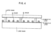
- Fig.4 shows a principle of an input panel according to the present invention.
- the input panel includes a lower board 1, an upper board 2, transparent conductive layers 3 and 4, spacers 5, and other spacers 6.
- the conductive layers 3 and 4 are provided on one surface of the lower board 1 and the upper board 2, respectively, so as to face each other. Between the lower board 1 and the upper board 2, the spacers 5 formed from an insulating material are distributed at constant intervals to hold a constant space between the two boards 1 and 2, and have the same height as those of the prior art, i.e., less than 14 ⁇ m.
- the spacers 6 are arranged between the upper board 2 and the lower board 1 in order to prevent a generation of optical interference.
- the spacers 6 have a greater height than do the spacers 5, which height is more than 15 ⁇ m. Also, the spacers 6 are arranged in a fewer number than that of the spacers 5 so as to be scattered among them.
- Fig.5 shows an illustrative drawing showing a mechanism of the generation of interference patterns.
- Interference patterns are generated by optical interference between two light waves which are transmitted from the same optical source, separated into two different paths and then combined together.
- Fig.5 shows an interference occurring in a thin layer.
- interference occurs between light reflected on the upper surface and light reflected on the lower surface of the thin layer.
- a wavelength of incident light is denoted by ⁇
- D a difference in path lengths between light reflected on the upper surface and light reflected on the lower surface
- the light incident to the thin layer is white light
- a different color can be observed depending on a layer thickness d and an incident angle, since wavelengths of light strengthened by interference are different from wavelengths of light canceled by interference.
- the layer thickness d becomes large, the wavelengths of the light strengthened by interference and the wavelengths of light canceled by interference come close to each other within a small range of wavelengths.
- the wavelengths of light falling within the range are averaged over so that no color can be observed.
- the height of the spacer needs to be 2 to 14 ⁇ m.
- a gap ranging from 2 to 14 ⁇ m is likely to cause the interference by light reflected by the two conductive layers.
- the gap ranging from 2 to 14 ⁇ m is four to thirty times the wavelength of 500 nm, which is about at the middle of a wavelength range of visible light.
- various examinations about gaps have resulted in a finding that a gap larger than 15 ⁇ m is unlikely to generate interference patterns.
- the spacer configuration of the present invention is based on this finding.
- spacers arranged between the two conductive layers 3 and 4 include not only the spacers 5 of the prior art but also the spacers 6 having a height greater than 15 ⁇ m, which is greater than that of the prior art spacers 5.
- the spacers 6 are scattered among the spacers 5 such that the gap between the two conductive layers 3 and 4 is made larger to prevent the generation of interference patterns.
- the spacer 6 for preventing the interference patterns is characterized by its height being greater than 15 ⁇ m, and, also, is characterized in that the spacers 6 are arranged in a smaller number than that of the spacers 5. Preferably, intervals between the spacers 6 range from 0.5 mm to 20 mm.
- Fig.6 shows a flow chart of a method of forming the input panel
- Figs.7A to 7C show process charts of the method.
- the method of forming the input panel will be described.
- the first spacers are formed on a first transparent conductive layer formed on a first board, as shown in Fig.7A.
- the first spacers are non-conductive, and have a height no greater than 14 ⁇ m.
- the second spacers are formed on the first transparent conductive layer, as shown in Fig.7B.
- the second spacers are non-conductive, and have a height no smaller than 15 ⁇ m.
- a second board is placed on the second spacers such that a second transparent conductive layer formed on one surface of the second board faces the first transparent conductive layer, as shown in Fig.7C.
- a method of forming the spacers 6 may be a photolithography method which exposes a photoresist to patterning light and develops it to make a pattern.
- the spacers 6 may be formed by printing a thermoplastic resin, thermosetting resin, or an optical-setting resin in a printing process such as screen printing.
- the spacers 6 may be formed by scattering on the conductive layer small balls or particles made of a resin, an inorganic material, or a combination of inorganic material and organic material.
- these small balls or particles When these small balls or particles are scattered on the conductive layer, they may be coated beforehand by an adhesive resin for sticking them on the conductive layer. In order to position the small balls or particles, a metal mask having holes at predetermined positions may be used such that the small balls or particles are scattered on the metal mask placed on the conductive layer.
- the input panel of the present invention has the spacers 6 greater than 15 ⁇ m arranged among the spacers 5 of the prior art.
- the gap between the two conductive layers 3 and 4 becomes large so as to be able to prevent the generation of the interference patterns.
- the spacers 6 are arranged at the intervals of 0.5 mm to 20 mm, which are wider intervals than those of the prior art spacers 5. Thus, the spacers 6 do not hinder the function of the input panel, and, at the same time, prevent the upper board 2 from bending downward to generate interference patterns.
- the spacers 6 having the height greater than 15 ⁇ m can be formed by a photo process using the photoresist or the printing process using a resin such as the thermoplastic resin, the thermosetting resin, or the optical-setting resin.
- the spacers 6 can be the small balls or particles made of the resin material, the inorganic material, or the combination of organic material and inorganic material, which are coated with the adhesive resin and scattered on the conductive layer. In scattering the small balls or particles, the metal mask having holes at the predetermined locations can be used to arrange the spacers 6 at desired intervals.
- dots having a height of 10 ⁇ m and a size of 70 ⁇ m by 70 ⁇ m are formed at an intervals of 500 ⁇ m by a screen printing process. Then, on the same SnO2 layer, dots having a height of 20 ⁇ m and the size of 70 ⁇ m by 70 ⁇ m are formed at intervals of 4.0 mm by a screen printing process. Both types of dots are arranged on nodes of a respective grid pattern.
- Y-coordinate electrodes are formed on the SnO2 layer.
- X-coordinate electrodes are formed on an ITO (indium tin oxide) layer of a thickness of 175 ⁇ m which is provided on a film. Then an input panel is created by adhering the film to the glass plate such that both conductive layers face each other.
- ITO indium tin oxide
- the input panel is connected to a control circuit, and operations of the panel are examined on an LCD.
- the input panel of the first embodiment provides a suitable input sensitivity.
- Y-coordinate electrodes are formed on the SnO2 layer, and an input panel is created by adhering the glass plate to a film having an ITO layer provided with X-coordinate electrodes.
- Fig.8 shows the input panel of the second embodiment.
- the input panel includes the spacers 5 and spherical spacers 6A for preventing the generation of interference patterns.
- the spherical spacers 6A are stuck to the conductive layer 3 by adhesive resin 7.
- the input panel placed on an LCD. Also, the input panel provides a suitable input sensitivity.
- an SnO2 layer of a thickness of 1.1 mm provided on one surface of a glass plate dots having the height of 10 ⁇ m and the size of 70 ⁇ m by 70 ⁇ m are formed on nodes of a grid pattern at the intervals of 500 ⁇ m by a screen printing process. Then, Y-coordinate electrodes are formed on the SnO2 layer by using a screen printing method. Finally, an input panel is created by adhering the glass plate to a film having an ITO layer (175 ⁇ m of thickness) provided with X coordinate electrodes.
- An input panel of the comparative example 2 differs from that of the comparative example 1 only in the dot height and the intervals.
- the dot height is 3 ⁇ m
- the intervals are 300 ⁇ m.
- the dot height is 14 ⁇ m, and the intervals are 700 ⁇ m.
- the rest is the same as that of the comparative example 1.
- the dot height is 17 ⁇ m, and the intervals are 1.0 mm.
- the rest is the same as that of the comparative example 1.
- the dot height is 17 ⁇ m, and the intervals are 1.5 mm.
- the rest is the same as that of the comparative example 1.
- the spacers with a height no greater than 14 ⁇ m end up generating undesirable interference patterns.
- the spacers of a 17- ⁇ m height and 1.0-mm intervals require a larger hand pressure for entering input compared to the comparative examples 1 to 3. This leads to a poor input sensitivity.
- a good input sensitivity is recovered by widening the spacer intervals to 1.5 mm in the comparative example 5.
- erroneous input by hand tends to be generated in the comparative example 5.
- spacer intervals cannot be found which realize an input sensitivity satisfying both conditions of good pen input and no erroneous inputs.
- the transparent input panel of the resistance layer type according the present invention has the upper and lower boards provided with the transparent conductive layers on the board surfaces facing each other, between which conductive layers the insulating spacers are arranged in the dot form or the mesh form.
- the input panel of the present invention is characterized in that the spacers having a height greater than 15 ⁇ m and the spacers having a height smaller than 14 ⁇ m are arranged in a mixed manner. With this configuration, interference patterns which are generated in a uniform arrangement of the spacers smaller than 14 ⁇ m can be eliminated.
- this input panel when installed on a display, can provide an input capacity as sensitive as that of the prior art, yet eliminate interference patterns which would hinder the clarity of the display.
- the spacers of the height greater than 15 ⁇ m are arranged at the intervals from 0.5 mm to 20 mm, which are wider than the intervals of the spacers of the height smaller than 14 ⁇ m. This arrangement can realize desirable input characteristics in terms of the input sensitivity.
- the photo process using a photoresist or the printing process using the thermoplastic resin, the thermosetting resin, or the optical-setting resin can be employed without a need for a complex process.
- the small balls or particles made of the resin material, the inorganic material, or the combination of the organic material and the inorganic material can be coated with the adhesive resin or the adhesive glass so as to be scattered on the conductive layer in order to form the spacers.
- the spacers can be manufactured in a large number by using simple devices.
- the metal mask having the holes at the predetermined locations can be used to arrange the spacers at the desired intervals.
Landscapes
- Engineering & Computer Science (AREA)
- General Engineering & Computer Science (AREA)
- Theoretical Computer Science (AREA)
- Human Computer Interaction (AREA)
- Physics & Mathematics (AREA)
- General Physics & Mathematics (AREA)
- Position Input By Displaying (AREA)
Applications Claiming Priority (3)
| Application Number | Priority Date | Filing Date | Title |
|---|---|---|---|
| JP49500/94 | 1994-03-18 | ||
| JP4950094A JPH07261907A (ja) | 1994-03-18 | 1994-03-18 | 入力パネル |
| JP4950094 | 1994-03-18 |
Publications (3)
| Publication Number | Publication Date |
|---|---|
| EP0672996A2 true EP0672996A2 (fr) | 1995-09-20 |
| EP0672996A3 EP0672996A3 (fr) | 1996-07-31 |
| EP0672996B1 EP0672996B1 (fr) | 2000-02-02 |
Family
ID=12832869
Family Applications (1)
| Application Number | Title | Priority Date | Filing Date |
|---|---|---|---|
| EP95400591A Expired - Lifetime EP0672996B1 (fr) | 1994-03-18 | 1995-03-17 | Panneau d'entrée de données permettant d'éviter des motifs d'interférence |
Country Status (6)
| Country | Link |
|---|---|
| US (1) | US5668353A (fr) |
| EP (1) | EP0672996B1 (fr) |
| JP (1) | JPH07261907A (fr) |
| KR (1) | KR0154216B1 (fr) |
| DE (1) | DE69514850T2 (fr) |
| TW (1) | TW309604B (fr) |
Families Citing this family (15)
| Publication number | Priority date | Publication date | Assignee | Title |
|---|---|---|---|---|
| JP3442893B2 (ja) * | 1995-01-27 | 2003-09-02 | 富士通株式会社 | 入力装置 |
| JP3249038B2 (ja) * | 1995-11-15 | 2002-01-21 | アルプス電気株式会社 | タブレット一体型液晶表示装置 |
| KR970049350A (ko) * | 1995-12-19 | 1997-07-29 | 윤종용 | 터치패널 |
| US5818430A (en) * | 1997-01-24 | 1998-10-06 | C.A.M. Graphics Co., Inc. | Touch screen |
| US6212852B1 (en) * | 1999-03-15 | 2001-04-10 | Industrial Technology Research Institute | Evacuated glazing containing a thermally insulating vacuum |
| JP4540770B2 (ja) * | 1999-04-23 | 2010-09-08 | 富士通コンポーネント株式会社 | 座標入力装置及び記憶媒体 |
| US6677934B1 (en) | 1999-07-30 | 2004-01-13 | L-3 Communications | Infrared touch panel with improved sunlight rejection |
| US6512512B1 (en) | 1999-07-31 | 2003-01-28 | Litton Systems, Inc. | Touch panel with improved optical performance |
| US6664950B1 (en) * | 1999-11-17 | 2003-12-16 | L-3 Communications | Resistive touch panel using removable, tensioned top layer |
| US7369122B2 (en) * | 2001-12-14 | 2008-05-06 | 3M Innovative Properties Company | Touch panel spacer dots and methods of making |
| JP2004295217A (ja) * | 2003-03-25 | 2004-10-21 | Minebea Co Ltd | タッチパネル |
| JP5361579B2 (ja) * | 2009-07-09 | 2013-12-04 | 信越ポリマー株式会社 | 大型ディスプレイ用のセンサパネル及びその製造方法 |
| US8900027B2 (en) | 2011-05-18 | 2014-12-02 | Eden Park Illumination, Inc. | Planar plasma lamp and method of manufacture |
| TWI469023B (zh) * | 2011-07-21 | 2015-01-11 | Ind Tech Res Inst | 觸控感應裝置 |
| KR20140051005A (ko) * | 2012-10-22 | 2014-04-30 | 삼성디스플레이 주식회사 | 터치스크린패널 |
Family Cites Families (12)
| Publication number | Priority date | Publication date | Assignee | Title |
|---|---|---|---|---|
| US3959585A (en) * | 1974-02-01 | 1976-05-25 | Bell Telephone Laboratories, Incorporated | Graphical input terminal |
| JPS59118040U (ja) * | 1983-01-31 | 1984-08-09 | アルプス電気株式会社 | 入力装置 |
| US4484026A (en) * | 1983-03-15 | 1984-11-20 | Koala Technologies Corporation | Touch tablet data device |
| US4696860A (en) * | 1985-09-26 | 1987-09-29 | John Fluke Mfg. Co., Inc. | Particulate spacers for inhibiting Newton rings in touch sensitive overlays |
| JPH0439613Y2 (fr) * | 1986-05-23 | 1992-09-17 | ||
| JPS6452353A (en) * | 1987-08-07 | 1989-02-28 | Alps Electric Co Ltd | Transparent touch switch |
| US4818827A (en) * | 1988-04-07 | 1989-04-04 | Amp Incorporated | Low force membrane switch |
| JPH02178822A (ja) * | 1988-12-29 | 1990-07-11 | Toppan Moore Co Ltd | 信号入力シート |
| US5172101A (en) * | 1990-10-31 | 1992-12-15 | Bates Joseph P | Omnidirectional input device |
| US5220136A (en) * | 1991-11-26 | 1993-06-15 | Elographics, Inc. | Contact touchscreen with an improved insulated spacer arrangement |
| US5262778A (en) * | 1991-12-19 | 1993-11-16 | Apple Computer, Inc. | Three-dimensional data acquisition on a two-dimensional input device |
| JPH0628088A (ja) * | 1992-07-08 | 1994-02-04 | Fujitsu Ltd | 入力パネルとその製造方法 |
-
1994
- 1994-03-18 JP JP4950094A patent/JPH07261907A/ja active Pending
-
1995
- 1995-03-16 KR KR1019950005478A patent/KR0154216B1/ko not_active Expired - Lifetime
- 1995-03-17 EP EP95400591A patent/EP0672996B1/fr not_active Expired - Lifetime
- 1995-03-17 DE DE69514850T patent/DE69514850T2/de not_active Expired - Lifetime
- 1995-03-17 US US08/406,323 patent/US5668353A/en not_active Expired - Lifetime
- 1995-05-18 TW TW084104945A patent/TW309604B/zh not_active IP Right Cessation
Also Published As
| Publication number | Publication date |
|---|---|
| TW309604B (fr) | 1997-07-01 |
| EP0672996A3 (fr) | 1996-07-31 |
| US5668353A (en) | 1997-09-16 |
| KR0154216B1 (ko) | 1998-11-16 |
| KR950027549A (ko) | 1995-10-18 |
| JPH07261907A (ja) | 1995-10-13 |
| DE69514850T2 (de) | 2000-06-15 |
| EP0672996B1 (fr) | 2000-02-02 |
| DE69514850D1 (de) | 2000-03-09 |
Similar Documents
| Publication | Publication Date | Title |
|---|---|---|
| JP3269628B2 (ja) | 改良された絶縁スペーサ機構をもつコンタクト・タッチスクリーン | |
| EP0672996B1 (fr) | Panneau d'entrée de données permettant d'éviter des motifs d'interférence | |
| EP2401669B1 (fr) | Capteur d'écran tactile et substrat à motifs comprenant des micro-motifs superposés à faible visibilité | |
| KR100816933B1 (ko) | 광역입력가능한 터치패널 | |
| US6814452B2 (en) | Touch-panel with light shielding peripheral part | |
| US10162445B2 (en) | Electrode sheet for pressure detection and pressure detecting module including the same | |
| JP6706239B2 (ja) | タッチ入力装置 | |
| EP3037937B1 (fr) | Dispositif d'entrée tactile | |
| US10429978B2 (en) | Touch panel structure | |
| KR20020072191A (ko) | 뉴튼링 방지필름 및 터치패널 | |
| JP2001154791A (ja) | タッチパネル | |
| EP2713249B1 (fr) | Module d'affichage tactile et appareil électronique portatif | |
| KR20160076298A (ko) | 터치 입력 장치 | |
| CN106681559A (zh) | 触控面板及其制造方法、触控显示装置 | |
| JP2001228975A (ja) | 感圧素子並びにそれを用いたタッチパネル及び液晶表示装置 | |
| DE202011052063U1 (de) | Elektrodenverbindung | |
| US20040239644A1 (en) | Touch panel having colored dot spacers | |
| JPH08241160A (ja) | 透明タッチパネル | |
| JP6465393B2 (ja) | 導電性パターンシートの製造方法、導電性パターンシート、導電性パターンシートを備えたタッチパネルセンサおよびフォトマスク | |
| KR20180052580A (ko) | 전극시트 및 터치 입력 장치 | |
| KR20180029220A (ko) | 압력 검출을 위한 전극시트 및 이를 포함하는 터치 입력 장치 | |
| KR200226352Y1 (ko) | 아이콘 일체형 터치패널 | |
| JP2772118B2 (ja) | タッチパネル及びタッチパネル付ディスプレー | |
| JP2000193806A (ja) | クリアコ―ト板、その製造方法、透明導電板及びパネル型入力装置 | |
| KR20160076490A (ko) | 터치 입력 장치 |
Legal Events
| Date | Code | Title | Description |
|---|---|---|---|
| PUAI | Public reference made under article 153(3) epc to a published international application that has entered the european phase |
Free format text: ORIGINAL CODE: 0009012 |
|
| AK | Designated contracting states |
Kind code of ref document: A2 Designated state(s): DE FR GB |
|
| PUAL | Search report despatched |
Free format text: ORIGINAL CODE: 0009013 |
|
| AK | Designated contracting states |
Kind code of ref document: A3 Designated state(s): DE FR GB |
|
| 17P | Request for examination filed |
Effective date: 19960912 |
|
| GRAG | Despatch of communication of intention to grant |
Free format text: ORIGINAL CODE: EPIDOS AGRA |
|
| 17Q | First examination report despatched |
Effective date: 19990111 |
|
| GRAG | Despatch of communication of intention to grant |
Free format text: ORIGINAL CODE: EPIDOS AGRA |
|
| GRAG | Despatch of communication of intention to grant |
Free format text: ORIGINAL CODE: EPIDOS AGRA |
|
| GRAH | Despatch of communication of intention to grant a patent |
Free format text: ORIGINAL CODE: EPIDOS IGRA |
|
| GRAH | Despatch of communication of intention to grant a patent |
Free format text: ORIGINAL CODE: EPIDOS IGRA |
|
| GRAA | (expected) grant |
Free format text: ORIGINAL CODE: 0009210 |
|
| GRAH | Despatch of communication of intention to grant a patent |
Free format text: ORIGINAL CODE: EPIDOS IGRA |
|
| AK | Designated contracting states |
Kind code of ref document: B1 Designated state(s): DE FR GB |
|
| REF | Corresponds to: |
Ref document number: 69514850 Country of ref document: DE Date of ref document: 20000309 |
|
| ET | Fr: translation filed | ||
| PLBE | No opposition filed within time limit |
Free format text: ORIGINAL CODE: 0009261 |
|
| STAA | Information on the status of an ep patent application or granted ep patent |
Free format text: STATUS: NO OPPOSITION FILED WITHIN TIME LIMIT |
|
| 26N | No opposition filed | ||
| REG | Reference to a national code |
Ref country code: GB Ref legal event code: IF02 |
|
| REG | Reference to a national code |
Ref country code: GB Ref legal event code: 732E |
|
| REG | Reference to a national code |
Ref country code: FR Ref legal event code: TP |
|
| PGFP | Annual fee paid to national office [announced via postgrant information from national office to epo] |
Ref country code: FR Payment date: 20140311 Year of fee payment: 20 |
|
| PGFP | Annual fee paid to national office [announced via postgrant information from national office to epo] |
Ref country code: GB Payment date: 20140312 Year of fee payment: 20 |
|
| PGFP | Annual fee paid to national office [announced via postgrant information from national office to epo] |
Ref country code: DE Payment date: 20140417 Year of fee payment: 20 |
|
| REG | Reference to a national code |
Ref country code: DE Ref legal event code: R071 Ref document number: 69514850 Country of ref document: DE |
|
| REG | Reference to a national code |
Ref country code: GB Ref legal event code: PE20 Expiry date: 20150316 |
|
| PG25 | Lapsed in a contracting state [announced via postgrant information from national office to epo] |
Ref country code: GB Free format text: LAPSE BECAUSE OF EXPIRATION OF PROTECTION Effective date: 20150316 |