EP0674972A1 - Vorrichtung zum chemisch-mechanischen Polieren mit verbesserter Verteilung der Polierzusammensetzung - Google Patents
Vorrichtung zum chemisch-mechanischen Polieren mit verbesserter Verteilung der Polierzusammensetzung Download PDFInfo
- Publication number
- EP0674972A1 EP0674972A1 EP95301342A EP95301342A EP0674972A1 EP 0674972 A1 EP0674972 A1 EP 0674972A1 EP 95301342 A EP95301342 A EP 95301342A EP 95301342 A EP95301342 A EP 95301342A EP 0674972 A1 EP0674972 A1 EP 0674972A1
- Authority
- EP
- European Patent Office
- Prior art keywords
- polishing pad
- groove
- substrate
- polishing
- conditioning
- Prior art date
- Legal status (The legal status is an assumption and is not a legal conclusion. Google has not performed a legal analysis and makes no representation as to the accuracy of the status listed.)
- Granted
Links
Images


Classifications
-
- B—PERFORMING OPERATIONS; TRANSPORTING
- B24—GRINDING; POLISHING
- B24B—MACHINES, DEVICES, OR PROCESSES FOR GRINDING OR POLISHING; DRESSING OR CONDITIONING OF ABRADING SURFACES; FEEDING OF GRINDING, POLISHING, OR LAPPING AGENTS
- B24B37/00—Lapping machines or devices; Accessories
- B24B37/11—Lapping tools
- B24B37/20—Lapping pads for working plane surfaces
- B24B37/26—Lapping pads for working plane surfaces characterised by the shape of the lapping pad surface, e.g. grooved
Definitions
- the present invention relates to the field of chemical mechanical polishing. More particularly, the present invention relates to methods and apparatus for chemically mechanically polishing substrates, such as semiconductor substrates, on a rotating polishing pad in the presence of a chemically active and/or physically abrasive slurry, and providing a fresh supply of slurry onto the face of the substrate engaged on the polishing pad as the substrate is being polished. Additionally, the invention may include a pad conditioning apparatus to condition the polishing pad while the pad is being used to polish substrates.
- Chemical mechanical polishing is a method of polishing materials, such as semiconductor substrates, to a high degree of planarity and uniformity. The process is used to planarize semiconductor slices prior to the fabrication of microelectronic circuitry thereon, and is also used to remove high elevation features created during the fabrication of the microelectronic circuitry on the substrate.
- One typical chemical mechanical polishing process uses a large polishing pad, located on a rotating platen, against which a substrate is positioned for polishing, and a positioning member which biases and positions the substrate on the rotating polishing pad.
- a chemical slurry which may also include abrasive materials therein, is maintained on the polishing pad to modify the polishing characteristics of the polishing pad to enhance the polishing of the substrate.
- the slurry is primarily used to enhance the material removal rate of selected materials from the substrate surface.
- the fixed volume of slurry becomes less reactive and the polishing enhancing characteristics of that fixed volume of slurry are significantly reduced.
- One approach to overcoming this problem is to continuously provide fresh slurry onto the polishing pad. This approach presents at least two difficulties.
- One method allows the substrate to "float" on the polishing pad.
- the object of floating the substrate on the polishing pad is to provide a very small downwardly directed force at the substrate-polishing pad interface, so that slurry will flow between the substrate and the polishing pad.
- This method is ineffective because the slurry is still substantially prevented from moving under the substrate by surface tension and other factors, and the use of a low force at the substrate-polishing pad interface substantially increases the cycle time necessary to polish a substrate.
- Another method of providing slurry to the face of the substrate engaged against the polishing pad uses a plurality of holes in the platen, and the slurry is injected through the holes and underside of the polishing pad.
- the object of this method is to ensure that the slurry is constantly replenished at the substrate-polishing pad interface through the underside of the polishing pad.
- this method does provide slurry to the face of the substrate engaged against the polishing pad, it has several drawbacks.
- the primary problem encountered when using this method is that the slurry is injected over the entire area of the polishing pad. Therefore, substantial areas of slurry wetted polishing pad are exposed to the ambient environment, and the slurry that is exposed to the environment tends to dry and glaze the surface of the polishing pad. This glazing significantly reduces the ability of the pad to polish the substrate, and therefore reduces the effectiveness of the polishing equipment.
- a further method of providing slurry to the substrate-polishing pad is shown in United States Patent Number 5,216,843.
- a plurality of concentric, circular grooves which have a center that is co-terminus with the axis of rotation of the polishing pad, are provided in the upper surface of the polishing pad.
- radial "microgrooves" are continuously formed in the surface of the polishing pad by a pad conditioning apparatus. The microgrooves serve to condition the polishing pad surface. Both the polishing pad and the substrate rotate as the substrate is processed. Because the substrate rotates, all areas on the surface of the substrate will pass over one, or more, of the grooves during each substrate rotation.
- the slurry is still non-uniformly replenished on the substrate.
- zones of high and low slurry replenishment will occur on the face of the substrate because different areas on the substrate will pass over different numbers of grooves as the substrate rotates.
- the relative distribution of fresh slurry will vary as the distance on the substrate from a groove increases from the nominal position of the substrate on the polishing pad. Therefore, the frequency at which fresh slurry reaches each location on the substrate varies across the face of the substrate, which leads to zones of high and low material removal on the substrate.
- the substrate is linearly or arcuately reciprocated over a distance less than one-half of the spacing between the concentric grooves, portions of the substrate will not come into contact with any groove area, and thus discrete areas of very low slurry replenishment will occur on the substrate.
- the polishing characteristics of the polishing pad also are affected by glazing and compression of the polishing pad surface.
- This glazing and compression are natural by-products of the polishing process and typically cause open cells on the polishing pad surface to close by (i) compression or (ii) filling with polished substrate particulates and dried slurry.
- the present invention is a chemical mechanical polishing apparatus in which slurry is continuously replenished to the face of the substrate engaged against the polishing pad while simultaneously polishing a substrate on the polishing pad.
- the polishing pad of the chemical mechanical polishing apparatus is rotated under the substrate, and at least one groove is provided in the polishing pad and extends therein at least partially in a radial direction.
- the groove provides fresh slurry under the substrate as the groove passes under the substrate, irrespective of the relative motion of the substrate on the polishing pad.
- the groove preferably begins adjacent the center of the pad and radiates outwardly therefrom to the substrate edge and may be curved to form a spiral groove.
- one or more circular grooves may be provided to distribute the slurry to the face of the substrate engaged against the polishing pad.
- the groove sweeps under the substrate and deposits fresh slurry on the face of the substrate engaged on the polishing pad.
- the polishing apparatus includes a pad conditioning member, which provides constant conditioning of the pad to continuously maintain a fresh polishing pad surface on the polishing pad.
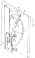
- the polishing apparatus 10 generally includes a base 20 which supports a rotary platen 22 thereon, a polishing pad 14 received on the platen 22, a carrier 24 which positions and selectively loads the substrate 12 against the polishing pad 14, and a drive assembly 46 which drives the carrier 24 to move the substrate on the polishing pad 14.
- the carrier 24 includes a recess, which includes a mounting pad 25 against which the substrate 12 is maintained during polishing.
- the polishing pad 14 is preferably sized up to a 30 cm radius and includes one or more grooves 26 therein to provide fresh slurry to the face of the substrate 12 engaged against the polishing pad 14.
- the slurry may be provided to the polishing pad 14 through a slurry port 27, or through the underside of the polishing pad 14.
- the groove 26 extends at least partially in a radial direction in the surface of the polishing pad 14 for a distance sufficient to ensure that it extends from the radially innermost to the radially outermost position of the substrate 12 on the pad 14. As shown in Figure 1, the groove may extend entirely radially, i.e., in a straight line path along a radius extending outwardly from the center of the polishing pad 22. Additionally, the groove may extend in a straight line, but not along a radius extending from the center of the polishing pad 22, and thus will extend both radially, and circumferentially but not arcuately, in the polishing pad 22.
- the composition of the polishing pad 14 is preferably a woven polyeurethane material, such as IC 1000 or Suba IV, which is available from Rodel of Newark, Pennsylvania.
- the slurry is selected to enhance the polishing characteristics of the polishing pad 14 and may include components to selectively increase the polishing of one or more of the materials disposed on the substrate 12 surface.
- One slurry composition which provides enhanced selective polishing of materials deposited on the substrate 12 surface is an aqueous solution having 5% NaOH, 5% KOH, and colloidal silica having a size of approximately 200 nm. Those skilled in the art may easily vary the polishing pad 14 material, and the slurry composition, to provide the desired polishing of the substrate 12 surface.
- the polishing pad 14 includes at least one spiral groove 26a therein, which extends outwardly from the axis of rotation 11 of the polishing pad in both a radial and circumferential direction and terminates adjacent the edge 13 of the polishing pad 14.
- the spiral groove 26a forms a spiral pattern on the polishing pad 14 and is approximately 3.2 mm wide, at least .5 mm deep, and has a spiral pitch of 12.5 to 25 mm.
- the spiral groove 26a is preferably machined into the polishing pad 14, such as by milling, or it may be stamped into, or otherwise formed in, the pad 14.
- the spiral groove 26a is shown extending in a counterclockwise direction, i.e., tracing the groove 26a inward to the center of the polishing pad 14 in a counterclockwise path.
- the spiral groove 26a may extend in a clockwise direction.
- the direction of the spiral groove 26a may be varied with respect to the rotary direction of the polishing pad 14.
- the spiral groove 26a centripetally accelerates the slurry outwardly from the center of the pad and along the underside of the substrate 12.
- the spiral groove 26a scoops slurry under the substrate 12.
- spiral groove 26a is described as having a pitch of approximately 12.5 to 25 mm on a polishing pad 14 having a 30 cm radius, the spiral groove 26a is useful at substantially greater and smaller pitches. Additionally, multiple spiral grooves 26a having the same direction and pitch may be used. Multiple spiral grooves 26a may also be provided in opposite directions to provide a sunburst pattern on the polishing pad 14. Further, spiral or circular arcuate groove segments 26c, disposed in a clockwise, counterclockwise, or overlapping clockwise and counterclockwise configuration may be used. One configuration of the overlapping circular arcuate groove segments 26c is shown in Figure 3. The arcuate groove segments 26c preferably extend a sufficient radial distance across the face of the polishing pad 14 to ensure that the arcuate groove segments 26c can replenish slurry at all areas of the substrate 12 which come into contact with the polishing pad 14.
- the polishing pad 14 includes a circular offset groove 26b therein.
- the circular offset groove 26b extends entirely around the polishing pad 14 upper surface, but the center of the circular arc defining the circular offset groove 26b is offset from the axis of rotation 11 of the polishing pad 14. Therefore, at any fixed reference point with respect to the apparatus base 20, the circular offset groove 26b will appear to move radially inwardly and outwardly as the polishing pad 14 rotates.
- the polishing pad 14 is useful with only one circular offset groove 26b, a plurality of concentric circular offset grooves 26b as shown in Figure 5 is preferred.
- the circular offset grooves 26b must be spaced so that the maximum and minimum radial positions of the circular offset grooves 26b will extend slightly beyond the positional limits of the substrate 12 on the polishing pad 14, to ensure that slurry is replenished at all areas of the substrate 12 as the polishing pad 14 rotates.
- the groove configurations provided herein all provide enhanced slurry distribution under a substrate 12 on a rotating polishing pad 14, and are useful where the substrate 12 is rotated, vibrated, orbited or otherwise moved on the polishing pad 14. Because the grooves in the polishing pad of the present invention extend radially in the polishing pad, slurry maintained on the polishing pad 14 or in any of the grooves configurations will pass under the substrate 12 to continuously provide fresh slurry to all areas of the substrate 12 as it is polished, irrespective of the motion of the substrate 12 on the polishing pad 14. Therefore, the polishing pad 14 configuration of the present invention is particularly suited to applications where the substrate does not rotate, or rotates at a very small speed.
- the polishing pad configuration of the present invention enables the use of orbital substrate motion, or reciprocating linear or arcuate substrate motion such as vibration or oscillation while ensuring that the slurry replenishment effect of the groove configurations will not create areas of high and low slurry replenishment on the substrate 12.
- FIG. 1 the general configuration of an orbital drive system 48 with controlled rotation is shown for orbiting a carrier 24, and a substrate 12 received therein.
- the orbital drive system 48 generally includes a drive motor 76 configured to provide orbital motion to the carrier 24, a control motor 78 configured to provide selective rotary motion to the carrier 24 as it orbits, and a drive assembly 48 coupled to the drive motor 76 and control motor 78, and to the carrier 24, and configured to convert rotational motion of the drive motor 76 and control motor 78 into orbital and controlled rotational motion of the carrier 24.
- a drive motor 76 configured to provide orbital motion to the carrier 24
- control motor 78 configured to provide selective rotary motion to the carrier 24 as it orbits
- a drive assembly 48 coupled to the drive motor 76 and control motor 78, and to the carrier 24, and configured to convert rotational motion of the drive motor 76 and control motor 78 into orbital and controlled rotational motion of the carrier 24.
- the rotational and orbital motion of the carrier 24, in addition to the rotational motion of the polishing pad 14, provide a relative velocity at the face of the substrate 12 engaged on the polishing pad 14 of 1800 to 4800 cm/min. Additionally, it is preferred that the rotational speed of the polishing pad 14 is no more than 10 rpm, preferably 5 rpm, and that the orbital radius of the substrate 12 is no more than one inch.
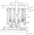
- the carrier 24 is orbitally driven by a drive assembly 46 suspended from crossbar 36, and rotationally controlled by a compensation assembly 80 formed in the drive assembly 46.
- the drive assembly 46 includes a rotatable drive shaft 38, and a housing 40 suspended on the crossbar 36 through which the drive shaft 38 extends.
- the housing 40 includes an inner fixed hub 70 which is connected to the crossbar 36 to rigidly fix the housing 40 to the crossbar 36, and an outer rotatable hub 72 received over the fixed hub 70 on bearings.
- the outer hub 72 is coupled to the control motor 78 by a drive beit as best shown in Figure 1.
- the drive shaft 38 extends through the inner fixed hub 70 and is supported therein on bearings.
- the upper end of the drive shaft 38 extends above the cross arm 36 and is coupled to the drive motor 76 by a drive belt, as best shown in Figure 1.
- the lower end of the drive shaft 38 extends below the housing 40.
- One end of a cross arm 42 is received on the lower end of the drive shaft 38, and a second shaft 44 is received in the opposite end of the cross arm 42 and extends downwardly therefrom.
- the lower end of the second shaft 42 engages the carrier 24 to transmit orbital motion into the carrier 24.
- the drive shaft 38 When the drive shaft 38 is rotated by the drive motor 76, it sweeps the cross arm 42 in a circular path which in turn moves the second shaft 44 and the carrier 24 attached thereto through an orbital path.
- the radius of this path is equal to the distance between the center of the drive shaft 38 and the center of the second shaft 44 at the cross arm 42.
- the lower end of the second shaft 44 is preferably a low friction coupling member, which is received in a mating coupling in the carrier 24 to impart minimal rotation to the carrier 24 or the substrate 12 therein.
- the coupling of the second shaft 44 to the carrier 24, as well as the substrate 12 in the carrier 24 to the polishing pad 14 is frictionless, the substrate 12 may move in a rotational direction as it passes through the orbital path.
- the lower end of the housing 40 is configured as the compensation assembly 80.
- This compensation assembly 80 includes a ring gear 50 provided about the inner perimeter of the base of the outer hub 72 of the housing 40, and a pinion gear 52 provided on the upper end of the second shaft 44 adjacent the cross arm 42.
- the pinion gear 52 is meshed with the ring gear 50, and is also coupled via a plurality of free floating pins 56 to the carrier 24.
- the speed of rotation of the carrier 24 may be matched to, or varied from, the speed of rotation of the polishing pad 14 by simply changing the relative rotational speeds of the drive shaft 38 and the outer rotatable hub 72 of the housing 40.
- a polishing pad 14 having grooves which extend at least partially in a radial direction provides constant replenishment of slurry on the substrate 12 surface engaged against the polishing pad 14.
- an annular region of compressed or filled polishing pad 14 material forms where the substrate 12 engages the polishing pad 14.
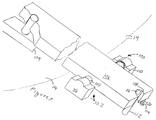
- a pad conditioning apparatus 100 is shown for continuously conditioning the polishing pad 14 by abrading the surface thereof during processing of substrates 12 thereon.
- the pad conditioning apparatus 100 includes a mounting assembly 102, which positions a pad conditioning bar 104 on the polishing pad 14 as the polishing pad 14 rotates.
- the mounting assembly 102 includes a generally longitudinal support bar 106, which is supported on a shaft 108.
- the ends of the shaft 108 are received in a pair of cushioned pillow blocks 110, which are mounted to the apparatus 10 base.
- the pillow blocks 110 preferably include a metal shell with conformable sleeves therein for receiving the ends of the shaft 108. The sleeves dampen any oscillatory motion of the shaft 108 to increase the life of the pillow block 110.
- the pillow block 110 serves as a pivot for the support bar 106.
- a vibratory assembly 112 and a loading member 114 are provided in contact with the support bar 106.
- the vibratory assembly 112 includes an offset rod 116, which extends into a circular aperture 118 in the bar 106.
- the rod 116 is rotated at a high speed around an axis which is offset from its longitudinal axis. Therefore, a portion of the rod 116 will engage and disengage from the wall of the aperture 118, which will cause the support bar 106 to vibrate.
- the loading member 114 is preferably a pneumatic piston, mounted in the apparatus base, which includes a piston rod 120 that engages against the underside of the support bar 106 to downwardly bias the opposite end of the support bar 106.
- the support bar 106 extends from the pillow blocks 110 over the polishing pad 14 to a radial position located to pass the area of the polishing pad 14 conditioned by the conditioning apparatus 100 under the substrate 12 as it is polished on the polishing pad 14.
- the conditioning bar 104 is mounted to the end of the support bar 106 and contacts the polishing pad 14.
- a 600 grit silica, or other abrasive, is provided on the underside of the conditioning bar 104 to engage the upper surface of the polishing pad 14 as the polishing pad rotates thereunder.
- the conditioning bar 104 is slightly longer that the circumference of the substrate 12 so that the abrasive will condition an annular area larger that the circumference of the substrate 12.
- the polishing pad 14 is continuously conditioned as it polishes a substrate 12, which eliminates the need to separately condition the polishing pad 14 after one or more substrates have been polished thereon.
- the conditioning bar 104 is described as using an abrasive silica grit, other materials such as diamond tipped pins, blades or other abrasives may be used to condition the polishing pad 14.
- inventions described herein may be used concurrently, or independently, to maximize the uniformity and rate at which substrates are polished.
Landscapes
- Engineering & Computer Science (AREA)
- Mechanical Engineering (AREA)
- Finish Polishing, Edge Sharpening, And Grinding By Specific Grinding Devices (AREA)
- Mechanical Treatment Of Semiconductor (AREA)
Applications Claiming Priority (2)
| Application Number | Priority Date | Filing Date | Title |
|---|---|---|---|
| US205278 | 1994-03-02 | ||
| US08/205,278 US5650039A (en) | 1994-03-02 | 1994-03-02 | Chemical mechanical polishing apparatus with improved slurry distribution |
Publications (2)
| Publication Number | Publication Date |
|---|---|
| EP0674972A1 true EP0674972A1 (de) | 1995-10-04 |
| EP0674972B1 EP0674972B1 (de) | 1998-07-15 |
Family
ID=22761558
Family Applications (1)
| Application Number | Title | Priority Date | Filing Date |
|---|---|---|---|
| EP95301342A Expired - Lifetime EP0674972B1 (de) | 1994-03-02 | 1995-03-02 | Vorrichtung zum chemisch-mechanischen Polieren mit verbesserter Verteilung der Polierzusammensetzung |
Country Status (6)
| Country | Link |
|---|---|
| US (1) | US5650039A (de) |
| EP (1) | EP0674972B1 (de) |
| JP (1) | JPH0839423A (de) |
| KR (1) | KR950031381A (de) |
| AT (1) | ATE168306T1 (de) |
| DE (1) | DE69503408T2 (de) |
Cited By (11)
| Publication number | Priority date | Publication date | Assignee | Title |
|---|---|---|---|---|
| EP0763402A1 (de) * | 1995-09-08 | 1997-03-19 | Matsushita Electric Industrial Co., Ltd. | Verfahren und Vorrichtung zum Polieren von Halbleitersubstraten |
| EP0770455A1 (de) * | 1995-10-27 | 1997-05-02 | Applied Materials, Inc. | Ein Abrichtgerät für ein chemisch-mechanisches Poliersystem |
| EP0803327A3 (de) * | 1996-04-26 | 1998-08-19 | MEMC Electronic Materials, Inc. | Vorrichtung und Verfahren zum Formen von Polierkissen |
| US5851136A (en) * | 1995-05-18 | 1998-12-22 | Obsidian, Inc. | Apparatus for chemical mechanical polishing |
| US6019670A (en) * | 1997-03-10 | 2000-02-01 | Applied Materials, Inc. | Method and apparatus for conditioning a polishing pad in a chemical mechanical polishing system |
| EP0878270A3 (de) * | 1997-05-15 | 2000-08-23 | Applied Materials, Inc. | Polierkissen mit Rillenmuster zur Verwendung in einer chemisch-mechanischen Poliervorrichtung |
| US6488565B1 (en) | 2000-08-29 | 2002-12-03 | Applied Materials, Inc. | Apparatus for chemical mechanical planarization having nested load cups |
| EP1329290A3 (de) * | 1999-05-21 | 2003-07-30 | Lam Research Corporation | Polierkissen mit Rillenmuster zur Verwendung in einer chemisch-mechanischen Poliervorrichtung |
| WO2006020153A3 (en) * | 2004-07-21 | 2006-04-27 | Neopad Technologies Corp | Methods for producing in-situ grooves in chemical mechanical planarization (cmp) pads, and novel cmp pad designs |
| US7704125B2 (en) | 2003-03-24 | 2010-04-27 | Nexplanar Corporation | Customized polishing pads for CMP and methods of fabrication and use thereof |
| US8864859B2 (en) | 2003-03-25 | 2014-10-21 | Nexplanar Corporation | Customized polishing pads for CMP and methods of fabrication and use thereof |
Families Citing this family (70)
| Publication number | Priority date | Publication date | Assignee | Title |
|---|---|---|---|---|
| US5709593A (en) | 1995-10-27 | 1998-01-20 | Applied Materials, Inc. | Apparatus and method for distribution of slurry in a chemical mechanical polishing system |
| US6056851A (en) * | 1996-06-24 | 2000-05-02 | Taiwan Semiconductor Manufacturing Company | Slurry supply system for chemical mechanical polishing |
| US6328642B1 (en) | 1997-02-14 | 2001-12-11 | Lam Research Corporation | Integrated pad and belt for chemical mechanical polishing |
| US5944583A (en) * | 1997-03-17 | 1999-08-31 | International Business Machines Corporation | Composite polish pad for CMP |
| US6273806B1 (en) | 1997-05-15 | 2001-08-14 | Applied Materials, Inc. | Polishing pad having a grooved pattern for use in a chemical mechanical polishing apparatus |
| US6030487A (en) * | 1997-06-19 | 2000-02-29 | International Business Machines Corporation | Wafer carrier assembly |
| US5957754A (en) * | 1997-08-29 | 1999-09-28 | Applied Materials, Inc. | Cavitational polishing pad conditioner |
| JPH11216663A (ja) * | 1998-02-03 | 1999-08-10 | Sony Corp | 研磨パッド、研磨装置および研磨方法 |
| US6015499A (en) * | 1998-04-17 | 2000-01-18 | Parker-Hannifin Corporation | Membrane-like filter element for chemical mechanical polishing slurries |
| US6106662A (en) * | 1998-06-08 | 2000-08-22 | Speedfam-Ipec Corporation | Method and apparatus for endpoint detection for chemical mechanical polishing |
| US6135865A (en) | 1998-08-31 | 2000-10-24 | International Business Machines Corporation | CMP apparatus with built-in slurry distribution and removal |
| US6203407B1 (en) | 1998-09-03 | 2001-03-20 | Micron Technology, Inc. | Method and apparatus for increasing-chemical-polishing selectivity |
| US6235635B1 (en) | 1998-11-19 | 2001-05-22 | Chartered Semiconductor Manufacturing Ltd. | Linear CMP tool design using in-situ slurry distribution and concurrent pad conditioning |
| US6589105B2 (en) | 1998-12-01 | 2003-07-08 | Nutool, Inc. | Pad tensioning method and system in a bi-directional linear polisher |
| US6103628A (en) * | 1998-12-01 | 2000-08-15 | Nutool, Inc. | Reverse linear polisher with loadable housing |
| US6468139B1 (en) | 1998-12-01 | 2002-10-22 | Nutool, Inc. | Polishing apparatus and method with a refreshing polishing belt and loadable housing |
| US6409904B1 (en) | 1998-12-01 | 2002-06-25 | Nutool, Inc. | Method and apparatus for depositing and controlling the texture of a thin film |
| US7204917B2 (en) * | 1998-12-01 | 2007-04-17 | Novellus Systems, Inc. | Workpiece surface influencing device designs for electrochemical mechanical processing and method of using the same |
| US6328872B1 (en) | 1999-04-03 | 2001-12-11 | Nutool, Inc. | Method and apparatus for plating and polishing a semiconductor substrate |
| US7425250B2 (en) * | 1998-12-01 | 2008-09-16 | Novellus Systems, Inc. | Electrochemical mechanical processing apparatus |
| US6464571B2 (en) | 1998-12-01 | 2002-10-15 | Nutool, Inc. | Polishing apparatus and method with belt drive system adapted to extend the lifetime of a refreshing polishing belt provided therein |
| US6273797B1 (en) * | 1999-11-19 | 2001-08-14 | International Business Machines Corporation | In-situ automated CMP wedge conditioner |
| US20020068516A1 (en) * | 1999-12-13 | 2002-06-06 | Applied Materials, Inc | Apparatus and method for controlled delivery of slurry to a region of a polishing device |
| KR100575857B1 (ko) * | 1999-12-29 | 2006-05-03 | 주식회사 하이닉스반도체 | 반도체 제조용 연마판 |
| US6630059B1 (en) * | 2000-01-14 | 2003-10-07 | Nutool, Inc. | Workpeice proximity plating apparatus |
| US6241596B1 (en) | 2000-01-14 | 2001-06-05 | Applied Materials, Inc. | Method and apparatus for chemical mechanical polishing using a patterned pad |
| US6579797B1 (en) * | 2000-01-25 | 2003-06-17 | Agere Systems Inc. | Cleaning brush conditioning apparatus |
| US20090020437A1 (en) * | 2000-02-23 | 2009-01-22 | Basol Bulent M | Method and system for controlled material removal by electrochemical polishing |
| JP2002200555A (ja) * | 2000-12-28 | 2002-07-16 | Ebara Corp | 研磨工具および該研磨工具を具備したポリッシング装置 |
| US6609961B2 (en) | 2001-01-09 | 2003-08-26 | Lam Research Corporation | Chemical mechanical planarization belt assembly and method of assembly |
| US6620031B2 (en) | 2001-04-04 | 2003-09-16 | Lam Research Corporation | Method for optimizing the planarizing length of a polishing pad |
| US6837779B2 (en) * | 2001-05-07 | 2005-01-04 | Applied Materials, Inc. | Chemical mechanical polisher with grooved belt |
| KR20030015567A (ko) * | 2001-08-16 | 2003-02-25 | 에스케이에버텍 주식회사 | 웨이브 형태의 그루브가 형성된 화학적 기계적 연마패드 |
| US7314402B2 (en) * | 2001-11-15 | 2008-01-01 | Speedfam-Ipec Corporation | Method and apparatus for controlling slurry distribution |
| US6939203B2 (en) * | 2002-04-18 | 2005-09-06 | Asm Nutool, Inc. | Fluid bearing slide assembly for workpiece polishing |
| US9278424B2 (en) | 2003-03-25 | 2016-03-08 | Nexplanar Corporation | Customized polishing pads for CMP and methods of fabrication and use thereof |
| US6783436B1 (en) | 2003-04-29 | 2004-08-31 | Rohm And Haas Electronic Materials Cmp Holdings, Inc. | Polishing pad with optimized grooves and method of forming same |
| JP4292025B2 (ja) | 2003-05-23 | 2009-07-08 | Jsr株式会社 | 研磨パッド |
| US7442116B2 (en) | 2003-11-04 | 2008-10-28 | Jsr Corporation | Chemical mechanical polishing pad |
| US7125318B2 (en) * | 2003-11-13 | 2006-10-24 | Rohm And Haas Electronic Materials Cmp Holdings, Inc. | Polishing pad having a groove arrangement for reducing slurry consumption |
| US7648622B2 (en) * | 2004-02-27 | 2010-01-19 | Novellus Systems, Inc. | System and method for electrochemical mechanical polishing |
| KR20060046093A (ko) * | 2004-05-20 | 2006-05-17 | 제이에스알 가부시끼가이샤 | 화학 기계 연마 패드 및 화학 기계 연마 방법 |
| US7329174B2 (en) | 2004-05-20 | 2008-02-12 | Jsr Corporation | Method of manufacturing chemical mechanical polishing pad |
| JP2005340271A (ja) * | 2004-05-24 | 2005-12-08 | Jsr Corp | 化学機械研磨用パッド |
| US7198549B2 (en) * | 2004-06-16 | 2007-04-03 | Cabot Microelectronics Corporation | Continuous contour polishing of a multi-material surface |
| DE602005007125D1 (de) | 2004-09-17 | 2008-07-10 | Jsr Corp | Chemisch-mechanisches Polierkissen und chemisch-mechanisches Polierverfahren |
| US7059950B1 (en) | 2004-12-14 | 2006-06-13 | Rohm And Haas Electronic Materials Cmp Holdings, Inc. | CMP polishing pad having grooves arranged to improve polishing medium utilization |
| US7059949B1 (en) | 2004-12-14 | 2006-06-13 | Rohm And Haas Electronic Materials Cmp Holdings, Inc. | CMP pad having an overlapping stepped groove arrangement |
| US7182677B2 (en) * | 2005-01-14 | 2007-02-27 | Applied Materials, Inc. | Chemical mechanical polishing pad for controlling polishing slurry distribution |
| JP2007103602A (ja) * | 2005-10-03 | 2007-04-19 | Toshiba Corp | 研磨パッド及び研磨装置 |
| US7226345B1 (en) | 2005-12-09 | 2007-06-05 | The Regents Of The University Of California | CMP pad with designed surface features |
| KR100882045B1 (ko) * | 2006-02-15 | 2009-02-09 | 어플라이드 머티어리얼스, 인코포레이티드 | 그루브형 서브패드를 구비한 폴리싱 장치 |
| US7300340B1 (en) | 2006-08-30 | 2007-11-27 | Rohm and Haas Electronics Materials CMP Holdings, Inc. | CMP pad having overlaid constant area spiral grooves |
| JP2008290197A (ja) * | 2007-05-25 | 2008-12-04 | Nihon Micro Coating Co Ltd | 研磨パッド及び方法 |
| US7544115B2 (en) * | 2007-09-20 | 2009-06-09 | Novellus Systems, Inc. | Chemical mechanical polishing assembly with altered polishing pad topographical components |
| JP2009220265A (ja) * | 2008-02-18 | 2009-10-01 | Jsr Corp | 化学機械研磨パッド |
| US9180570B2 (en) | 2008-03-14 | 2015-11-10 | Nexplanar Corporation | Grooved CMP pad |
| TWI409137B (zh) * | 2008-06-19 | 2013-09-21 | Bestac Advanced Material Co Ltd | 研磨墊及其微型結構形成方法 |
| TWI449597B (zh) * | 2008-07-09 | 2014-08-21 | Iv Technologies Co Ltd | 研磨墊及其製造方法 |
| TWM352127U (en) * | 2008-08-29 | 2009-03-01 | Bestac Advanced Material Co Ltd | Polishing pad |
| TWM352126U (en) * | 2008-10-23 | 2009-03-01 | Bestac Advanced Material Co Ltd | Polishing pad |
| KR20110104007A (ko) | 2008-12-09 | 2011-09-21 | 이 아이 듀폰 디 네모아 앤드 캄파니 | 입자 슬러리로부터의 큰 입자의 선택적 제거를 위한 필터 |
| TWI535527B (zh) * | 2009-07-20 | 2016-06-01 | 智勝科技股份有限公司 | 研磨方法、研磨墊與研磨系統 |
| US20120255635A1 (en) * | 2011-04-11 | 2012-10-11 | Applied Materials, Inc. | Method and apparatus for refurbishing gas distribution plate surfaces |
| US20120289131A1 (en) * | 2011-05-13 | 2012-11-15 | Li-Chung Liu | Cmp apparatus and method |
| BR112014016015B1 (pt) | 2011-12-31 | 2020-12-29 | Saint-Gobain Abrasives, Inc. | artigo abrasivo com distribuição não uniforme de aberturas |
| JP5620465B2 (ja) * | 2012-12-28 | 2014-11-05 | 東洋ゴム工業株式会社 | 円形状研磨パッド |
| TWI599447B (zh) | 2013-10-18 | 2017-09-21 | 卡博特微電子公司 | 具有偏移同心溝槽圖樣之邊緣排除區的cmp拋光墊 |
| US20170232573A1 (en) * | 2016-02-12 | 2017-08-17 | Kabushiki Kaisha Toshiba | Polishing member and semiconductor manufacturing method |
| US10625393B2 (en) * | 2017-06-08 | 2020-04-21 | Rohm And Haas Electronic Materials Cmp Holdings, Inc. | Chemical mechanical polishing pads having offset circumferential grooves for improved removal rate and polishing uniformity |
Citations (5)
| Publication number | Priority date | Publication date | Assignee | Title |
|---|---|---|---|---|
| FR2063961A1 (en) * | 1969-10-13 | 1971-07-16 | Radiotechnique Compelec | Mechanico-chemical grinder for semi-con-ducting panels |
| US4358295A (en) * | 1980-03-27 | 1982-11-09 | Matsushita Electric Industrial Co., Ltd. | Polishing method |
| JPS5859764A (ja) * | 1981-10-07 | 1983-04-08 | Toshiba Ceramics Co Ltd | ラツプ定盤 |
| JPS63237865A (ja) * | 1987-03-25 | 1988-10-04 | Matsushima Kogyo Co Ltd | 回転式研磨機の定盤 |
| US5081051A (en) * | 1990-09-12 | 1992-01-14 | Intel Corporation | Method for conditioning the surface of a polishing pad |
Family Cites Families (48)
| Publication number | Priority date | Publication date | Assignee | Title |
|---|---|---|---|---|
| US3170273A (en) * | 1963-01-10 | 1965-02-23 | Monsanto Co | Process for polishing semiconductor materials |
| US3156073A (en) * | 1963-01-15 | 1964-11-10 | Ray H Strasbaugh | Irregular, non-repetitive, closed-loop surfacing mechanism |
| US3137977A (en) * | 1963-01-24 | 1964-06-23 | Buehler Ltd | Polishing method and apparatus |
| US3342652A (en) * | 1964-04-02 | 1967-09-19 | Ibm | Chemical polishing of a semi-conductor substrate |
| US3559346A (en) * | 1969-02-04 | 1971-02-02 | Bell Telephone Labor Inc | Wafer polishing apparatus and method |
| US3841031A (en) * | 1970-10-21 | 1974-10-15 | Monsanto Co | Process for polishing thin elements |
| US3748790A (en) * | 1971-08-16 | 1973-07-31 | F Pizzarello | Lapping machine and vibratory drive system therefor |
| US4021279A (en) * | 1972-04-20 | 1977-05-03 | Stichting Reactor Centrum Nederland | Method of forming groove pattern |
| US3906678A (en) * | 1972-09-14 | 1975-09-23 | Buehler Ltd | Automatic specimen polishing machine and method |
| US3962832A (en) * | 1974-08-26 | 1976-06-15 | R. Howard Strasbaugh, Inc. | Fluid responsive, leverage operated chuck |
| US3986433A (en) * | 1974-10-29 | 1976-10-19 | R. Howard Strasbaugh, Inc. | Lap milling machine |
| US3978622A (en) * | 1975-07-23 | 1976-09-07 | Solid State Measurements, Inc. | Lapping and polishing apparatus |
| US4143490A (en) * | 1977-12-21 | 1979-03-13 | Wood W N | Lens polishing apparatus |
| FR2424101A1 (fr) * | 1978-04-25 | 1979-11-23 | Essilor Int | Machine pour l'usinage de pieces, en particulier pieces a surface courbe |
| US4239567A (en) * | 1978-10-16 | 1980-12-16 | Western Electric Company, Inc. | Removably holding planar articles for polishing operations |
| US4380412A (en) * | 1979-08-02 | 1983-04-19 | R. Howard Strasbaugh, Inc. | Lap shaping machine with oscillatable point cutter and selectively rotatable or oscillatable lap |
| US4256535A (en) * | 1979-12-05 | 1981-03-17 | Western Electric Company, Inc. | Method of polishing a semiconductor wafer |
| US4373991A (en) * | 1982-01-28 | 1983-02-15 | Western Electric Company, Inc. | Methods and apparatus for polishing a semiconductor wafer |
| JPS5953317B2 (ja) * | 1983-03-10 | 1984-12-24 | インタ−ナショナル ビジネス マシ−ンズ コ−ポレ−ション | 非晶質酸化アルミニウム表面の化学的−機械的研摩方法 |
| DE3411120A1 (de) * | 1983-03-26 | 1984-11-08 | TOTO Ltd., Kitakyushyu, Fukuoka | Laeppvorrichtung |
| JPS609129A (ja) * | 1983-06-29 | 1985-01-18 | Fujitsu Ltd | ウエツト処理装置 |
| US4525954A (en) * | 1983-09-15 | 1985-07-02 | Larsen Erik A | Drive mechanism for a lapping machine or the like |
| US4680893A (en) * | 1985-09-23 | 1987-07-21 | Motorola, Inc. | Apparatus for polishing semiconductor wafers |
| US4944836A (en) * | 1985-10-28 | 1990-07-31 | International Business Machines Corporation | Chem-mech polishing method for producing coplanar metal/insulator films on a substrate |
| US4653231A (en) * | 1985-11-01 | 1987-03-31 | Motorola, Inc. | Polishing system with underwater Bernoulli pickup |
| US4839993A (en) * | 1986-01-28 | 1989-06-20 | Fujisu Limited | Polishing machine for ferrule of optical fiber connector |
| US4918870A (en) * | 1986-05-16 | 1990-04-24 | Siltec Corporation | Floating subcarriers for wafer polishing apparatus |
| US4956313A (en) * | 1987-08-17 | 1990-09-11 | International Business Machines Corporation | Via-filling and planarization technique |
| US4940507A (en) * | 1989-10-05 | 1990-07-10 | Motorola Inc. | Lapping means and method |
| US5234867A (en) * | 1992-05-27 | 1993-08-10 | Micron Technology, Inc. | Method for planarizing semiconductor wafers with a non-circular polishing pad |
| US5020283A (en) * | 1990-01-22 | 1991-06-04 | Micron Technology, Inc. | Polishing pad with uniform abrasion |
| US4992135A (en) * | 1990-07-24 | 1991-02-12 | Micron Technology, Inc. | Method of etching back of tungsten layers on semiconductor wafers, and solution therefore |
| US5081796A (en) * | 1990-08-06 | 1992-01-21 | Micron Technology, Inc. | Method and apparatus for mechanical planarization and endpoint detection of a semiconductor wafer |
| USRE34425E (en) * | 1990-08-06 | 1993-11-02 | Micron Technology, Inc. | Method and apparatus for mechanical planarization and endpoint detection of a semiconductor wafer |
| US5036015A (en) * | 1990-09-24 | 1991-07-30 | Micron Technology, Inc. | Method of endpoint detection during chemical/mechanical planarization of semiconductor wafers |
| US5064683A (en) * | 1990-10-29 | 1991-11-12 | Motorola, Inc. | Method for polish planarizing a semiconductor substrate by using a boron nitride polish stop |
| US5069002A (en) * | 1991-04-17 | 1991-12-03 | Micron Technology, Inc. | Apparatus for endpoint detection during mechanical planarization of semiconductor wafers |
| US5114875A (en) * | 1991-05-24 | 1992-05-19 | Motorola, Inc. | Planar dielectric isolated wafer |
| US5169491A (en) * | 1991-07-29 | 1992-12-08 | Micron Technology, Inc. | Method of etching SiO2 dielectric layers using chemical mechanical polishing techniques |
| US5205082A (en) * | 1991-12-20 | 1993-04-27 | Cybeq Systems, Inc. | Wafer polisher head having floating retainer ring |
| US5244534A (en) * | 1992-01-24 | 1993-09-14 | Micron Technology, Inc. | Two-step chemical mechanical polishing process for producing flush and protruding tungsten plugs |
| JP2789153B2 (ja) * | 1992-01-27 | 1998-08-20 | マイクロン テクノロジー インコーポレイテッド | マイクロスクラッチのない平滑面を形成するための半導体ウェハの化学機械的平坦化方法 |
| US5222329A (en) * | 1992-03-26 | 1993-06-29 | Micron Technology, Inc. | Acoustical method and system for detecting and controlling chemical-mechanical polishing (CMP) depths into layers of conductors, semiconductors, and dielectric materials |
| US5225034A (en) * | 1992-06-04 | 1993-07-06 | Micron Technology, Inc. | Method of chemical mechanical polishing predominantly copper containing metal layers in semiconductor processing |
| US5209816A (en) * | 1992-06-04 | 1993-05-11 | Micron Technology, Inc. | Method of chemical mechanical polishing aluminum containing metal layers and slurry for chemical mechanical polishing |
| US5216843A (en) * | 1992-09-24 | 1993-06-08 | Intel Corporation | Polishing pad conditioning apparatus for wafer planarization process |
| US5232875A (en) * | 1992-10-15 | 1993-08-03 | Micron Technology, Inc. | Method and apparatus for improving planarity of chemical-mechanical planarization operations |
| US5302233A (en) * | 1993-03-19 | 1994-04-12 | Micron Semiconductor, Inc. | Method for shaping features of a semiconductor structure using chemical mechanical planarization (CMP) |
-
1994
- 1994-03-02 US US08/205,278 patent/US5650039A/en not_active Expired - Lifetime
-
1995
- 1995-03-02 KR KR1019950004239A patent/KR950031381A/ko not_active Withdrawn
- 1995-03-02 AT AT95301342T patent/ATE168306T1/de not_active IP Right Cessation
- 1995-03-02 JP JP4323395A patent/JPH0839423A/ja not_active Withdrawn
- 1995-03-02 EP EP95301342A patent/EP0674972B1/de not_active Expired - Lifetime
- 1995-03-02 DE DE69503408T patent/DE69503408T2/de not_active Expired - Fee Related
Patent Citations (5)
| Publication number | Priority date | Publication date | Assignee | Title |
|---|---|---|---|---|
| FR2063961A1 (en) * | 1969-10-13 | 1971-07-16 | Radiotechnique Compelec | Mechanico-chemical grinder for semi-con-ducting panels |
| US4358295A (en) * | 1980-03-27 | 1982-11-09 | Matsushita Electric Industrial Co., Ltd. | Polishing method |
| JPS5859764A (ja) * | 1981-10-07 | 1983-04-08 | Toshiba Ceramics Co Ltd | ラツプ定盤 |
| JPS63237865A (ja) * | 1987-03-25 | 1988-10-04 | Matsushima Kogyo Co Ltd | 回転式研磨機の定盤 |
| US5081051A (en) * | 1990-09-12 | 1992-01-14 | Intel Corporation | Method for conditioning the surface of a polishing pad |
Non-Patent Citations (2)
| Title |
|---|
| PATENT ABSTRACTS OF JAPAN vol. 007, no. 149 (M - 225) 30 June 1983 (1983-06-30) * |
| PATENT ABSTRACTS OF JAPAN vol. 013, no. 025 (M - 787) 20 January 1989 (1989-01-20) * |
Cited By (21)
| Publication number | Priority date | Publication date | Assignee | Title |
|---|---|---|---|---|
| US5851136A (en) * | 1995-05-18 | 1998-12-22 | Obsidian, Inc. | Apparatus for chemical mechanical polishing |
| US5908530A (en) * | 1995-05-18 | 1999-06-01 | Obsidian, Inc. | Apparatus for chemical mechanical polishing |
| US5938884A (en) * | 1995-05-18 | 1999-08-17 | Obsidian, Inc. | Apparatus for chemical mechanical polishing |
| EP0763402A1 (de) * | 1995-09-08 | 1997-03-19 | Matsushita Electric Industrial Co., Ltd. | Verfahren und Vorrichtung zum Polieren von Halbleitersubstraten |
| US5866480A (en) * | 1995-09-08 | 1999-02-02 | Matsushita Electric Industrial Co., Ltd. | Method and apparatus for polishing semiconductor substrate |
| EP0770455A1 (de) * | 1995-10-27 | 1997-05-02 | Applied Materials, Inc. | Ein Abrichtgerät für ein chemisch-mechanisches Poliersystem |
| US5938507A (en) * | 1995-10-27 | 1999-08-17 | Applied Materials, Inc. | Linear conditioner apparatus for a chemical mechanical polishing system |
| EP0803327A3 (de) * | 1996-04-26 | 1998-08-19 | MEMC Electronic Materials, Inc. | Vorrichtung und Verfahren zum Formen von Polierkissen |
| US6019670A (en) * | 1997-03-10 | 2000-02-01 | Applied Materials, Inc. | Method and apparatus for conditioning a polishing pad in a chemical mechanical polishing system |
| SG83679A1 (en) * | 1997-05-15 | 2001-10-16 | Applied Materials Inc | Polishing pad having a grooved pattern for use in a chemical mechanical polishing apparatus |
| EP0878270A3 (de) * | 1997-05-15 | 2000-08-23 | Applied Materials, Inc. | Polierkissen mit Rillenmuster zur Verwendung in einer chemisch-mechanischen Poliervorrichtung |
| KR100764988B1 (ko) * | 1997-05-15 | 2007-12-14 | 어플라이드 머티어리얼스, 인코포레이티드 | 화학기계적연마장치에사용하기위한홈패턴을가지는연마패드 및 연마방법 |
| KR100801371B1 (ko) * | 1997-05-15 | 2008-02-05 | 어플라이드 머티어리얼스, 인코포레이티드 | 화학 기계적 연마 장치에 사용하기 위한 홈 패턴을 가지는연마 패드 |
| EP1329290A3 (de) * | 1999-05-21 | 2003-07-30 | Lam Research Corporation | Polierkissen mit Rillenmuster zur Verwendung in einer chemisch-mechanischen Poliervorrichtung |
| US6488565B1 (en) | 2000-08-29 | 2002-12-03 | Applied Materials, Inc. | Apparatus for chemical mechanical planarization having nested load cups |
| US7704125B2 (en) | 2003-03-24 | 2010-04-27 | Nexplanar Corporation | Customized polishing pads for CMP and methods of fabrication and use thereof |
| US8864859B2 (en) | 2003-03-25 | 2014-10-21 | Nexplanar Corporation | Customized polishing pads for CMP and methods of fabrication and use thereof |
| WO2006020153A3 (en) * | 2004-07-21 | 2006-04-27 | Neopad Technologies Corp | Methods for producing in-situ grooves in chemical mechanical planarization (cmp) pads, and novel cmp pad designs |
| US7377840B2 (en) | 2004-07-21 | 2008-05-27 | Neopad Technologies Corporation | Methods for producing in-situ grooves in chemical mechanical planarization (CMP) pads, and novel CMP pad designs |
| US8287793B2 (en) | 2004-07-21 | 2012-10-16 | Nexplanar Corporation | Methods for producing in-situ grooves in chemical mechanical planarization (CMP) pads, and novel CMP pad designs |
| US8932116B2 (en) | 2004-07-21 | 2015-01-13 | Nexplanar Corporation | Methods for producing in-situ grooves in chemical mechanical planarization (CMP) pads, and novel CMP pad designs |
Also Published As
| Publication number | Publication date |
|---|---|
| US5650039A (en) | 1997-07-22 |
| DE69503408D1 (de) | 1998-08-20 |
| JPH0839423A (ja) | 1996-02-13 |
| EP0674972B1 (de) | 1998-07-15 |
| KR950031381A (ko) | 1995-12-18 |
| ATE168306T1 (de) | 1998-08-15 |
| DE69503408T2 (de) | 1999-02-11 |
Similar Documents
| Publication | Publication Date | Title |
|---|---|---|
| US5650039A (en) | Chemical mechanical polishing apparatus with improved slurry distribution | |
| CN201214208Y (zh) | 一种抛光垫调节器 | |
| US5486131A (en) | Device for conditioning polishing pads | |
| TWI496660B (zh) | 具特定造型表面之定位環 | |
| US5582534A (en) | Orbital chemical mechanical polishing apparatus and method | |
| JP5252517B2 (ja) | パターン化されたパッドを用いる化学機械研磨用方法及び装置 | |
| US5643053A (en) | Chemical mechanical polishing apparatus with improved polishing control | |
| JP4416448B2 (ja) | 化学的機械研磨およびパッドドレッシング方法 | |
| US6409580B1 (en) | Rigid polishing pad conditioner for chemical mechanical polishing tool | |
| US20020068516A1 (en) | Apparatus and method for controlled delivery of slurry to a region of a polishing device | |
| US5957754A (en) | Cavitational polishing pad conditioner | |
| US6500055B1 (en) | Oscillating orbital polisher and method | |
| US5549511A (en) | Variable travel carrier device and method for planarizing semiconductor wafers | |
| US6120350A (en) | Process for reconditioning polishing pads | |
| CN1182940C (zh) | 低口径化学机械研磨系统 | |
| US6273797B1 (en) | In-situ automated CMP wedge conditioner | |
| JPH0839422A (ja) | 研磨制御を改善した化学的機械的研磨装置 | |
| JPH07314302A (ja) | 硬質ウエハ−の研磨方法及び研磨装置 | |
| KR19990013530A (ko) | 웨이퍼의 연마방법 및 연마 패드의 드레싱방법 | |
| JP2851839B1 (ja) | ウエハの研磨方法及び研磨パッドのドレッシング方法 | |
| US6929536B2 (en) | System for chemical mechanical polishing comprising an improved pad conditioner | |
| US7175515B2 (en) | Static pad conditioner | |
| US20210402563A1 (en) | Conditioner disk for use on soft or 3d printed pads during cmp | |
| JP3317910B2 (ja) | 研削盤における研削装置 | |
| JPH01268032A (ja) | ウエハ研磨方法および装置 |
Legal Events
| Date | Code | Title | Description |
|---|---|---|---|
| PUAI | Public reference made under article 153(3) epc to a published international application that has entered the european phase |
Free format text: ORIGINAL CODE: 0009012 |
|
| AK | Designated contracting states |
Kind code of ref document: A1 Designated state(s): AT BE CH DE ES FR GB GR IE LI NL SE |
|
| 17P | Request for examination filed |
Effective date: 19950921 |
|
| 17Q | First examination report despatched |
Effective date: 19960619 |
|
| GRAG | Despatch of communication of intention to grant |
Free format text: ORIGINAL CODE: EPIDOS AGRA |
|
| GRAG | Despatch of communication of intention to grant |
Free format text: ORIGINAL CODE: EPIDOS AGRA |
|
| GRAG | Despatch of communication of intention to grant |
Free format text: ORIGINAL CODE: EPIDOS AGRA |
|
| GRAH | Despatch of communication of intention to grant a patent |
Free format text: ORIGINAL CODE: EPIDOS IGRA |
|
| GRAH | Despatch of communication of intention to grant a patent |
Free format text: ORIGINAL CODE: EPIDOS IGRA |
|
| GRAA | (expected) grant |
Free format text: ORIGINAL CODE: 0009210 |
|
| AK | Designated contracting states |
Kind code of ref document: B1 Designated state(s): AT BE CH DE ES FR GB GR IE LI NL SE |
|
| PG25 | Lapsed in a contracting state [announced via postgrant information from national office to epo] |
Ref country code: LI Free format text: LAPSE BECAUSE OF FAILURE TO SUBMIT A TRANSLATION OF THE DESCRIPTION OR TO PAY THE FEE WITHIN THE PRESCRIBED TIME-LIMIT Effective date: 19980715 Ref country code: GR Free format text: LAPSE BECAUSE OF NON-PAYMENT OF DUE FEES Effective date: 19980715 Ref country code: ES Free format text: THE PATENT HAS BEEN ANNULLED BY A DECISION OF A NATIONAL AUTHORITY Effective date: 19980715 Ref country code: CH Free format text: LAPSE BECAUSE OF FAILURE TO SUBMIT A TRANSLATION OF THE DESCRIPTION OR TO PAY THE FEE WITHIN THE PRESCRIBED TIME-LIMIT Effective date: 19980715 Ref country code: BE Free format text: LAPSE BECAUSE OF FAILURE TO SUBMIT A TRANSLATION OF THE DESCRIPTION OR TO PAY THE FEE WITHIN THE PRESCRIBED TIME-LIMIT Effective date: 19980715 Ref country code: AT Free format text: LAPSE BECAUSE OF FAILURE TO SUBMIT A TRANSLATION OF THE DESCRIPTION OR TO PAY THE FEE WITHIN THE PRESCRIBED TIME-LIMIT Effective date: 19980715 |
|
| REF | Corresponds to: |
Ref document number: 168306 Country of ref document: AT Date of ref document: 19980815 Kind code of ref document: T |
|
| REG | Reference to a national code |
Ref country code: CH Ref legal event code: EP |
|
| REF | Corresponds to: |
Ref document number: 69503408 Country of ref document: DE Date of ref document: 19980820 |
|
| REG | Reference to a national code |
Ref country code: IE Ref legal event code: FG4D |
|
| PG25 | Lapsed in a contracting state [announced via postgrant information from national office to epo] |
Ref country code: SE Free format text: LAPSE BECAUSE OF FAILURE TO SUBMIT A TRANSLATION OF THE DESCRIPTION OR TO PAY THE FEE WITHIN THE PRESCRIBED TIME-LIMIT Effective date: 19981015 |
|
| ET | Fr: translation filed | ||
| REG | Reference to a national code |
Ref country code: CH Ref legal event code: PL |
|
| PLBE | No opposition filed within time limit |
Free format text: ORIGINAL CODE: 0009261 |
|
| STAA | Information on the status of an ep patent application or granted ep patent |
Free format text: STATUS: NO OPPOSITION FILED WITHIN TIME LIMIT |
|
| 26N | No opposition filed | ||
| REG | Reference to a national code |
Ref country code: GB Ref legal event code: IF02 |
|
| PGFP | Annual fee paid to national office [announced via postgrant information from national office to epo] |
Ref country code: FR Payment date: 20020326 Year of fee payment: 8 |
|
| PGFP | Annual fee paid to national office [announced via postgrant information from national office to epo] |
Ref country code: NL Payment date: 20020328 Year of fee payment: 8 |
|
| PG25 | Lapsed in a contracting state [announced via postgrant information from national office to epo] |
Ref country code: NL Free format text: LAPSE BECAUSE OF NON-PAYMENT OF DUE FEES Effective date: 20031001 |
|
| PG25 | Lapsed in a contracting state [announced via postgrant information from national office to epo] |
Ref country code: FR Free format text: LAPSE BECAUSE OF NON-PAYMENT OF DUE FEES Effective date: 20031127 |
|
| NLV4 | Nl: lapsed or anulled due to non-payment of the annual fee |
Effective date: 20031001 |
|
| REG | Reference to a national code |
Ref country code: FR Ref legal event code: ST |
|
| PGFP | Annual fee paid to national office [announced via postgrant information from national office to epo] |
Ref country code: IE Payment date: 20040126 Year of fee payment: 10 |
|
| PGFP | Annual fee paid to national office [announced via postgrant information from national office to epo] |
Ref country code: GB Payment date: 20040205 Year of fee payment: 10 |
|
| PGFP | Annual fee paid to national office [announced via postgrant information from national office to epo] |
Ref country code: DE Payment date: 20040331 Year of fee payment: 10 |
|
| PG25 | Lapsed in a contracting state [announced via postgrant information from national office to epo] |
Ref country code: IE Free format text: LAPSE BECAUSE OF NON-PAYMENT OF DUE FEES Effective date: 20050302 Ref country code: GB Free format text: LAPSE BECAUSE OF NON-PAYMENT OF DUE FEES Effective date: 20050302 |
|
| PG25 | Lapsed in a contracting state [announced via postgrant information from national office to epo] |
Ref country code: DE Free format text: LAPSE BECAUSE OF NON-PAYMENT OF DUE FEES Effective date: 20051001 |
|
| GBPC | Gb: european patent ceased through non-payment of renewal fee |
Effective date: 20050302 |
|
| REG | Reference to a national code |
Ref country code: IE Ref legal event code: MM4A |