EP0675376B1 - Capteur de faisceau lumineux a axes optiques multiples et surete integree - Google Patents
Capteur de faisceau lumineux a axes optiques multiples et surete integree Download PDFInfo
- Publication number
- EP0675376B1 EP0675376B1 EP93922066A EP93922066A EP0675376B1 EP 0675376 B1 EP0675376 B1 EP 0675376B1 EP 93922066 A EP93922066 A EP 93922066A EP 93922066 A EP93922066 A EP 93922066A EP 0675376 B1 EP0675376 B1 EP 0675376B1
- Authority
- EP
- European Patent Office
- Prior art keywords
- output
- circuit
- scanning
- signal
- logic value
- Prior art date
- Legal status (The legal status is an assumption and is not a legal conclusion. Google has not performed a legal analysis and makes no representation as to the accuracy of the status listed.)
- Expired - Lifetime
Links
Images






Classifications
-
- G—PHYSICS
- G01—MEASURING; TESTING
- G01V—GEOPHYSICS; GRAVITATIONAL MEASUREMENTS; DETECTING MASSES OR OBJECTS; TAGS
- G01V8/00—Prospecting or detecting by optical means
- G01V8/10—Detecting, e.g. by using light barriers
- G01V8/20—Detecting, e.g. by using light barriers using multiple transmitters or receivers
-
- G—PHYSICS
- G01—MEASURING; TESTING
- G01V—GEOPHYSICS; GRAVITATIONAL MEASUREMENTS; DETECTING MASSES OR OBJECTS; TAGS
- G01V8/00—Prospecting or detecting by optical means
- G01V8/10—Detecting, e.g. by using light barriers
-
- H—ELECTRICITY
- H03—ELECTRONIC CIRCUITRY
- H03K—PULSE TECHNIQUE
- H03K2217/00—Indexing scheme related to electronic switching or gating, i.e. not by contact-making or -breaking covered by H03K17/00
- H03K2217/94—Indexing scheme related to electronic switching or gating, i.e. not by contact-making or -breaking covered by H03K17/00 characterised by the way in which the control signal is generated
- H03K2217/941—Indexing scheme related to electronic switching or gating, i.e. not by contact-making or -breaking covered by H03K17/00 characterised by the way in which the control signal is generated using an optical detector
- H03K2217/94114—Optical multi axis
Definitions
- the present invention relates to a high safety fail-sale multi-axis light beam type sensor, wherein multiple light emitting elements and light receiving elements arranged so as to face each other across a danger region to be monitored, are sequentially synchronized to be scan driven.
- an output of logic value "1" is generated indicating a safe situation with nothing present in the danger region
- an output of logic value "0" is generated indicating a dangerous situation with something present in the danger region.
- Multi-axis light beam type sensors such as disclosed in US Patent No. 309, 696, have been adopted as one method of ensuring the safety of an operator in situations such as where the operation of an industrial machine such as a press is carried out manually by the operator.
- a danger region wherein it is dangerous for the operator to be present when the machine is operating, and a safe region wherein it is safe to be present are prescribed.
- a plurality of light emitting elements and light receiving elements are arranged facing each other so that light beams from the light emitting elements are emitted towards the light receiving elements.
- one of the present inventors has previously proposed a fail-safe multi axis light beam type sensor which adopts the abovementioned fail-safe signal treatment principles, and wherein light emitting elements and light receiving elements respectively opposed to each other are periodically scan driven (refer to Japanese Patent Application No. 5-30068).
- continuous scanning output signals from respective scanning circuits on a light transmission side and a light reception side are generated in synchronous with each other along a time axis, to sequentially scan drive light emitting elements and light receiving elements so that sequential light beams from the light emitting element side to the light receiving element side are produced to detect an object in a danger region.
- the construction is such that, when the scanning output signal from the scanning circuit continues as a single signal on the time axis, then this is made a normal condition, while when two or more scanning output signals are simultaneously overlapped along the time axis, or when one or more scanning output signals is lacking within a single scanning period, then this is made an abnormal condition, and the sensor output stops.
- an error detecting method based on a fail-safe multiple-valued logic operation using addition is adopted.
- the voltage levels of the scanning output signals which are generated for scanning the light emitting elements and the light receiving elements are added in turn using a voltage doubler rectifier circuit.
- the added voltage level is then subjected to a threshold operation in a fail-safe window comparator.
- the conditions that the scanning output signal continues as a single signal along the time axis, and that all the scanning output signals are generated in a single scanning period are detected by setting respective addition value levels, such that when the respective addition values are within a predetermined range, a window comparator produces an output voltage (logic value "1") showing that the generating conditions for the scanning output signal are normal, while when outside the predetermined range, the output voltage becomes zero (logic value "0") indicating that the generating conditions of the scanning output signal are not normal.
- N additions are required so that the voltage change of a single scanning output signal with respect to the sum ⁇ N of the addition values of the voltage levels of the scanning output signals becomes 1/N. Consequently, when the number N of scanning output signals (the number of light axes) is increased, the setting for the threshold value becomes very fine, making judgement using the threshold operation difficult. Moreover when the number of scanning output signals is increased so that the number of additions is increased, then the added voltage value increases. Consequently it becomes necessary to increase the voltage endurance of the capacitors used in the addition operation, resulting in problems relating to the increase in dimensions of the capacitors that can be used.
- this fail-safe multi-axis light beam type sensor adopts a construction wherein the synchronization of the scanning for the light transmission side and the light reception side is verified by checking that a scanning output signal of the last light emitting element is sent to the light reception side, and this corresponds with a scanning output signal of the last light receiving element on the light reception side, so that synchronization of the scanning on the light transmission and light reception sides is detected by a separate system.
- the circuit structure of the sensor is complicated.
- a fail-safe multi-axis light beam type sensor comprising a light transmission side scanning circuit for sequentially scanning light emitting elements; a light reception side scanning circuit for sequentially scanning light receiving elements so that sequential beams from the light emitting side to the light receiving side are produced to detect an object in a danger region; fail-safe circuitry for rectifying and level checking scanning output signals and generating an output of logic value "1" when the generating conditions for the scanning output signals are normal and the output becoming a logic value "0" when the generating conditions are not normal, characterised by a scanning signal generating circuit for generating a scanning signal which includes a constant interval clock signal; said light transmission side scanning circuit having a shift register for generating sequential outputs for each input of the clock signal from said scanning signal generation circuit for generating a said scanning output signal for sequentially switching and scan driving a plurality of light emitting elements (LD1-LD8) based on the outputs from said shift register so that sequential AC light beams are emitted from said plurality of light emitting elements
- the circuit structure of the sensor can be simplified, and even though the number of light axes is increased, the threshold operation on the addition value can be made easily, and since the voltage endurance for the capacitor used in the adding circuit need not be large, then the requirement for a large capacitor can be avoided.
- the light transmission side scanning circuit may comprise; a shift register constituted by a plurality of D-K flip-flops corresponding to the number of light emitting elements, a monostable multivibrator for taking the scanning signals from the scanning signal generating circuit and extending these pulse width for a predetermined time, and outputting the extended signals to a data input terminal of a first stage flip-flop of said shift register, a plurality of first NOT circuits connected to non inversion output terminals of the respective flip-flops, a plurality of light emitting elements with the cathode sides thereof connected to output terminals of the respective NOT circuits, a carrier signal generating circuit for generating a carrier signal of a predetermined frequency, connected to the anode sides of the respective light emitting elements through respective resistors, a plurality of second NOT circuits with input sides thereof connected between the respective light emitting elements and resistors, and output sides thereof connected to data input terminals of respective next stage flip-flops, and wherein the clock signal from the scanning signal generating circuit
- the light reception side scanning circuit may comprise; a shift register constituted by a plurality of D-K flip-flops corresponding to the number of light receiving elements, a monostable multivibrator for taking the scanning signals from the scanning signal generating circuit and extending these pulse width for a predetermined time, and outputting the extended signals to a data input terminal of a first stage flip-flop of said shift register, a plurality of third NOT circuits connected to inversion output terminals of the respective flip-flops, a plurality of light receiving elements positioned to face the light emitting elements with a danger region therebetween, and a plurality of AC amplifying circuits for amplifying light beam received signals from the respective light receiving elements, and wherein the same clock signal as for the light transmission side scanning circuit is input to the clock input terminals of the respective D-K flip-flops, and the output sides of the third NOT circuits are connected to respective output lines from the AC amplifying circuits and then connected via the respective output lines to respective data input terminals of the next stage flip-
- the scanning output signal checking circuit may incorporate; an adding circuit comprising a plurality of coupling capacitors connected respectively in series to a plurality of input terminals for the input of a plurality of scanning output signals sequentially input from the shift register of the light transmission side scanning circuit, a plurality of first diodes for clamping the output sides of the respective coupling capacitors at the power source potential, and a plurality of second diodes for rectifying/transmitting the outputs of the coupling capacitors clamped at the power source potential by the respective first diodes, to a single output terminal, and a fail-safe first window comparator which performs a threshold operation on the output level of the adding circuit, and generates an output of logic value "1" when the output level is logic value "1", being inside the threshold value range, and generates an output of logic value "0" when the output level is logic value "0" or “2” or more, being outside the threshold value range, with the output becoming a logic value of "0" when the circuit is faulty.
- an adding circuit compris
- the coincidence detecting circuit may incorporate; an adding circuit comprising a plurality of coupling capacitors connected respectively in series to respective input terminals for the respective input of; the output of the last stage flip-flop of the shift register of the light transmission side scanning circuit, and the output of the last stage flip-flop of the shift register of the light reception side scanning circuit, respective third diodes for clamping the output sides of the respective coupling capacitors at the power source potential, and respective fourth diodes for rectifying/transmitting the outputs of the respective coupling capacitors clamped at the power source potential by the respective third diodes, to a single output terminal, and a fail-safe second window comparator which performs a threshold operation on the output level of said adding circuit, and generates an output of logic value "1" when the output level is logic value "1", being inside the threshold value range, and generates an output of logic value "0" when the output level is logic value "0” or “2", being outside the threshold value range, with the output becoming a logic value of "0" when the circuit is
- the sample/hold circuit may comprise a fail-safe on-delay circuit which gives an output of logic value "0" at the time of a fault.
- FIG. 2 shows a schematic structural diagram of a fail-safe multi-axis light beam type sensor according to the present embodiment.
- a scanning signal generating circuit 1 shown in FIG. 2 comprises; a clock signal generating circuit for generating a clock signal at constant intervals, a start signal generating circuit for generating a start signal for starting scanning, and an OR circuit for generating a logical sum output for the two signal generating circuits.
- the scanning signal generating circuit 1 generates a scanning signal (logical sum output of the start signal and clock signal) for sequentially driving respective shift registers of a light transmission side scanning circuit 2 and a light reception side scanning circuit 6 (described later).
- the light transmission side scanning circuit 2 comprises; a light emitting circuit 3 for emitting sequential AC light beams at time divisions into a danger region, using a plurality of light emitting elements, a carrier signal generating circuit 4 for generating an AC carrier signal to change the plurality of light beams emitted from the light emitting circuit 3 into AC light beams, and a light transmission side shift register 5 for generating a scanning output signal to cause the plurality of light emitting elements of the light emitting circuit 3 to sequentially emit light along the time axis, based on a clock signal which is sequentially and serially input thereto at predetermined intervals from the scanning signal generating circuit 1.
- the light reception side scanning circuit 6 has a plurality of light receiving elements which mutually oppose the respective light emitting elements of the light emitting circuit 3 with the danger region in-between. It comprises a light receiving circuit 7 which receives the respective AC light beams sequentially emitted from the light emitting circuit 3 in synchronous with the time divisions and converts the light received signals into series signals which are then output, and a light reception side shift register 8 which generates a scanning output signal based on the same clock signal as that input to the light transmission side shift register 3, so that the plurality of light receiving elements of the light receiving circuit 7 are able to sequentially received along the time axis.
- a scanning output signal checking circuit 9 incorporates an adding circuit (described later) and a conventional known fail-safe window comparator such as disclosed in US Patent No. 4, 661, 880. It checks if the scanning output signal of the light transmission side scanning circuit 2 is normal or abnormal by means of a fail-safe adding operation and a threshold operation. At the time of normal conditions wherein the scanning output signal of the light transmission side scanning circuit 2 is continuously generated as a single signal along the time axis, the logic level of the addition value becomes "1" which is within the threshold value range of the window comparator so that an output (of logic value "1") is generated from the window comparator.
- the addition value becomes a logic level corresponding to a logic value of "2" or "0", which is outside the threshold value range of the window comparator, so that the output of the window comparator becomes zero (logic value "0").
- a coincidence detecting circuit 10 verifies that the light transmission side and the light reception side are synchronized.
- the shift register outputs for the last stage of the light transmission side shift register 5 and the light reception side shift register 8, are input in complementary relation to each other, and both outputs subjected to an addition operation and a threshold value operation in the window comparator in a similar manner to the scanning output signal checking circuit 9.
- the logic level of the addition value becomes "1" which is within the threshold value range of the window comparator so that an output (of logic value "1" is generated from the window comparator.
- the addition value produces a logic level corresponding to a logic value of "2" or "0", which is outside the threshold value range of the window comparator, so that the output of the window comparator becomes zero (logic value "0").
- An amplifying/ level checking circuit 11 has a similar construction to that of FIG. 1, in that it amplifies the light received signal output from the light receiving circuit 7, checks the level and rectifies the signal to produce a DC output signal. If the danger region is safe (no object present ) it generates an output level of logic value "1", while if even one of the light receiving elements does not receive light from the light transmission side, or when a circuit fault occurs, the output level becomes zero (logic value "0") indicating danger.
- An AND gate 12 acting as a logical product operation circuit is a conventionally known fail-safe AND gate such as disclosed in US Patent No. 4, 757, 417, which generates an output of logic value "1" when all of the outputs of; the amplifying/level checking circuit 11, the coincidence detecting circuit 10 and the scanning output signal checking circuit 9 are a logic value "1", and generates an output of logic value "0" if even one has an output of logic value "0".
- a sample/hold circuit 13 is constructed so that when the output of the AND gate 12 is a logic value "0", it holds this output for at least the time span of one scanning period. Moreover, it has a fail-safe construction in that the output becomes a logic value "0" at the time of a circuit fault.
- the sample/hold circuit 13 may be made up from a fail-safe on-delay circuit (refer to PCT/JP/93/00411).
- An output amplifying circuit 14 amplifies the AC output signal from the sample/hold circuit 13 and then rectifies this to produce a DC detection output. If the sensor is operating normally and the light beams are not cut off by an object, an output of logic value "1" indicating safety is generated, while when the sensor is faulty, or at least one of light beams is cut off, an output of logic value "0" indicating danger is generated.
- a series of clock signals from the clock signal generating circuit of the scanning signal generating circuit 1 are produced at constant intervals along the time axis, while start signals are generated from the start signal generating circuit at the rate of one signal per eight clock signals.
- a scanning signal wherein a clock signal and a start signal are combined by means of an OR circuit, is input from the scanning signal generating circuit 1 to the light transmission side shift register 5 of the light transmission side scanning circuit 2, and to the light reception side shift register 8 of the light reception side scanning circuit 6.
- the signal generated by extending the pulse width of the falling component of the start signal, in the scanning signal is made the shift register data input signal, and operation is started by the clock signal at the time of generation of this data input signal.
- Scanning output signals are then sequentially generated in synchronous with the input of subsequent clock signals, with eight light emitting elements sequentially emitting light in a single scanning period T, with the operation being carried out repeatedly.
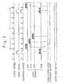
- the AC carrier signals from the carrier signal generating circuit 4 which are synchronized with the generation of the scanning output signals are used, so that the light emitting elements emit AC light beams as shown by CH1, CH2, ...CH8 of FIG. 3 towards the danger region.
- the scanning output signal occurring in the light transmission side scanning circuit 2 is normal so that a single signal is continuously generated along the time axis as shown in FIG. 3. Moreover if the outputs of the final stages of the light transmission side shift register 5 and the light reception side shift register 8 are synchronized, then the output of the scanning output signal checking circuit 9 and that of the coincidence detecting circuit 10 both become a logic value "1" so that the output of the AND gate 12 becomes a logic value "1". A detection output of a logic value of "1" indicating a safe condition is thus generated from the output amplifying circuit 14 via the sample/hold circuit 13, indicating a safe condition with no object in the danger region.
- the output of the sample/hold circuit 13 is held at a logic value "0", so that the output of the output amplifying circuit 14 also becomes a logic value "0", as shown by the dotted line in FIG. 3, indicating a dangerous condition with an object present in the danger region.
- the scanning output signal checking circuit 9 detects such abnormal conditions so that the output thereof becomes logic value "0". Also in the case wherein there is a discrepancy in the synchronization of the output of the final stage of the light transmission side shift register 5 and the light reception side shift register 8, the output of the coincidence detecting circuit 10 becomes a logic value "0". In either case, the output of the AND gate 12 becomes a logic value "0", so that a detection output indicating danger is generated from the output amplifying circuit 14.
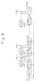
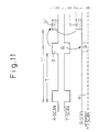
- FIG. 4 shows a circuit structure of the scanning output signal checking circuit 9.
- the scanning output signal checking circuit 9 comprises; an adding circuit 21 which incorporates a plurality of coupling capacitors C1 ⁇ C8 respectively connected in series to a plurality of input side resistors R1 ⁇ R8 through which a plurality of scanning output signals Fs1 ⁇ Fs8 (to be described later) are successively input from the light transmission side shift register 5 of the light transmission side scanning circuit 2; a plurality of diodes D21 ⁇ D28 acting as first diodes for clamping the respective output sides of the coupling capacitors C1 ⁇ C8 at the power source potential Vcc; and a plurality of diodes D11 ⁇ D18 acting as second diodes for rectifying/transmitting the outputs of the coupling capacitors C1 ⁇ C8 clamped at the power source potential Vcc by the diodes D21 ⁇ D28, to a single output terminal; and a fail-safe window comparator WC1 for threshold operation on the output level of the adding circuit 21.
- Scanning output signal Fs1, Fs2 .... Fs8 of the light transmission side shift register 5 are clamped at the power source potential Vcc by way of the respective capacitors C1 ⁇ C8 and resistors R1 ⁇ R8 using the respective diodes D21 ⁇ D28, and output from the diodes D11 ⁇ D18 to the window comparator WC1.
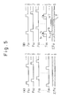
- the time chart of FIG. 5(A) shows the case where the scanning output signal of the light transmission side shift register 5 is normal.
- the time chart of FIG. 5(B) shows the abnormal case wherein the scanning output signal Fs8 of the light transmission side shift register 5 is not produced at the time that it should be output, and is erroneously produced at the generation time of the scanning output signal Fs1.
- the addition signal ⁇ Fsi of the adding circuit 21 is always at a logic level of logic value "1" (the output wherein the scanning output signals Fsi are superimposed on the power source potential Vcc of the window comparator).
- the addition signal ⁇ Fsi produces a logic level "b" of logic value "0" (the power source potential Vcc) since the scanning output signal Fs8 does not exist at a time t8 where the scanning output signal Fs8 should have been generated, and a logic level "a” of logic value "2" is produced since the scanning output signal Fs8 is superimposed on the scanning output signal Fs1 at a time t1 where the scanning output signal Fs1 only should be generated.
- the upper and lower limit threshold values of the window comparator WC1 as shown by HT and LT in FIG. 5(B) are set on either side of the logic level of logic value "1", being lower than logic value "2" and higher than logic value "0". Therefore, in the case of FIG. 5(A), a scanning output of logic value "1” indicating normal operation is generated from the window comparator WC1, while in the case of FIG. 5(B), since the addition signal ⁇ Fsi has logic levels of logic value "0" and "2", a scanning output of logic value "0" showing an abnormal condition is generated from the window comparator WC1.
- the circuit construction of the scanning output signal checking circuit 9 has the following features.
- the adding circuit 21 constituted by capacitors C1 ⁇ C8, diodes D11 ⁇ D18, and diodes D21 ⁇ D28 has capacitor coupling. Moreover, since it is clamped at the power source potential Vcc using the diodes D21 ⁇ D28 (coupling by a potential beyond the power source potential), then a signal is transmitted only when positive signal changes occur in the scanning output signals Fs1 ⁇ Fs8.
- the scanning output signal checking circuit 9 has another important fault checking function. Since the shift register is constituted by C-MOS IC, then when for example a disconnection fault occurs in the data input line to the light transmission side shift register 5, an erroneous output is produced, due for example to noise, in the flip-flop circuits of the shift register. In the case with the time chart of FIG. 5(A) wherein the output signals Fs1 ⁇ Fs8 of the shift register are output normally, the addition signal ⁇ Fsi is always at a logic level of "1". However when, as shown by the time chart of FIG.
- a scanning output signal Fs8 is also generated at a time t1 for generation of a scanning output signal Fs1 (normally the above error occurs at several different times), then at the time t1, the addition signal ⁇ Fsi becomes a logic level for two added scanning output signals.
- D-K flip-flops FF1 ⁇ FF8 constitute a shift register.
- a monostable multivibrator MM1 takes the scanning signals from the scanning signal generating circuit 1, extends these pulse width for a predetermined time, and outputs the extended signals to a data input terminal of a first stage flip-flop FF1 of the shift register.
- NOT circuits IV11 ⁇ IV81 are respectively connected to non inversion output terminals of the D - K flip-flops FF1 ⁇ FF8, with output sides thereof respectively connected to the cathode sides of light emitting elements LD1 ⁇ LD8.
- the anode sides of the light emitting elements LD1 ⁇ LD8 are respectively connected by way of current-limiting resistors R1 ⁇ R8, to the carrier signal generating circuit 4 which generates a carrier signal CRY of a predetermined frequency.
- input sides of NOT circuits IV12 ⁇ IV82 (second NOT circuits) are respectively connected to intermediate points between the respective light emitting elements LD1 ⁇ LD8 and the current-limiting resistors R1 ⁇ R8.
- the output sides of the NOT circuits IV12 ⁇ IV72 are respectively connected to data input terminals of the next stage flip-flops.
- IN is the scanning signal output from the scanning signal generating circuit 1.
- NOT circuit IV inverts the output of the last stage flip-flop FF8 for input to the coincidence detecting circuit 10.
- the signal resulting from pulse width extension of the scanning signal IN using the monostable multi-vibrator MM1 is used as the data side input signal for the first flip-flop FF1.
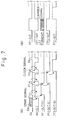
- FIG. 7(B) is a time chart showing the operation of the coupling circuits between the flip-flops. In this figure, the operation between flip-flops FF1 and FF2 is explained.
- the NOT circuit IV11 output becomes an L level, and the carrier signal CRY flows in the light emitting element LD1 so that an AC light beam is emitted.
- the input side of NOT circuit IV12 becomes L level and the output side becomes H level so that a signal of H level is input to the data input side of the next stage flip-flop FF2.
- the output of the flip-flop FF2 becomes H level. In this way, a construction is adopted wherein the scanning output signal Fs1 for input to the adding circuit 21 is generated as an input signal for the flip-flop FF2.
- the basic consideration concerning fault detection for the light transmission side scanning circuit of FIG. 6 which uses a shift register is based on the facts described below.
- the first is that when a fixed fault of logic value "0" (L level) occurs in the input signal to a flip-flop, then a logic value "1" (H level) does not occur in the output signal of the last stage flip-flop FF8.
- the second is that, when a fixed fault of logic value "1" occurs in the input signal to a flip-flop, (this situation includes the case wherein the light emitting element continuously emits light) the subsequent stage flip-flops are all fixed at a logic value "1".
- NOT circuits IV1 ⁇ IV8 (third NOT circuits) are connected to the inversion output terminal sides of respective flip-flops FF1 ⁇ FF8.
- Light receiving elements PD1 ⁇ PD8 are positioned to face the light emitting elements LD1 ⁇ LD8 with the danger region therebetween.
- the light beam received signals output from the light receiving elements PD1 ⁇ PD8 are amplified by fail-safe AC amplifying circuits A1 ⁇ A8 (refer to PCT-JP93/00411).
- the scanning signal IN is made a clock signal and the output signal of the monostable multivibrator MM2 based on the scanning input signal IN, is made the input signal for the data side of the first flip-flop FF1.
- output signals are generated by the flip-flops FF2 ⁇ FF8, sequentially and in synchronous with the generation of the clock signals.
- FIG. 9(B) shows the signal transmission process of the flip-flops FF1, FF2.
- the output of the flip-flop FF1 is at low level L (logic value "0")
- the output of the NOT circuit IV1 becomes a high level H (logic value "1")
- an AC output based on receipt of the light beam of the light receiving element PD1 is output as output signal Fr1.
- the connections of the lines "a", “b", “c” are made as shown in the figure.
- the circuit of FIG. 8 is constructed based on two forms of logic; the first being that, when a fault occurs in the AC amplifying circuits A1-A8, the light beam received output signals Fr1 ⁇ Fr8 are never output; and the second being that, when a fault occurs in the elements making up the shift register including the control lines "a", "b", then the influence of the fault is always apparent in the last stage flip-flop.
- the output of the last stage flip-flop FF8 from the light transmission side shift register 5 is inverted by the NOT circuit IV and is output as inversion output signal T-SCAN.
- the inverted output of the last stage flip-flop FF8 from the light reception side shift register 8 is inverted by the NOT circuit IV8 and is output as output signal R-SCAN of complementary relation to the inversion output signal T-SCAN of the light transmission side shift register 5.
- Both the inversion output signal T-SCAN and the output signal R-SCAN are added using the adding circuit 22, similar to that of FIG. 4, comprising capacitors C10, C20, diodes D10 ⁇ D40 and resistors R10, R20 (the resistors R10, R20 may be connected before the capacitors C10, C20).
- the addition output is then subjected to threshold operation in a fail-safe window comparator WC2.
- the output signal becomes a logic value "0" (indicating that the signals do not coincide).
- the fault mode of the coincidence detecting circuit 10 is similar to that shown in FIG. 4, in that, at the time of a circuit fault, the output of the addition signal X is stopped or becomes power source potential Vcc (in either case corresponding to logic value "0"), thus going outside of the threshold value range of the window comparator WC2, so that the output becomes a logic value "0".
- the construction of the sensor system can be simplified. Moreover, the addition operation to determine normal/abnormal operation of the generating conditions of the scanning output signal is simple and the capacitors can be ones with a small voltage endurance.
- the present invention can significantly improve the safety of an operator working in the common work space, and prevent injury of the operator by the machine, and thus has considerable industrial applicability.
Landscapes
- Physics & Mathematics (AREA)
- Life Sciences & Earth Sciences (AREA)
- General Life Sciences & Earth Sciences (AREA)
- General Physics & Mathematics (AREA)
- Geophysics (AREA)
- Electronic Switches (AREA)
- Geophysics And Detection Of Objects (AREA)
Abstract
Claims (6)
- Un capteur du type à faisceaux multi-axes et à sécurité intrinsèque. comprenant :caractérisé par :un circuit de balayage (2) du côté de l'émission de lumière pour le balayage séquentiel d'éléments d'émission de lumière :un circuit de balayage (6) du côté de la réception de la lumière pour le balayage séquentiel d'éléments de réception de lumière, de sorte que des faisceaux séquentiels soient produits à partir du côté de l'émission de la lumière vers le côté de la réception de la lumière pour la détection d'un objet dans une zone de danger ;un circuit à sécurité intrinsèque pour le redressement et le contrôle du niveau de signaux de sortie de balayage et pour la génération d'un signal présentant la valeur logique "1" dans le cas où les conditions de génération pour les signaux de sortie de balayage sont normales. la sortie passant à la valeur logique "0" dans le cas où les conditions de génération ne sont pas normales ;un circuit (1) de génération d'un signal de balayage pour générer un signal de balayage qui comprend un signal d'horloge à intervalle constant ;ledit circuit de balayage (2) du côté de l'émission de la lumière présentant un registre de décalage (5) pour la génération de signaux de sortie séquentiel pour chaque signal d'entrée du signal d'horloge originaire dudit circuit de génération de signal de balayage (1) pour générer un dit signal de sortie de balayage pour la commutation séquentielle et le pilotage de balayage d'une pluralité d'éléments d'émission de lumière (LD1-LD8) basés sur les signaux de sortie dudit registre à décalage (5 ) de sorte que des faisceaux lumineux séquentiels en courant alternatif soient émis par ladite pluralité d'éléments d'émission de lumière ;ledit circuit de balayage du côté de la réception de la lumière (6) présentant un registre à décalage pour la génération de signaux de sortie séquentiels pour chaque entrée du signal d'horloge. qui est dans le même que celui utilisé pour le circuit de balayage du côté de l'émission de la lumière. pour la génération d'un signal de sortie de balayage pour la commutation séquentielle et le pilotage du type à balayage d'un certain nombre d'éléments de réception de la lumière présents dans le même nombre que ladite pluralité d'éléments d'émission de la lumière et positionnés en face de ces derniers, sur la base du signal de sortie dudit registre à décalage. et pour générer un signal de sortie de réception de la lumière en courant alternatif quand un élément de réception de la lumière reçoit un faisceau lumineux à partir d'un élément d'émission de lumière :ledit circuit à sécurité intrinsèque comprenant un circuit d'amplification et de contrôle de niveau (11) pour amplifier un signal de sortie lumineux en courant alternatif reçu lorsqu'un tel signal est émis par ledit circuit de balayage du côté de la réception de la lumière, et pour ensuite contrôler le niveau et redresser le signal et émettre un signal de sortie de valeur logique "1", le signal de sortie passant à la valeur logique "0" lorsque le circuit d'amplification et de contrôle de niveau (11) est défaillant ;un circuit (9) de vérification du signal de sortie de balayage à sécurité intrinsèque pour additionner une pluralité de niveaux de signal de sortie de balayage dudit circuit de balayage du côté de l'émission de la lumière (2), et pour générer, dans le cas où le niveau logique de la valeur additionnée est "1", une sortie de valeur logique "1" pour une condition normale dans laquelle seul un signal de sortie de balayage est généré en continu, et pour générer, dans le cas où le niveau logique de ladite valeur d'addition est "2" ou plus, ou "0", un signal de sortie de valeur logique "0" pour au moins l'une desdites conditions anormales correspondant:au recouvrement d'un signal de sortie de balayage le long de l'axe temporel ; età l'absence de génération, pendant une seule période de balayage, d'au moins un signal de sortie de balayage, le signal de sortie prenant la valeur logique "0" dans le cas où le circuit de vérification du signal de sortie de balayage à sécurité intrinsèque est défaillant ;un circuit de détection de coïncidence (10) à sécurité intrinsèque pour réaliser une opération d'addition sur les signaux de sortie des derniers étages des registres à décalage respectifs (5,8) du côté de l'émission de lumière et du côté réception de la lumière et, dans le cas où le niveau logique de la valeur d'addition est "1", estimer que les sorties desdits derniers étages sont synchronisés et émettre un signal de sortie de valeur logique "1", et dans le cas où le niveau logique de la valeur d'addition est "2" ou "0". estimer que les signaux de sortie desdits derniers étages ne sont pas synchronisés et émettre un signal de sortie de valeur logique "0". lorsque le circuit de détection de coïncidence à sécurité intrinsèque est défaillant, un circuit ET à sécurité intrinsèque (12) pour effectuer une opération de produit logique sur les signaux de sortie respectifs de: ledit circuit d'amplification et de contrôle de niveau, ledit circuit de vérification du signal de sortie de balayage, et ledit circuit de détection de coïncidence et. dans le cas où tous les signaux de sortie sont d'une valeur logique "1", à générer un signal de sortie de valeur logique "1", le signal de sortie passant à une valeur logique "0" dans le cas où le circuit ET à sécurité intrinsèque (12) est défaillant, et un circuit échantillonneur/bloqueur à sécurité intrinsèque (13) pour bloquer le signal de sortie dudit circuit ET (12) quand sa valeur logique est "0", pendant au moins une période de balayage du signal de sortie de balayage. le signal de sortie passant à une valeur logique de "0" dans le cas où le circuit échantillonneur/bloqueur à sécurité intrinsèque (13) est défaillant.
- Un capteur du type à faisceaux lumineux multi-axes et à sécurité intrinsèque selon la revendication 1, dans lequel ledit circuit (2) de balayage du côté de l'émission de la lumière comprend :un registre à décalage (5) constitué d'une pluralité de bascules de type D-K (FF1-FF8) correspondant au nombre d'éléments d'émission de lumière, un multivibrateur monostable (MMI) qui reçoit les signaux de balayage à partir dudit circuit de génération de signaux de balayage (1) pour en élargir la largeur d'impulsion pendant une durée prédéterminée, et pour émettre en sortie les signaux élargis vers une borne d'entrée de données d'une bascule de premier étage (FF1) dudit registre à décalage, une pluralité de premiers circuits NON (IV77-IV781) reliés aux bornes de sortie non inverseuses des bascules respectives, une pluralité d'éléments d'émission de lumière (LD1-LD8) dont les côtés cathodes sont reliés aux bornes de sortie des circuits NON respectifs. un circuit de génération d'un signal porteur (4) pour générer un signal porteur présentant une fréquence prédéterminée. relié au côté anode des éléments respectifs d'émission de lumière via des résistances respectives (R1-R8), une pluralité de deuxièmes circuits NON (IV12-IV32) dont les côtés d'entrée sont reliés entre ledits éléments respectifs d'émission de lumière et des résistances, et dont les côtés sortie sont reliés à des bornes d'entrée de données des bascules respectives d'un étage suivant, et dans lequel le signal d'horloge du circuit de génération de signal de balayage (1) est fourni en entrée aux bornes d'entrée d'horloge desdites bascules respectives de type D-K. et les signaux de sortie vers ledit circuit de vérification du signal de sortie de balayage (1) étant prélevés à des points intermédiaires entre les deuxièmes circuits NON respectifs et les bornes respectives d'entrée de données des bascules.
- Un capteur du type à faisceaux lumineux multi-axes et à sécurité intrinsèque selon la revendication 1, dans lequel ledit circuit de balayage du côté de la réception de la lumière (6) comprend :
un registre à décalage (8) constitué d'une pluralité de bascules de type D-K correspondant au nombre d'éléments de réception de lumière (PD1-PD8), un multivibrateur monostable (MM2) pour recevoir les signaux de balayage à partir dudit circuit de génération de signaux de balayage (1) et pour en élargir la largeur des impulsions pendant une durée prédéterminée. et pour fournir en sortie les signaux élargis vers une borne d'entrée de données d'une bascule de premier étage dudit registre à décalage, une pluralité de troisièmes circuits NON (IV1-IV8) reliés à des bornes de sorties inverseuses des bascules respectives, une pluralité d'éléments de réception de la lumière (PD1-PD8) positionnés en face desdits éléments d'émission de lumière (LD1-LD8), une zone de danger étant située entre les deux, et une pluralité de circuits amplificateurs à courant alternatif (41-48) pour amplifier les signaux reçus correspondant aux faisceaux lumineux à partir desdits éléments respectifs de réception de la lumière, et dans lequel le même signal d'horloge que celui alimentant le circuit de balayage du côté de l'émission de la lumière (2) est fourni en entrée aux bornes d'entrée d'horloge desdites bascules respectives du type D-K, et les côtés sortie desdits troisièmes circuit NON étant reliés à des lignes de sortie respectives desdits circuits d'amplification en courant alternatif et ensuite reliés, via les lignes de sortie respectives, à des bornes d'entrée de donnée respectives de l'étage suivant de bascules. - Un capteur du type à faisceaux lumineux multi-axes et à sécurité intrinsèque selon la revendication 1, dans lequel ledit circuit de vérification des signaux de sortie de balayage (9) incorpore un circuit d'addition (21) comprenant une pluralité de condensateurs de couplage (C1-C8) reliés respectivement en série à une pluralité de bornes d'entrée pour l'entrée d'une pluralité de signaux de sortie de balayage, fournis séquentiellement en entrée partir du registre à décalage (5) du circuit de balayage du côté de l'émission de la lumière (2), une pluralité de premières diodes (D21-D28) pour limiter le niveau du côté de la sortie des condensateurs de couplage respectifs au niveau du potentiel de la source d'alimentation, et une pluralité de deuxièmes diodes (D11-D18) pour redresser/transmettre les signaux de sortie des condensateurs de couplage dont le niveau est limité au potentiel de la source d'alimentation grâce aux premières diodes respectives. vers une borne de sortie unique, et un premier comparateur à fenêtre à sécurité intrinsèque (WC1 ) qui réalise une opération de seuil sur le niveau de sortie dudit circuit d'addition. et émet un signal de sortie de valeur logique "1" dans le cas où le niveau de sortie est la valeur logique "1", en étant compris dans la gamme des valeurs de seuil, et émet un signal de sortie de valeur logique "0" dans le cas où le niveau de sortie est une valeur logique "0" ou "2" ou plus, en étant situé en dehors de la gamme des valeurs de seuil, le signal de sortie passant à une valeur logique de "0" dans le cas où le circuit de vérification du signal de sortie de balayage devient défaillant.
- Un capteur du type à faisceau lumineux multi-axes et à sécurité intrinsèque selon la revendication 1, dans lequel ledit circuit de détection de coïncidence (10 comprend :un circuit d'addition (22) comprenant une pluralité de condensateurs de couplage (C10, C20) reliés respectivement en série aux bornes d'entrée respectives et fournissant respectivement en entrée :le signal de sortie de la bascule de dernier étage du registre à décalage (5) dudit circuit de balayage du côté de l'émission de la lumière (2). et le signal de sortie de la bascule de dernier étage du registre à décalage (8) dudit circuit de balayage du côté de la réception de la lumière (6), des troisièmes diodes respectivement (D21-D28) pour limiter les niveaux du côté de la sortie des condensateurs de couplage respectifs au potentiel de la source d'alimentation. et des quatrièmes diodes respectives (D11-D18) pour le redressement et la transmission des signaux de sortie des condensateurs de couplage respectifs limitées au potentiel de la source d'alimentation par les troisièmes diodes respectives, à une borne de sortie unique, et un deuxième comparateur à fenêtre à sécurité intrinsèque (WC2) qui réalise une opération de seuil sur le niveau de sortie dudit circuit d'addition, et émet un signal de sortie de valeur logique "1" dans le cas où le niveau de sortie est une valeur logique "1" en étant compris dans la gamme des valeurs de seuil, et émet un signal de sortie de valeur logique de "0" quand le niveau de sortie est une valeur logique "0" ou "2" en se trouvant en dehors de la gamme des valeurs de seuil, le signal de sortie passant à une valeur logique "0" dans le cas où le circuit est défaillant, et dans lequel la sortie de la bascule de premier étage du registre à décalage (5) dudit circuit de balayage de côté de l'émission de la lumière (2) et le signal de sortie de la bascule de dernier étage du registre à décalage (8) dudit circuit de balayage du côté de la réception de la lumière (6), sont fournis en entrée selon une relation complémentaire l'un à l'autre, audit premier circuit d'addition (22).
- Un capteur du type à faisceaux lumineux multi-axes et à sécurité intrinsèque selon la revendication 1, dans lequel ledit circuit échantillonneur/bloqueur (13) comprend un circuit à retard d'activation à sécurité intrinsèque. fournissant un signal de sortie de valeur logique "0" au moment d'une défaillance.
Applications Claiming Priority (1)
| Application Number | Priority Date | Filing Date | Title |
|---|---|---|---|
| PCT/JP1993/001463 WO1995010789A1 (fr) | 1993-10-12 | 1993-10-12 | Capteur de faisceau lumineux a axes optiques multiples et surete integree |
Publications (3)
| Publication Number | Publication Date |
|---|---|
| EP0675376A1 EP0675376A1 (fr) | 1995-10-04 |
| EP0675376A4 EP0675376A4 (fr) | 1996-03-13 |
| EP0675376B1 true EP0675376B1 (fr) | 1998-01-07 |
Family
ID=14070573
Family Applications (1)
| Application Number | Title | Priority Date | Filing Date |
|---|---|---|---|
| EP93922066A Expired - Lifetime EP0675376B1 (fr) | 1993-10-12 | 1993-10-12 | Capteur de faisceau lumineux a axes optiques multiples et surete integree |
Country Status (5)
| Country | Link |
|---|---|
| US (1) | US5640006A (fr) |
| EP (1) | EP0675376B1 (fr) |
| JP (1) | JP3306715B2 (fr) |
| DE (1) | DE69316241T2 (fr) |
| WO (1) | WO1995010789A1 (fr) |
Cited By (1)
| Publication number | Priority date | Publication date | Assignee | Title |
|---|---|---|---|---|
| EP3483636A1 (fr) * | 2017-11-08 | 2019-05-15 | Leuze electronic GmbH + Co. KG | Rideau lumineux |
Families Citing this family (7)
| Publication number | Priority date | Publication date | Assignee | Title |
|---|---|---|---|---|
| EP0825458B1 (fr) | 1996-03-08 | 2002-10-30 | Nihon Shingo Kabushiki Kaisha | Barriere optique |
| EP0867274A1 (fr) * | 1996-09-03 | 1998-09-30 | The Nippon Signal Co. Ltd. | Appareil permettant d'agir automatiquement sur le fonctionnement du coulisseau d'une presse a securite integree |
| JPH1190696A (ja) | 1997-09-19 | 1999-04-06 | Nippon Signal Co Ltd:The | プレス機械の運転装置 |
| JP3986162B2 (ja) * | 1998-06-03 | 2007-10-03 | 株式会社キーエンス | 多重投光検出可能な多光軸光電スイッチ |
| JP5010835B2 (ja) * | 2006-02-24 | 2012-08-29 | パナソニック電工Sunx株式会社 | 多光軸光電センサ |
| CN106154303B (zh) * | 2016-06-20 | 2019-09-20 | 中国科学院高能物理研究所 | 信号处理装置以及时间探测装置 |
| EP4026973A1 (fr) * | 2021-01-07 | 2022-07-13 | CAME S.p.A. | Système de commande pour dispositifs de point d'accès |
Family Cites Families (12)
| Publication number | Priority date | Publication date | Assignee | Title |
|---|---|---|---|---|
| US4015122A (en) * | 1974-07-12 | 1977-03-29 | Rubinstein Walter M | Photo-electric object detection system |
| US4309693A (en) * | 1974-09-12 | 1982-01-05 | Analog Devices, Incorporated | Solid state digital to analog converter |
| JPS57142578A (en) * | 1981-02-28 | 1982-09-03 | Riken Lens Kogyo Kk | Automatic check device for light beam type safety device |
| JPH0669274B2 (ja) * | 1984-04-19 | 1994-08-31 | 日本信号株式会社 | 負荷駆動用スイッチ回路の監視装置 |
| JPS60227326A (ja) * | 1984-04-25 | 1985-11-12 | 日本信号株式会社 | 負荷駆動用スイツチ回路の監視装置 |
| JPS61198094A (ja) * | 1985-02-28 | 1986-09-02 | Fuji Electric Co Ltd | 光電スイツチ |
| JPS61198089A (ja) * | 1985-02-28 | 1986-09-02 | Hokuyo Automatic Co | 光電スイツチの検波回路 |
| JPH0625871Y2 (ja) * | 1989-08-01 | 1994-07-06 | 株式会社キーエンス | 光電スイッチ |
| JPH0470589A (ja) * | 1990-07-12 | 1992-03-05 | Koufu Nippon Denki Kk | フォトセンサ信号検出回路 |
| JPH0530068A (ja) * | 1991-07-24 | 1993-02-05 | Nec Corp | 調歩式データ多重化方式 |
| US5218196A (en) * | 1991-09-05 | 1993-06-08 | Frost Controls, Inc. | Light curtain system with system and watchdog microcontrollers |
| DE69318837T2 (de) * | 1993-03-31 | 1998-09-24 | Nippon Signal Co Ltd | Schaltung zur Überwachung der Drehung eines Motors sowie Vorrichtung mit einer solchen Schaltungzur Bestätigung des Anhaltens eines Motors |
-
1993
- 1993-10-12 EP EP93922066A patent/EP0675376B1/fr not_active Expired - Lifetime
- 1993-10-12 WO PCT/JP1993/001463 patent/WO1995010789A1/fr not_active Ceased
- 1993-10-12 US US08/454,378 patent/US5640006A/en not_active Expired - Fee Related
- 1993-10-12 JP JP51157595A patent/JP3306715B2/ja not_active Expired - Fee Related
- 1993-10-12 DE DE69316241T patent/DE69316241T2/de not_active Expired - Fee Related
Cited By (1)
| Publication number | Priority date | Publication date | Assignee | Title |
|---|---|---|---|---|
| EP3483636A1 (fr) * | 2017-11-08 | 2019-05-15 | Leuze electronic GmbH + Co. KG | Rideau lumineux |
Also Published As
| Publication number | Publication date |
|---|---|
| EP0675376A1 (fr) | 1995-10-04 |
| DE69316241T2 (de) | 1998-06-25 |
| US5640006A (en) | 1997-06-17 |
| EP0675376A4 (fr) | 1996-03-13 |
| DE69316241D1 (de) | 1998-02-12 |
| WO1995010789A1 (fr) | 1995-04-20 |
| JP3306715B2 (ja) | 2002-07-24 |
Similar Documents
| Publication | Publication Date | Title |
|---|---|---|
| EP0675376B1 (fr) | Capteur de faisceau lumineux a axes optiques multiples et surete integree | |
| EP0113478B1 (fr) | Système de sécurité en cas de défaillance pour des systèmes de transmission d'informations | |
| US7730782B2 (en) | Sensor device | |
| CN110685531B (zh) | 一种安全光幕 | |
| JPWO1995010789A1 (ja) | フェールセーフ多光軸光線式センサ | |
| US5130836A (en) | Optical transceiver | |
| US6858832B2 (en) | Photoelectric sensor having time changing means | |
| KR20190107560A (ko) | 광학식 안전 센서 | |
| EP0594852B1 (fr) | Circuit a balayage a surete intrinseque et capteur du type a faisceaux a axes optique multiples | |
| US6658030B1 (en) | Laser safety method and device for duplex open loop parallel optical link | |
| US11956010B2 (en) | Reduce link repair rate with added redundancy in parallel optical links | |
| JPH05149712A (ja) | 自動車の距離計測方法 | |
| JP2002204151A (ja) | 多光軸光電センサ | |
| JPH10224198A (ja) | 光電センサ | |
| JPH07208690A (ja) | 工作機の光線式安全装置 | |
| JPH01314991A (ja) | 光電スイッチ | |
| JPH0685717A (ja) | 平衡伝送路断線検出回路 | |
| JPH09199754A (ja) | 物体検知装置 | |
| JP5010835B2 (ja) | 多光軸光電センサ | |
| JP2729118B2 (ja) | 光学ラインセンサの診断方法 | |
| JPH0936725A (ja) | 光電センサ | |
| JPS59158140A (ja) | デ−タ伝送方式 | |
| SU1259268A1 (ru) | Устройство дл контрол дешифраторов | |
| JPH0936726A (ja) | 光エリアセンサ | |
| JPS61186041A (ja) | デ−タ通信方式 |
Legal Events
| Date | Code | Title | Description |
|---|---|---|---|
| PUAI | Public reference made under article 153(3) epc to a published international application that has entered the european phase |
Free format text: ORIGINAL CODE: 0009012 |
|
| 17P | Request for examination filed |
Effective date: 19950623 |
|
| AK | Designated contracting states |
Kind code of ref document: A1 Designated state(s): DE FR GB |
|
| A4 | Supplementary search report drawn up and despatched | ||
| AK | Designated contracting states |
Kind code of ref document: A4 Designated state(s): DE FR GB |
|
| 17Q | First examination report despatched |
Effective date: 19960924 |
|
| GRAG | Despatch of communication of intention to grant |
Free format text: ORIGINAL CODE: EPIDOS AGRA |
|
| GRAG | Despatch of communication of intention to grant |
Free format text: ORIGINAL CODE: EPIDOS AGRA |
|
| GRAH | Despatch of communication of intention to grant a patent |
Free format text: ORIGINAL CODE: EPIDOS IGRA |
|
| GRAH | Despatch of communication of intention to grant a patent |
Free format text: ORIGINAL CODE: EPIDOS IGRA |
|
| GRAA | (expected) grant |
Free format text: ORIGINAL CODE: 0009210 |
|
| AK | Designated contracting states |
Kind code of ref document: B1 Designated state(s): DE FR GB |
|
| REF | Corresponds to: |
Ref document number: 69316241 Country of ref document: DE Date of ref document: 19980212 |
|
| ET | Fr: translation filed | ||
| PLBE | No opposition filed within time limit |
Free format text: ORIGINAL CODE: 0009261 |
|
| STAA | Information on the status of an ep patent application or granted ep patent |
Free format text: STATUS: NO OPPOSITION FILED WITHIN TIME LIMIT |
|
| 26N | No opposition filed | ||
| REG | Reference to a national code |
Ref country code: GB Ref legal event code: IF02 |
|
| PGFP | Annual fee paid to national office [announced via postgrant information from national office to epo] |
Ref country code: GB Payment date: 20021004 Year of fee payment: 10 |
|
| PGFP | Annual fee paid to national office [announced via postgrant information from national office to epo] |
Ref country code: FR Payment date: 20021028 Year of fee payment: 10 |
|
| PGFP | Annual fee paid to national office [announced via postgrant information from national office to epo] |
Ref country code: DE Payment date: 20021029 Year of fee payment: 10 |
|
| PG25 | Lapsed in a contracting state [announced via postgrant information from national office to epo] |
Ref country code: GB Free format text: LAPSE BECAUSE OF NON-PAYMENT OF DUE FEES Effective date: 20031012 |
|
| PG25 | Lapsed in a contracting state [announced via postgrant information from national office to epo] |
Ref country code: DE Free format text: LAPSE BECAUSE OF NON-PAYMENT OF DUE FEES Effective date: 20040501 |
|
| GBPC | Gb: european patent ceased through non-payment of renewal fee |
Effective date: 20031012 |
|
| PG25 | Lapsed in a contracting state [announced via postgrant information from national office to epo] |
Ref country code: FR Free format text: LAPSE BECAUSE OF NON-PAYMENT OF DUE FEES Effective date: 20040630 |
|
| REG | Reference to a national code |
Ref country code: FR Ref legal event code: ST |