EP0675534A2 - Substrat SOI et procédé de fabrication du substrat - Google Patents
Substrat SOI et procédé de fabrication du substrat Download PDFInfo
- Publication number
- EP0675534A2 EP0675534A2 EP95103998A EP95103998A EP0675534A2 EP 0675534 A2 EP0675534 A2 EP 0675534A2 EP 95103998 A EP95103998 A EP 95103998A EP 95103998 A EP95103998 A EP 95103998A EP 0675534 A2 EP0675534 A2 EP 0675534A2
- Authority
- EP
- European Patent Office
- Prior art keywords
- oxide layer
- buried oxide
- substrate
- thickness
- oxidation
- Prior art date
- Legal status (The legal status is an assumption and is not a legal conclusion. Google has not performed a legal analysis and makes no representation as to the accuracy of the status listed.)
- Granted
Links
Images


Classifications
-
- H—ELECTRICITY
- H10—SEMICONDUCTOR DEVICES; ELECTRIC SOLID-STATE DEVICES NOT OTHERWISE PROVIDED FOR
- H10P—GENERIC PROCESSES OR APPARATUS FOR THE MANUFACTURE OR TREATMENT OF DEVICES COVERED BY CLASS H10
- H10P10/00—Bonding of wafers, substrates or parts of devices
-
- H—ELECTRICITY
- H10—SEMICONDUCTOR DEVICES; ELECTRIC SOLID-STATE DEVICES NOT OTHERWISE PROVIDED FOR
- H10P—GENERIC PROCESSES OR APPARATUS FOR THE MANUFACTURE OR TREATMENT OF DEVICES COVERED BY CLASS H10
- H10P30/00—Ion implantation into wafers, substrates or parts of devices
- H10P30/20—Ion implantation into wafers, substrates or parts of devices into semiconductor materials, e.g. for doping
- H10P30/208—Ion implantation into wafers, substrates or parts of devices into semiconductor materials, e.g. for doping of electrically inactive species
- H10P30/209—Ion implantation into wafers, substrates or parts of devices into semiconductor materials, e.g. for doping of electrically inactive species in silicon to make buried insulating layers
-
- H—ELECTRICITY
- H10—SEMICONDUCTOR DEVICES; ELECTRIC SOLID-STATE DEVICES NOT OTHERWISE PROVIDED FOR
- H10P—GENERIC PROCESSES OR APPARATUS FOR THE MANUFACTURE OR TREATMENT OF DEVICES COVERED BY CLASS H10
- H10P90/00—Preparation of wafers not covered by a single main group of this subclass, e.g. wafer reinforcement
- H10P90/19—Preparing inhomogeneous wafers
- H10P90/1904—Preparing vertically inhomogeneous wafers
- H10P90/1906—Preparing SOI wafers
- H10P90/1908—Preparing SOI wafers using silicon implanted buried insulating layers, e.g. oxide layers [SIMOX]
-
- H—ELECTRICITY
- H10—SEMICONDUCTOR DEVICES; ELECTRIC SOLID-STATE DEVICES NOT OTHERWISE PROVIDED FOR
- H10W—GENERIC PACKAGES, INTERCONNECTIONS, CONNECTORS OR OTHER CONSTRUCTIONAL DETAILS OF DEVICES COVERED BY CLASS H10
- H10W10/00—Isolation regions in semiconductor bodies between components of integrated devices
- H10W10/10—Isolation regions comprising dielectric materials
- H10W10/181—Semiconductor-on-insulator [SOI] isolation regions, e.g. buried oxide regions of SOI wafers
Definitions
- the present invention relates to an SOI substrate and a method of producing the SOI substrate having an insulation layer in a single crystal silicon substrate.
- the thin single crystal silicon layer provided on an insulation layer is preferable than making an integrated circuit on the bulky single crystal silicon substrate in view of the electrical characteristics of the elements and separation of the respective elements.
- a semiconductor substrate having, in an electrically insulated state, the surface single crystal silicon layer, in which the elements are formed, by making an insulation layer (SiO2) in the single crystal silicon substrate is generally called as "SOI (Silicon On Insulator)".
- SOI Silicon On Insulator
- the semiconductor substrate can be produced by a wafer bonding method or an oxygen-ion implantation method.
- the former wafer bonding method is that an oxide layer is formed on the single crystal silicon substrate, next an other single crystal silicon substrate is stuck to join thereon and a thin active silicon layer is formed by means of the whetted one of the single crystal silicon substrate.
- the later oxygen-ion implantation method is called as SIMOX (Separation by IMplanted OXygen) and has attracted attention lately to be preferable to form a thin-film active silicon layer to avail of a large-scale integratize, which forms a buried oxide layer inside of the silicon substrate by being allowed to react with Si and O in a high temperature anneal processing (1,100 - 1,200 °C) alter implanting a high-dose oxygen ion (16O + ) into the single crystal silicon substrate.
- a SIMOX substrate can cause the single crystal silicon substrate to be an active layer having an uniform thickness, though the surface single crystal silicon layer is not received with a processing of whet as a sticky substrate.
- the first object of the present invention to provide an SOI substrate which can increase a thickness of its buried oxide layer without increasing the dose of implanted oxygen ions to prevent an increase of crystal defect in a surface single-crystal silicon layer.
- the second object of the present invention is to provid a method of producing the SOI substrate capable of decreasing a pinhole density in the buried oxide layer.
- the third object of the present invention is to provide a method of producing the SOI substrate which improves the flatness of the buried oxide layer interface.
- the present invention is characterized to conduct an anneal processing after implanting the oxygen ions into the single crystal silicon substrate and additionally conduct an oxidation process to SIMOX substrate having the theoretical buried oxide layer thickness calculated from the dose of the implanted oxygen after annealing the implanted substrate in a high temperature atmosphere at within a range of over 1150 °C and less than a melting temperature of the silicon to increase the thickness of the buried oxide layer more than the theoretically obtained thickness by the anneal processing.
- the pinholes can be repaired by an additional treatment and the roughness of the interface is also flattened as expected.
- the SIMOX obtained after such additional high temperature oxidation treatment is of a qualified SOI substrate in which the buried oxide layer is thickened, there are few pinholes in the buried oxide layer, the flatness of the buried oxide layer interface is improved compared with those of the conventional SIMOX substrate.
- the present invention is materialized by detection of a phenomenon which the buried oxide layer grows in its layer when the high temperature oxidation treatment is practiced on the SIMOX substrate formed separately with the buried oxide layer by practicing the anneal processing after implanting the oxygen ions.
- the above-targeted SIMOX substrate is defined to include the thickness 320 nm of the surface active silicon layer and the thickness 89 nm of the buried oxide layer and is processed under the temperature set at 1350 °C and under an oxygen atmosphere controlled at a partial pressure (the same follow) of 70% O2 in an inert gas argon (Ar) and it is carried out the thus-oxidation treatment for four hours. As a result, it is recognized that the buried oxide layer grows into 118 nm.
- the buried oxide layer increased is sought out by controlling time in order to result in that the thickness of the thermally formed surface oxide layer is determined in about 400 nm (the oxidized thickness of the surface silicon layer is determined as 180 nm) under different oxidation temperatures changed by temperature conditions.
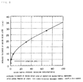
- increasing the oxidation temperature it is recognized that the thickness of the buried oxide layer is increased (the oxidation time: 77min. - 405min.).
- the effect of increasing the layer thickness is recognized over 1150 ° C. Accordingly, it can be understood that the increase rate of the buried oxide layer thickness is high level although the thickness of the surface oxide layer is the same and the buried oxide layer is thickly oxidized as the temperature is higher.
- Fig. 3 increasing the oxidation temperature, it is recognized that the thickness of the buried oxide layer is increased (the oxidation time: 77min. - 405min.).
- the effect of increasing the layer thickness is recognized over 1150 ° C. Accordingly, it can be understood that the increase rate of the buried oxide layer
- an oxidation temperature of the horizontal axis indicates a numerical value of 104 times a reciprocal number of a absolute temperature.
- Celsius temperature is indicated upper the drawings.
- the thickness of the buried oxide layer is increased as the oxidation temperature is higher.
- the buried oxide layer thickness can be increased upon an increase of oxidation temperature.
- the oxidation temperature is on or less than 1150 °C
- the increased thickness of the buried oxide layer is slight or when the oxidation time is for four hours as practical time, the increased thickness is less than a detecting level not to show an effect of increasing the thickness, but if the oxidation temperature will be increased at 1350 °C, an increase of the buried oxide layer thickness is about 30 nm.
- the buried oxide layer thickness of the conventional SIMOX is 80 - 90 nm, but in the present invention the buried oxide layer thickness reaches 100 - 110 nm when the oxidation treatment will be practiced at 1350 °C and the thickness o the surface oxide layer is 400 nm. It is therefore necessary to keep at least 1150 °C equal to the anneal processing temperature to attain a satisfactional increase of thickness.
- the maximum temperature should be lower than the melting temperature of the silicon, that is 1415 °C.
- the oxygen concentration in the oxygen atmosphere contributes to increase the thickness, so that when oxidizing at 1350 °C for four hours after the anneal processing and thereafter measuring the increase of the thickness of the buried oxide layer corresponding to a change of the oxygen partial pressure, a property chart as shown in Fig. 5 can be obtained.
- the thickness increase can be expected when the concentration of O2 is about over 1 %.
- the thickness increase is too slight to detect the increase because of the roughness of the buried oxide layer interface, so that the effect of increasing thickness of the buried oxide layer can be limitedly obtained when the oxygen concentration is over 1 %.
- the oxygen in the atmosphere is diffused from at least the surface silicon layer and the substrate silicon layer into the inside, so that the additional formation of SiO2 at the interface portion of the buried oxide layer can be generally regulated upon a temperature condition. It is therefore believed that the minimum concentration for diffusing to the silicon layer should be over 1 % as mentioned above. But, as can be understood from Fig. 5, the increase of the oxygen concentration at a certain high temperature can cause the increase of the thickness.
- the thickness of the surface silicon layer is required to be thinned depending upon final device condition, a so-called sacrifice oxidation treatment will be practiced.
- the sacrifice oxidation treatment is to form an oxide layer at a surface by heat oxidation and to remove the oxide layer from the surface by means of a generally known method to thin the surface silicon layer by a thickness of the oxidized silicon.
- the oxidation temperature should be set at a low temperature than the anneal temperature, more particularly at on or less than 1100 °C.
- the sacrifice oxidation may be practiced before or after the thickness increase process for the buried oxide layer.
- the producing method of the SOI substrate according to the present invention is characterized to have the steps of: implanting the oxygen ions into a single crystal silicon substrate; forming a buried oxide by an anneal process in which a high temperature process is practiced in an inert gas atmosphere; forming on the buried oxide layer a surface single-crystal silicon layer electrically insulating from the substrate by continuing the anneal process until the thickness of the buried oxide layer reaches a certain value theroretically calculated frim the dose of the implanted oxygen ions; and oxidizing the substrate in the high temperature oxidation atmosphere.
- the temperature of the high temperature oxidation process after the anneal process should be on or more than 1150 °C and less than a melting temperature of the single crystal silicon substrate and the high temperature oxidation process after the anneal process should be practiced in an oxygen gas atmosphere of which concentration is higher than that in the anneal process.
- the following steps can be further added that is to removing an oxide layer on surface of the substrate; practicing sacrifice oxidation at on or less that 1100 °C; and thinning the surface silicon layer by removing the sacrifice oxidation layer.
- the sacrifice oxidation is desirable to oxidize only the surface silicon layer but when oxidizing the SOI substrate over 1150 °C, the thickness of the buried oxide layer is naturally increased not to be able to control the thickness, so that it is required to be set below the high temperature oxidation condition temperature. Accordingly, in the sacrifice oxidation, the upper limit temperature of 1100 °C not to influence the buried oxide layer thickness is recommended.
- a property chart showing the relationship between the increase of the buried oxide layer thickness and the oxidation temperature will be obtained.
- the diameter and numbers of pinholes are changeable on an implantation condition of the oxygen ions and it is hard to directly understand the state of the pinhole, so that they should be obtained by a statistical way based on the ion implantation condition and the increased thickness of the buried oxide layer should be controlled to decrease a diameter of the main group pinholes.
- the thickness increase is one half, that is 25 nm, so that it should be based thereon.
- the rough interface condition can be developed by the ion implantation to thereby reduce the deviation of the electrical characteristics of devices.
- a property chart as shown in Fig. 6 can be obtained.
- the high temperature oxidation condition should be determined with reference to the property chart by which a necessary increase for flattening upon devices can be confirmed.
- the substrate implanted by the oxygen ions is set in a furnace and heated, and under a low oxygen concentration condition for preventing a generation of surface pits, the anneal processing will be carried out such that the thickness of the buried oxide layer becomes theoretical value calculated from the dose of the implanted oxygen.
- the thickness of the buried oxide layer can be increased by oxidizing the substrate having the buried oxide layer.
- the silicon substrate implanted by the oxygen ions is lead in the heat processing furnace in which the temperature is maintained at a range of 800 - 850 °C and the an inert gas are filled up not to generate crystal defects and is further heated until about 1100 - 1300 °C to obtain a stable state of its crystal.
- the gas atmosphere is controlled to include the oxygen by a concentration of 0.5 % in order to prevent generation of pits on the surface in the anneal processing.
- the gas atmosphere temperature reaches at or over the anneal temperature. It is therefore necessary to regulate the oxygen concentration to maintain the oxygen partial pressure of, for example, 70 % in the gas atmosphere, whereby the high temperature oxidation will be carried out at a constant temperature.
- the buried oxide layer in the substrate is that the oxide layer grows at the interface of the buried oxide layer of which the thickness depends upon the implanted oxygen ions, whereby the thickness of the buried oxide layer fromed becomes thicker than the theoretical value.
- the SOI substrate produced by the above-mentioned method is that the thickness of the buried oxide layer exceeds 90 nm, the dislocation density of the surface silicon single crystal layer is on or less than 100 cm2, the pinhole density of the buried oxide layer is on or less than 20 cm2, and the square root mean roughness of the buried oxide layer interface is on or less than 1 nm. Accordingly, the present invention is to provide the qualified SOI substrate in which the buried oxide layer is thickened, there are few pinholes in the buried oxide layer, the flatness of the buried oxide layer interface is improved compared with those of the conventional SIMOX substrate.
- the SIMOX substrate which was conventionally under the anneal processing after the oxygen ions are implanted is further oxidized in the high temperature atmosphere at a range from on or more than 1150 °C to less than the melting temperature of the silicon, whereby a thickness increase of the buried oxide layer can be attained on the prior buried oxide layer.
- the thickness increase of the layer can be attained by setting the oxygen concentration at over 1 % when oxidizing at a high temperature.
- the addtional oxide layer generated through the high temperature oxidation treatment can repair the pinholes or improve the flatness. If the sacrifice oxidation processing will be carried out before or after the high temperature oxidation treatment, the surface silicon single crystal layer can be thinned to the expected level.
- the high temperature oxidation treatment it can be separately conducted from the anneal processing against the substrate in which the buried oxide layer is formed in the prior anneal processing, but it will be also available to complete the anneal processing in the temperature increase process and to oxidize successively to increase the thickness of the buried oxide layer.
- the anneal processing will be practiced in the gas atmosphere containing therein the oxygen of low concentration while the temperature increases, and the oxidation treatment is practiced after the oxygen concentration is made strong to produce successively.
- Fig. 1 is an explanatory view showing successive processes for producing an SOI substrate in accordance with the present invention, the SOI substrate being depicted in section.
- the first process is of an oxygen-ion implantation process in which oxygen ions 16O + are implanted at a predetermined portion in depth in a single crystal silicon substrate 1 by means of an ion implanter.
- the dose of the implanted oxygen ions should be within 0.5 x 10¹⁸/cm2 to prevent a dislocation density of the surface silicon single crystal layer 2 from increasing and a strength of breakdown electric field across the buried oxide layer from decreasing.
- the reference numeral 3 in the drawings designates a layer of high-concentrated implantation of oxygen atmos.
- the second process is of a top coat forming process in which an anneal top coat 4 of SiO2 is formed on surface of the single crystal silicon substrate 1 by a CVD apparatus. But, it should not be understood that the anneal top coat is always necessary before the following third process.
- the third process is called an anneal process in which the substrate is processed under a furnace atmosphere containing therein Ar gas having 0.5% partial oxygen pressure, being maintained at 850 °C first and thereafter the temperature will be increased at 1350 °C.
- the above-explained anneal process is to stabilize the crystal state such that the layer of highly concentrated implantation of oxygen ions is transformed into a buried oxide layer 5.
- the reference numeral 6 should be understood to designate an oxide layer formed by the anneal process. As can be understood, the afore-described processes are the same with in the prior art.
- the fourth process it is an oxidization process at a high temperature and, more particularly the single crystal silicon substrate 1 is heated at on or more than 1150 °C and less than its melting temperature for several hours.
- the O2 gas concentration should be maintained in a range of over 1 % and on or less than 100 %.
- the drawings on the let side in Fig. 1 show a process to increase the buried oxide layer 5 formed through the anneal process by a thickness of additionally formed buried oxide layer 7.
- the reference numeral 8 designates an increased oxide layer after the high temperature oxidation process.
- FIG. 1 explain how the pin hole 9, made in the buried oxide layer owing to the masking effect when the oxygen ions were implanted into the single crystal silicon substrate 1 having thereon the particle, will be eliminated.
- the drawings shown in the right area in Fig. 1 explain an interface flattening process of the buried oxide layer, wherein a surface irregularity of the buried oxide layer 5 can be flattened or smoothed off by the additionally formed buried oxide layer 7.
- the improvement of flattening can be acknowledged from Fig. 6 of a property chart based on a relation of a square root mean roughness Rms to how the buried oxide layer is increased.
- the fourth process can be carried out after removing the oxide layer 6 formed through the third process.
- the fifth process is a sacrifice oxidation process of an oxidation treatment to make the surface single crystal silicon layer 2 become thinner.
- the sacrifice oxidation process may be carried out after removing the increased oxide layer 8. Otherwise, the sacrifice oxidation process may be done between the anneal process and the high temperature oxidation process. But, the sacrifice oxidation process can be conducted after removing the oxide layer 6.
- the third process of anneal processing can be carried out by simultaneously increasing the temperature and the high temperature oxidation is also available to be conducted after the temperature is increased.
- the substrate to be processed is preliminarily set in the furnace in which the anneal gas is filled up at a predetermined temperature to carry out the above-explained anneal process of the third process and when the furnace temperature exceeds 1200 °C, for example reaches at 1350 °C, the temperature is maintained.
- An additional oxygen is added into the thus-conditioned furnace to become an oxygen partial pressure of 70% and thereby the fourth high temperature oxidation process can be carried out. Examples of these processes are shown in Figs. 2(1) - 2(3). In Fig.
- the initial furnace temperature is within a range of 800 - 850 °C, and the furnace is filled up with the anneal gas and its temperature is increased to thereby obtain the buried oxide layer 5.
- the high temperature oxidation process is conducted independently after the anneal process.
- the high temperature oxidation process is carried out by increasing the oxygen partial pressure to be a predetermined oxygen concentration of 70 % in the furnace, increasing the temperature until 1350 °C and maintaining the temperature of 1350 °C.
- Fig. 2(2) it shows that the processes in Fig. 2(1) are successively carried out, in which the high temperature anneal processing is carried out, the oxygen partial pressure in the furnace is increased, and thereafter the high temperature oxidation process is practiced.
- Fig. 2(3) shows processes in which the anneal processing is practiced while the furnace temperature increases and the high temperature oxidation is thereafter carried out.
- the oxidation temperature may be set at 1300 °C.
- the examinations regarding the buried oxide layer thickness, pinhole density and flatness of the buried oxide layer interface are conducted for the buried oxide layer of the SIMOX substrate which is processed under the above-mentioned high temperature oxidation process after the anneal, which will be described as follows.
Landscapes
- Element Separation (AREA)
Applications Claiming Priority (3)
| Application Number | Priority Date | Filing Date | Title |
|---|---|---|---|
| JP7653894 | 1994-03-23 | ||
| JP76538/94 | 1994-03-23 | ||
| JP6076538A JP3036619B2 (ja) | 1994-03-23 | 1994-03-23 | Soi基板の製造方法およびsoi基板 |
Publications (3)
| Publication Number | Publication Date |
|---|---|
| EP0675534A2 true EP0675534A2 (fr) | 1995-10-04 |
| EP0675534A3 EP0675534A3 (fr) | 1996-11-13 |
| EP0675534B1 EP0675534B1 (fr) | 2000-03-01 |
Family
ID=13608053
Family Applications (1)
| Application Number | Title | Priority Date | Filing Date |
|---|---|---|---|
| EP95103998A Expired - Lifetime EP0675534B1 (fr) | 1994-03-23 | 1995-03-17 | Substrat SOI et procédé de fabrication du substrat |
Country Status (8)
| Country | Link |
|---|---|
| US (2) | US5658809A (fr) |
| EP (1) | EP0675534B1 (fr) |
| JP (1) | JP3036619B2 (fr) |
| KR (1) | KR0145824B1 (fr) |
| CZ (1) | CZ281798B6 (fr) |
| DE (1) | DE69515189T2 (fr) |
| FI (1) | FI951340A7 (fr) |
| TW (1) | TW401609B (fr) |
Cited By (10)
| Publication number | Priority date | Publication date | Assignee | Title |
|---|---|---|---|---|
| EP0704892A3 (fr) * | 1994-09-30 | 1996-11-13 | Nippon Steel Corp | Procédé pour produire un substrat semi-conducteur |
| EP0687002A3 (fr) * | 1994-06-03 | 1996-11-13 | Komatsu Denshi Kinzoku Kk | Procédé de fabrication d'un dispositif semi-conducteur du type SOI |
| EP0817248A3 (fr) * | 1996-07-05 | 1998-01-14 | Nippon Telegraph And Telephone Corporation | Méthode de fabrication d'un substrat SOI |
| EP0871216A1 (fr) * | 1997-04-11 | 1998-10-14 | SHARP Corporation | Procédé de fabrication de substrats SOI ayant un rendement élevé pour la récupération des dommages dus à une implantation ionique |
| WO2000016396A1 (fr) * | 1998-09-10 | 2000-03-23 | Nippon Steel Corporation | Substrat simox et procede de production associe |
| WO2001067510A1 (fr) * | 2000-03-10 | 2001-09-13 | Nippon Steel Corporation | Substrat simox et procede de production dudit substrat |
| US6403450B1 (en) * | 1998-04-07 | 2002-06-11 | Commissariat A L'energie Atomique | Heat treatment method for semiconductor substrates |
| WO2002080277A1 (fr) * | 2001-03-28 | 2002-10-10 | Nippon Steel Corporation | Processus de production de substrat simox et substrat simox |
| WO2004075298A1 (fr) | 2003-02-19 | 2004-09-02 | Shin-Etsu Handotai Co., Ltd. | Tranche soi et son procede de fabrication |
| FR2926925A1 (fr) * | 2008-01-29 | 2009-07-31 | Soitec Silicon On Insulator | Procede de fabrication d'heterostructures |
Families Citing this family (61)
| Publication number | Priority date | Publication date | Assignee | Title |
|---|---|---|---|---|
| JP3036619B2 (ja) * | 1994-03-23 | 2000-04-24 | コマツ電子金属株式会社 | Soi基板の製造方法およびsoi基板 |
| JPH10223551A (ja) * | 1997-02-12 | 1998-08-21 | Nec Corp | Soi基板の製造方法 |
| EP1037272A4 (fr) * | 1997-06-19 | 2004-07-28 | Asahi Chemical Ind | Substrat silicium sur isolant (soi) et procede d'elaboration, dispositif a semi-conducteurs et procede de fabrication |
| JPH1126390A (ja) * | 1997-07-07 | 1999-01-29 | Kobe Steel Ltd | 欠陥発生防止方法 |
| JPH1197377A (ja) * | 1997-09-24 | 1999-04-09 | Nec Corp | Soi基板の製造方法 |
| JPH11168106A (ja) * | 1997-09-30 | 1999-06-22 | Fujitsu Ltd | 半導体基板の処理方法 |
| KR100258096B1 (ko) * | 1997-12-01 | 2000-06-01 | 정선종 | 에스오아이(soi) 기판 제조방법 |
| EP1052687B1 (fr) * | 1998-02-02 | 2016-06-29 | Nippon Steel & Sumitomo Metal Corporation | Procede de fabrication d'un substrat soi. |
| US6117711A (en) * | 1998-03-02 | 2000-09-12 | Texas Instruments - Acer Incorporated | Method of making single-electron-tunneling CMOS transistors |
| JP3762144B2 (ja) | 1998-06-18 | 2006-04-05 | キヤノン株式会社 | Soi基板の作製方法 |
| KR100292818B1 (ko) * | 1998-07-02 | 2001-11-05 | 윤종용 | 모오스트랜지스터제조방법 |
| JP2000082679A (ja) * | 1998-07-08 | 2000-03-21 | Canon Inc | 半導体基板とその作製方法 |
| US6753229B1 (en) | 1998-12-04 | 2004-06-22 | The Regents Of The University Of California | Multiple-thickness gate oxide formed by oxygen implantation |
| JP3911901B2 (ja) | 1999-04-09 | 2007-05-09 | 信越半導体株式会社 | Soiウエーハおよびsoiウエーハの製造方法 |
| US6362075B1 (en) * | 1999-06-30 | 2002-03-26 | Harris Corporation | Method for making a diffused back-side layer on a bonded-wafer with a thick bond oxide |
| US6180487B1 (en) | 1999-10-25 | 2001-01-30 | Advanced Micro Devices, Inc. | Selective thinning of barrier oxide through masked SIMOX implant |
| EP1104936A1 (fr) | 1999-11-25 | 2001-06-06 | Mitsubishi Denki Kabushiki Kaisha | Procédé pour la fabrication d'un dispositif semi-conducteur et dispositif semi-conducteur fabriqué selon ce procédé |
| US6235607B1 (en) * | 1999-12-07 | 2001-05-22 | Advanced Micro Devices, Inc. | Method for establishing component isolation regions in SOI semiconductor device |
| US6476446B2 (en) | 2000-01-03 | 2002-11-05 | Advanced Micro Devices, Inc. | Heat removal by removal of buried oxide in isolation areas |
| US6613643B1 (en) | 2000-01-28 | 2003-09-02 | Advanced Micro Devices, Inc. | Structure, and a method of realizing, for efficient heat removal on SOI |
| US6486043B1 (en) | 2000-08-31 | 2002-11-26 | International Business Machines Corporation | Method of forming dislocation filter in merged SOI and non-SOI chips |
| JP4501263B2 (ja) * | 2000-09-20 | 2010-07-14 | 三菱マテリアル株式会社 | Soi基板の製造方法 |
| RU2193803C2 (ru) * | 2001-01-09 | 2002-11-27 | Институт микроэлектроники и информатики РАН | Способ ионного синтеза в кремнии захороненного слоя изолятора |
| US6414355B1 (en) | 2001-01-26 | 2002-07-02 | Advanced Micro Devices, Inc. | Silicon-on-insulator (SOI) chip having an active layer of non-uniform thickness |
| US6548369B1 (en) * | 2001-03-20 | 2003-04-15 | Advanced Micro Devices, Inc. | Multi-thickness silicon films on a single semiconductor-on-insulator (SOI) chip using simox |
| JP2002289552A (ja) | 2001-03-28 | 2002-10-04 | Nippon Steel Corp | Simox基板の製造方法およびsimox基板 |
| US6596570B2 (en) * | 2001-06-06 | 2003-07-22 | International Business Machines Corporation | SOI device with reduced junction capacitance |
| US20030230778A1 (en) | 2002-01-30 | 2003-12-18 | Sumitomo Mitsubishi Silicon Corporation | SOI structure having a SiGe Layer interposed between the silicon and the insulator |
| US7535100B2 (en) * | 2002-07-12 | 2009-05-19 | The United States Of America As Represented By The Secretary Of The Navy | Wafer bonding of thinned electronic materials and circuits to high performance substrates |
| TW577124B (en) * | 2002-12-03 | 2004-02-21 | Mosel Vitelic Inc | Method for estimating the forming thickness of the oxide layer and determining whether the pipes occur leakages |
| US6770495B1 (en) * | 2003-01-15 | 2004-08-03 | Advanced Micro Devices, Inc. | Method for revealing active regions in a SOI structure for DUT backside inspection |
| US7704318B2 (en) * | 2003-02-25 | 2010-04-27 | Sumco Corporation | Silicon wafer, SOI substrate, method for growing silicon single crystal, method for manufacturing silicon wafer, and method for manufacturing SOI substrate |
| US7112509B2 (en) * | 2003-05-09 | 2006-09-26 | Ibis Technology Corporation | Method of producing a high resistivity SIMOX silicon substrate |
| EP1695379B1 (fr) | 2003-12-16 | 2012-12-05 | International Business Machines Corporation | Procede de fabrication de couche isolante profilee de plaquettes de silicium sur isolant |
| JP2005229062A (ja) * | 2004-02-16 | 2005-08-25 | Canon Inc | Soi基板及びその製造方法 |
| JP2006032785A (ja) * | 2004-07-20 | 2006-02-02 | Sumco Corp | Soi基板の製造方法及びsoi基板 |
| US7358586B2 (en) * | 2004-09-28 | 2008-04-15 | International Business Machines Corporation | Silicon-on-insulator wafer having reentrant shape dielectric trenches |
| JP4609026B2 (ja) * | 2004-10-06 | 2011-01-12 | 信越半導体株式会社 | Soiウェーハの製造方法 |
| JP2006173568A (ja) | 2004-12-14 | 2006-06-29 | Korea Electronics Telecommun | Soi基板の製造方法 |
| US7211474B2 (en) * | 2005-01-18 | 2007-05-01 | International Business Machines Corporation | SOI device with body contact self-aligned to gate |
| US7071047B1 (en) | 2005-01-28 | 2006-07-04 | International Business Machines Corporation | Method of forming buried isolation regions in semiconductor substrates and semiconductor devices with buried isolation regions |
| US20060228492A1 (en) * | 2005-04-07 | 2006-10-12 | Sumco Corporation | Method for manufacturing SIMOX wafer |
| JP4876442B2 (ja) | 2005-06-13 | 2012-02-15 | 株式会社Sumco | Simoxウェーハの製造方法およびsimoxウェーハ |
| JP2007005563A (ja) | 2005-06-23 | 2007-01-11 | Sumco Corp | Simoxウェーハの製造方法 |
| KR100752182B1 (ko) * | 2005-10-12 | 2007-08-24 | 동부일렉트로닉스 주식회사 | 씨모스 이미지 센서 및 그 제조방법 |
| JP2007208023A (ja) | 2006-02-02 | 2007-08-16 | Sumco Corp | Simoxウェーハの製造方法 |
| JP2007227424A (ja) | 2006-02-21 | 2007-09-06 | Sumco Corp | Simoxウェーハの製造方法 |
| JP5157075B2 (ja) * | 2006-03-27 | 2013-03-06 | 株式会社Sumco | Simoxウェーハの製造方法 |
| JP5061489B2 (ja) | 2006-04-05 | 2012-10-31 | 株式会社Sumco | Simoxウェーハの製造方法 |
| JP2008244261A (ja) | 2007-03-28 | 2008-10-09 | Shin Etsu Handotai Co Ltd | Soi基板の製造方法 |
| US7955950B2 (en) * | 2007-10-18 | 2011-06-07 | International Business Machines Corporation | Semiconductor-on-insulator substrate with a diffusion barrier |
| KR100937599B1 (ko) * | 2007-12-17 | 2010-01-20 | 한국전자통신연구원 | 반도체 장치 및 그 형성 방법 |
| US7955909B2 (en) * | 2008-03-28 | 2011-06-07 | International Business Machines Corporation | Strained ultra-thin SOI transistor formed by replacement gate |
| US7998815B2 (en) * | 2008-08-15 | 2011-08-16 | Qualcomm Incorporated | Shallow trench isolation |
| KR100987794B1 (ko) | 2008-12-22 | 2010-10-13 | 한국전자통신연구원 | 반도체 장치의 제조 방법 |
| JP2009147383A (ja) * | 2009-03-26 | 2009-07-02 | Hitachi Kokusai Electric Inc | 熱処理方法 |
| JP5387451B2 (ja) * | 2010-03-04 | 2014-01-15 | 信越半導体株式会社 | Soiウェーハの設計方法及び製造方法 |
| JP2011176320A (ja) * | 2011-03-07 | 2011-09-08 | Hitachi Kokusai Electric Inc | 基板処理装置 |
| US9837334B2 (en) * | 2015-03-30 | 2017-12-05 | Globalfoundries Singapore Pte. Ltd. | Programmable active cooling device |
| FR3034565B1 (fr) * | 2015-03-30 | 2017-03-31 | Soitec Silicon On Insulator | Procede de fabrication d'une structure presentant une couche dielectrique enterree d'epaisseur uniforme |
| US11891821B2 (en) | 2021-10-14 | 2024-02-06 | John H. Kipp, Jr. | Mini-concrete trowel attachment assembly |
Family Cites Families (14)
| Publication number | Priority date | Publication date | Assignee | Title |
|---|---|---|---|---|
| US4749660A (en) * | 1986-11-26 | 1988-06-07 | American Telephone And Telegraph Company, At&T Bell Laboratories | Method of making an article comprising a buried SiO2 layer |
| FR2616590B1 (fr) * | 1987-06-15 | 1990-03-02 | Commissariat Energie Atomique | Procede de fabrication d'une couche d'isolant enterree dans un substrat semi-conducteur par implantation ionique et structure semi-conductrice comportant cette couche |
| KR910009318B1 (ko) * | 1987-09-08 | 1991-11-09 | 미쓰비시 뎅끼 가부시기가이샤 | 반도체 장치의 제조 및 고내압 파묻음 절연막 형성방법 |
| US4824698A (en) * | 1987-12-23 | 1989-04-25 | General Electric Company | High temperature annealing to improve SIMOX characteristics |
| JPH01239867A (ja) * | 1988-03-19 | 1989-09-25 | Fujitsu Ltd | 絶縁膜上半導体の形成方法 |
| US5116771A (en) * | 1989-03-20 | 1992-05-26 | Massachusetts Institute Of Technology | Thick contacts for ultra-thin silicon on insulator films |
| US5196355A (en) * | 1989-04-24 | 1993-03-23 | Ibis Technology Corporation | Simox materials through energy variation |
| JPH03240230A (ja) * | 1990-02-19 | 1991-10-25 | Fujitsu Ltd | 半導体装置の製造方法 |
| US5310689A (en) * | 1990-04-02 | 1994-05-10 | Motorola, Inc. | Method of forming a SIMOX structure |
| JP2607399B2 (ja) * | 1991-02-19 | 1997-05-07 | 日本電信電話株式会社 | 半導体基板の製造方法 |
| IT1255764B (it) * | 1992-05-15 | 1995-11-15 | Enichem | Struttura soi con ossido sottile e profondo ottenuta per impiantazioneionica ad alta energia e successivi trattamenti termici. |
| US5429955A (en) * | 1992-10-26 | 1995-07-04 | Texas Instruments Incorporated | Method for constructing semiconductor-on-insulator |
| JPH0794688A (ja) * | 1993-09-21 | 1995-04-07 | Nippon Telegr & Teleph Corp <Ntt> | Soi 基板の製造方法 |
| JP3036619B2 (ja) * | 1994-03-23 | 2000-04-24 | コマツ電子金属株式会社 | Soi基板の製造方法およびsoi基板 |
-
1994
- 1994-03-23 JP JP6076538A patent/JP3036619B2/ja not_active Expired - Lifetime
-
1995
- 1995-03-13 US US08/403,518 patent/US5658809A/en not_active Expired - Lifetime
- 1995-03-17 EP EP95103998A patent/EP0675534B1/fr not_active Expired - Lifetime
- 1995-03-17 DE DE69515189T patent/DE69515189T2/de not_active Expired - Lifetime
- 1995-03-20 KR KR1019950005872A patent/KR0145824B1/ko not_active Expired - Fee Related
- 1995-03-22 CZ CZ95726A patent/CZ281798B6/cs not_active IP Right Cessation
- 1995-03-22 FI FI951340A patent/FI951340A7/fi unknown
- 1995-06-16 TW TW084106175A patent/TW401609B/zh not_active IP Right Cessation
-
1997
- 1997-08-19 US US08/915,301 patent/US5918136A/en not_active Expired - Lifetime
Cited By (19)
| Publication number | Priority date | Publication date | Assignee | Title |
|---|---|---|---|---|
| EP0687002A3 (fr) * | 1994-06-03 | 1996-11-13 | Komatsu Denshi Kinzoku Kk | Procédé de fabrication d'un dispositif semi-conducteur du type SOI |
| US5665613A (en) * | 1994-06-03 | 1997-09-09 | Komatsu Electronic Metals Co., Ltd. | Method of making semiconductor device having SIMOX structure |
| EP0704892A3 (fr) * | 1994-09-30 | 1996-11-13 | Nippon Steel Corp | Procédé pour produire un substrat semi-conducteur |
| EP0817248A3 (fr) * | 1996-07-05 | 1998-01-14 | Nippon Telegraph And Telephone Corporation | Méthode de fabrication d'un substrat SOI |
| US5989981A (en) * | 1996-07-05 | 1999-11-23 | Nippon Telegraph And Telephone Corporation | Method of manufacturing SOI substrate |
| EP0871216A1 (fr) * | 1997-04-11 | 1998-10-14 | SHARP Corporation | Procédé de fabrication de substrats SOI ayant un rendement élevé pour la récupération des dommages dus à une implantation ionique |
| US6110845A (en) * | 1997-04-11 | 2000-08-29 | Sharp Kabushiki Kaisha | Process for fabricating SOI substrate with high-efficiency recovery from damage due to Ion implantation |
| US6403450B1 (en) * | 1998-04-07 | 2002-06-11 | Commissariat A L'energie Atomique | Heat treatment method for semiconductor substrates |
| WO2000016396A1 (fr) * | 1998-09-10 | 2000-03-23 | Nippon Steel Corporation | Substrat simox et procede de production associe |
| WO2001067510A1 (fr) * | 2000-03-10 | 2001-09-13 | Nippon Steel Corporation | Substrat simox et procede de production dudit substrat |
| US6767801B2 (en) | 2000-03-10 | 2004-07-27 | Nippon Steel Corporation | Simox substrate and method for production thereof |
| WO2002080277A1 (fr) * | 2001-03-28 | 2002-10-10 | Nippon Steel Corporation | Processus de production de substrat simox et substrat simox |
| US6740565B2 (en) | 2001-03-28 | 2004-05-25 | Nippon Steel Corporation | Process for fabrication of a SIMOX substrate |
| EP1298731A4 (fr) * | 2001-03-28 | 2008-04-09 | Nippon Steel Corp | Processus de production de substrat simox et substrat simox |
| WO2004075298A1 (fr) | 2003-02-19 | 2004-09-02 | Shin-Etsu Handotai Co., Ltd. | Tranche soi et son procede de fabrication |
| EP1596437A4 (fr) * | 2003-02-19 | 2009-12-02 | Shinetsu Handotai Kk | Tranche soi et son procede de fabrication |
| FR2926925A1 (fr) * | 2008-01-29 | 2009-07-31 | Soitec Silicon On Insulator | Procede de fabrication d'heterostructures |
| WO2009095380A1 (fr) * | 2008-01-29 | 2009-08-06 | S.O.I.Tec Silicon On Insulator Technologies | Procédé de fabrication d'hétérostructures |
| US8263475B2 (en) | 2008-01-29 | 2012-09-11 | Soitec | Method for manufacturing heterostructures |
Also Published As
| Publication number | Publication date |
|---|---|
| JP3036619B2 (ja) | 2000-04-24 |
| KR950027901A (ko) | 1995-10-18 |
| DE69515189D1 (de) | 2000-04-06 |
| FI951340A0 (fi) | 1995-03-22 |
| US5658809A (en) | 1997-08-19 |
| CZ281798B6 (cs) | 1997-02-12 |
| TW401609B (en) | 2000-08-11 |
| EP0675534B1 (fr) | 2000-03-01 |
| EP0675534A3 (fr) | 1996-11-13 |
| US5918136A (en) | 1999-06-29 |
| DE69515189T2 (de) | 2000-11-23 |
| CZ72695A3 (en) | 1995-11-15 |
| FI951340A7 (fi) | 1995-09-24 |
| KR0145824B1 (ko) | 1998-11-02 |
| JPH07263538A (ja) | 1995-10-13 |
Similar Documents
| Publication | Publication Date | Title |
|---|---|---|
| US5918136A (en) | SOI substrate and method of producing the same | |
| EP1279194B1 (fr) | Procede d'implantation utilisant des doses d'oxygene inferieures a la stoechiometrie a des energies differentes | |
| US6653209B1 (en) | Method of producing silicon thin film, method of constructing SOI substrate and semiconductor device | |
| EP1626440B1 (fr) | Plaquette SOI | |
| US6043166A (en) | Silicon-on-insulator substrates using low dose implantation | |
| EP0977255A2 (fr) | Procédé de fabricaiton d'un substrat SOI et substrat fabriqué par la dite méthode | |
| EP1596437A1 (fr) | Tranche soi et son procede de fabrication | |
| EP2413352A2 (fr) | Plaquette a silicium sur isolant et procédé de production de plaquette à silicium sur isolant | |
| JP4820801B2 (ja) | 貼り合わせウェーハの製造方法 | |
| US5665613A (en) | Method of making semiconductor device having SIMOX structure | |
| JP3204855B2 (ja) | 半導体基板の製造方法 | |
| EP0955670A2 (fr) | Procédé de fabrication d'une couche d'oxyde sur une couche SOI et procédé de fabrication d'une plaquette liée | |
| US6548379B1 (en) | SOI substrate and method for manufacturing the same | |
| JP2003309254A (ja) | 複数インプラント複数アニール・プロセスによる広いbox厚さ範囲にわたる中ドーズ量simox | |
| JP2007266059A (ja) | Simoxウェーハの製造方法 | |
| JP3995286B2 (ja) | Simox基板の製造方法 | |
| US20040187769A1 (en) | Method of producing SOI wafer | |
| US6037198A (en) | Method of fabricating SOI wafer | |
| EP1852908A1 (fr) | Processus d'implantation utilisant des doses d'oxygène, sous-stoechiométrique à énergies différentes | |
| Namavar et al. | On the Formation of Ultrathin Simox Structures by Low Energy Implantation1 | |
| EP1939927B1 (fr) | Procédé de production de plaquette collée | |
| JPH07321078A (ja) | 半導体ウェーハの製造方法 |
Legal Events
| Date | Code | Title | Description |
|---|---|---|---|
| PUAI | Public reference made under article 153(3) epc to a published international application that has entered the european phase |
Free format text: ORIGINAL CODE: 0009012 |
|
| 17P | Request for examination filed |
Effective date: 19950317 |
|
| AK | Designated contracting states |
Kind code of ref document: A2 Designated state(s): DE DK FR GB IT NL |
|
| RIN1 | Information on inventor provided before grant (corrected) |
Inventor name: KATAYAMA, TATSUHIKO, C/O KOMATSU ELECTRONIC METAL Inventor name: OHWADA, NORIHIKO, C/O NTT ELECTRONICS TECHNOLOGY Inventor name: IZUMI, KATSUTOSHI, C/O NIPPON TELEGRAPH AND Inventor name: NAKASHIMA, SADAO, C/O NIPPON TELEGRAPH AND |
|
| PUAL | Search report despatched |
Free format text: ORIGINAL CODE: 0009013 |
|
| AK | Designated contracting states |
Kind code of ref document: A3 Designated state(s): DE DK FR GB IT NL |
|
| 17Q | First examination report despatched |
Effective date: 19970205 |
|
| GRAG | Despatch of communication of intention to grant |
Free format text: ORIGINAL CODE: EPIDOS AGRA |
|
| GRAG | Despatch of communication of intention to grant |
Free format text: ORIGINAL CODE: EPIDOS AGRA |
|
| GRAH | Despatch of communication of intention to grant a patent |
Free format text: ORIGINAL CODE: EPIDOS IGRA |
|
| RAP1 | Party data changed (applicant data changed or rights of an application transferred) |
Owner name: NTT ELECTRONICS CORPORATION Owner name: NIPPON TELEGRAPH AND TELEPHONE CORPORATION Owner name: KOMATSU ELECTRONIC METALS CO., LTD |
|
| GRAH | Despatch of communication of intention to grant a patent |
Free format text: ORIGINAL CODE: EPIDOS IGRA |
|
| GRAA | (expected) grant |
Free format text: ORIGINAL CODE: 0009210 |
|
| AK | Designated contracting states |
Kind code of ref document: B1 Designated state(s): DE DK FR GB IT NL |
|
| PG25 | Lapsed in a contracting state [announced via postgrant information from national office to epo] |
Ref country code: NL Free format text: LAPSE BECAUSE OF FAILURE TO SUBMIT A TRANSLATION OF THE DESCRIPTION OR TO PAY THE FEE WITHIN THE PRESCRIBED TIME-LIMIT Effective date: 20000301 Ref country code: IT Free format text: LAPSE BECAUSE OF FAILURE TO SUBMIT A TRANSLATION OF THE DESCRIPTION OR TO PAY THE FEE WITHIN THE PRE;WARNING: LAPSES OF ITALIAN PATENTS WITH EFFECTIVE DATE BEFORE 2007 MAY HAVE OCCURRED AT ANY TIME BEFORE 2007. THE CORRECT EFFECTIVE DATE MAY BE DIFFERENT FROM THE ONE RECORDED.SCRIBED TIME-LIMIT Effective date: 20000301 |
|
| REF | Corresponds to: |
Ref document number: 69515189 Country of ref document: DE Date of ref document: 20000406 |
|
| PG25 | Lapsed in a contracting state [announced via postgrant information from national office to epo] |
Ref country code: GB Free format text: LAPSE BECAUSE OF NON-PAYMENT OF DUE FEES Effective date: 20000601 Ref country code: DK Free format text: LAPSE BECAUSE OF FAILURE TO SUBMIT A TRANSLATION OF THE DESCRIPTION OR TO PAY THE FEE WITHIN THE PRESCRIBED TIME-LIMIT Effective date: 20000601 |
|
| ET | Fr: translation filed | ||
| NLV1 | Nl: lapsed or annulled due to failure to fulfill the requirements of art. 29p and 29m of the patents act | ||
| PLBE | No opposition filed within time limit |
Free format text: ORIGINAL CODE: 0009261 |
|
| STAA | Information on the status of an ep patent application or granted ep patent |
Free format text: STATUS: NO OPPOSITION FILED WITHIN TIME LIMIT |
|
| GBPC | Gb: european patent ceased through non-payment of renewal fee |
Effective date: 20000601 |
|
| 26N | No opposition filed | ||
| REG | Reference to a national code |
Ref country code: FR Ref legal event code: CD Ref country code: FR Ref legal event code: CA |
|
| PGFP | Annual fee paid to national office [announced via postgrant information from national office to epo] |
Ref country code: FR Payment date: 20110401 Year of fee payment: 17 |
|
| PGFP | Annual fee paid to national office [announced via postgrant information from national office to epo] |
Ref country code: DE Payment date: 20110428 Year of fee payment: 17 |
|
| REG | Reference to a national code |
Ref country code: FR Ref legal event code: ST Effective date: 20121130 |
|
| REG | Reference to a national code |
Ref country code: DE Ref legal event code: R119 Ref document number: 69515189 Country of ref document: DE Effective date: 20121002 |
|
| PG25 | Lapsed in a contracting state [announced via postgrant information from national office to epo] |
Ref country code: FR Free format text: LAPSE BECAUSE OF NON-PAYMENT OF DUE FEES Effective date: 20120402 |
|
| PG25 | Lapsed in a contracting state [announced via postgrant information from national office to epo] |
Ref country code: DE Free format text: LAPSE BECAUSE OF NON-PAYMENT OF DUE FEES Effective date: 20121002 |