EP0676484A2 - Durchsichtige Diamantschichten und Verfahren zu ihrer Herstellung - Google Patents
Durchsichtige Diamantschichten und Verfahren zu ihrer Herstellung Download PDFInfo
- Publication number
- EP0676484A2 EP0676484A2 EP95201231A EP95201231A EP0676484A2 EP 0676484 A2 EP0676484 A2 EP 0676484A2 EP 95201231 A EP95201231 A EP 95201231A EP 95201231 A EP95201231 A EP 95201231A EP 0676484 A2 EP0676484 A2 EP 0676484A2
- Authority
- EP
- European Patent Office
- Prior art keywords
- diamond
- hydrogen
- diamond film
- film
- substrate
- Prior art date
- Legal status (The legal status is an assumption and is not a legal conclusion. Google has not performed a legal analysis and makes no representation as to the accuracy of the status listed.)
- Granted
Links
Images


Classifications
-
- C—CHEMISTRY; METALLURGY
- C23—COATING METALLIC MATERIAL; COATING MATERIAL WITH METALLIC MATERIAL; CHEMICAL SURFACE TREATMENT; DIFFUSION TREATMENT OF METALLIC MATERIAL; COATING BY VACUUM EVAPORATION, BY SPUTTERING, BY ION IMPLANTATION OR BY CHEMICAL VAPOUR DEPOSITION, IN GENERAL; INHIBITING CORROSION OF METALLIC MATERIAL OR INCRUSTATION IN GENERAL
- C23C—COATING METALLIC MATERIAL; COATING MATERIAL WITH METALLIC MATERIAL; SURFACE TREATMENT OF METALLIC MATERIAL BY DIFFUSION INTO THE SURFACE, BY CHEMICAL CONVERSION OR SUBSTITUTION; COATING BY VACUUM EVAPORATION, BY SPUTTERING, BY ION IMPLANTATION OR BY CHEMICAL VAPOUR DEPOSITION, IN GENERAL
- C23C16/00—Chemical coating by decomposition of gaseous compounds, without leaving reaction products of surface material in the coating, i.e. chemical vapour deposition [CVD] processes
- C23C16/22—Chemical coating by decomposition of gaseous compounds, without leaving reaction products of surface material in the coating, i.e. chemical vapour deposition [CVD] processes characterised by the deposition of inorganic material, other than metallic material
- C23C16/26—Deposition of carbon only
- C23C16/27—Diamond only
- C23C16/271—Diamond only using hot filaments
-
- C—CHEMISTRY; METALLURGY
- C01—INORGANIC CHEMISTRY
- C01B—NON-METALLIC ELEMENTS; COMPOUNDS THEREOF; METALLOIDS OR COMPOUNDS THEREOF NOT COVERED BY SUBCLASS C01C
- C01B32/00—Carbon; Compounds thereof
- C01B32/25—Diamond
-
- C—CHEMISTRY; METALLURGY
- C23—COATING METALLIC MATERIAL; COATING MATERIAL WITH METALLIC MATERIAL; CHEMICAL SURFACE TREATMENT; DIFFUSION TREATMENT OF METALLIC MATERIAL; COATING BY VACUUM EVAPORATION, BY SPUTTERING, BY ION IMPLANTATION OR BY CHEMICAL VAPOUR DEPOSITION, IN GENERAL; INHIBITING CORROSION OF METALLIC MATERIAL OR INCRUSTATION IN GENERAL
- C23C—COATING METALLIC MATERIAL; COATING MATERIAL WITH METALLIC MATERIAL; SURFACE TREATMENT OF METALLIC MATERIAL BY DIFFUSION INTO THE SURFACE, BY CHEMICAL CONVERSION OR SUBSTITUTION; COATING BY VACUUM EVAPORATION, BY SPUTTERING, BY ION IMPLANTATION OR BY CHEMICAL VAPOUR DEPOSITION, IN GENERAL
- C23C16/00—Chemical coating by decomposition of gaseous compounds, without leaving reaction products of surface material in the coating, i.e. chemical vapour deposition [CVD] processes
- C23C16/01—Chemical coating by decomposition of gaseous compounds, without leaving reaction products of surface material in the coating, i.e. chemical vapour deposition [CVD] processes on temporary substrates, e.g. substrates subsequently removed by etching
-
- C—CHEMISTRY; METALLURGY
- C23—COATING METALLIC MATERIAL; COATING MATERIAL WITH METALLIC MATERIAL; CHEMICAL SURFACE TREATMENT; DIFFUSION TREATMENT OF METALLIC MATERIAL; COATING BY VACUUM EVAPORATION, BY SPUTTERING, BY ION IMPLANTATION OR BY CHEMICAL VAPOUR DEPOSITION, IN GENERAL; INHIBITING CORROSION OF METALLIC MATERIAL OR INCRUSTATION IN GENERAL
- C23C—COATING METALLIC MATERIAL; COATING MATERIAL WITH METALLIC MATERIAL; SURFACE TREATMENT OF METALLIC MATERIAL BY DIFFUSION INTO THE SURFACE, BY CHEMICAL CONVERSION OR SUBSTITUTION; COATING BY VACUUM EVAPORATION, BY SPUTTERING, BY ION IMPLANTATION OR BY CHEMICAL VAPOUR DEPOSITION, IN GENERAL
- C23C16/00—Chemical coating by decomposition of gaseous compounds, without leaving reaction products of surface material in the coating, i.e. chemical vapour deposition [CVD] processes
- C23C16/22—Chemical coating by decomposition of gaseous compounds, without leaving reaction products of surface material in the coating, i.e. chemical vapour deposition [CVD] processes characterised by the deposition of inorganic material, other than metallic material
- C23C16/26—Deposition of carbon only
- C23C16/27—Diamond only
- C23C16/279—Diamond only control of diamond crystallography
-
- Y—GENERAL TAGGING OF NEW TECHNOLOGICAL DEVELOPMENTS; GENERAL TAGGING OF CROSS-SECTIONAL TECHNOLOGIES SPANNING OVER SEVERAL SECTIONS OF THE IPC; TECHNICAL SUBJECTS COVERED BY FORMER USPC CROSS-REFERENCE ART COLLECTIONS [XRACs] AND DIGESTS
- Y10—TECHNICAL SUBJECTS COVERED BY FORMER USPC
- Y10S—TECHNICAL SUBJECTS COVERED BY FORMER USPC CROSS-REFERENCE ART COLLECTIONS [XRACs] AND DIGESTS
- Y10S428/00—Stock material or miscellaneous articles
- Y10S428/922—Static electricity metal bleed-off metallic stock
- Y10S428/9335—Product by special process
- Y10S428/938—Vapor deposition or gas diffusion
Definitions
- the present invention relates to vapor deposited transparent polycrystalline diamond films. More particularly, the present invention relates the method of introducing a particular mixture of hydrogen and methane into a heated reaction zone adjacent to a substrate such as molybdenum, to effect polycrystalline diamond film deposition.
- thermoforming materials in the form of free-standing polycrystalline transparent diamond films having thicknesses of from 50 to 5000 microns with lateral dimensions exceeding 10 millimeters.
- the present invention is based on the discovery that vapor deposited transparent polycrystalline diamond film can be made at thicknesses greater than 50 microns by passing a particular hydrogen-methane mixture through a filament heated reaction zone adjacent to a suitable substrate, such as a molybdenum substrate, where the hydrogen-methane mixture introduced into the reaction zone has from about 1.5 to about 2 volume percent of methane, based on the total volume of hydrogen and methane.
- a transparent non-adherent polycrystalline diamond film having an optical absorbance of 2.1 cm ⁇ 1 to 32 cm ⁇ 1 can be formed at a growth rate of about 0.4 to 1.0 microns per hour. Thicknesses of at least 50 microns, and as high as 5000 microns or more, can be made having lateral dimensions exceeding 25 centimeters.
- a continuous free-standing, substantially transparent, polycrystalline diamond film having a thickness of at least 50 microns comprising (A) substantially vertical columnar diamond crystals having an average diameter of from about 20 to about 200 microns and a ⁇ 110 ⁇ orientation perpendicular to the base and up to 10,000 parts per million of chemically combined hydrogen which is sufficient to substantially saturate dangling carbon bonds at diamond crystal grain boundaries, carbon dislocations, and carbon vacancies and (B) diamond crystal grain boundaries separating the columnar diamond crystals of (A) where the diamond crystal grain boundaries have a 70°-90° orientation to the diamond crystal base.
- a method of growing a non-adherent substantially transparent polycrystalline diamond film on a substrate which comprises, passing a hydrogen-methane mixture through a heated reaction zone at a temperature of about 600° to about 1000°C and at a pressure from about 3 to about 24 torr which is sufficient to generate active carbon-hydrogen species in the heated reaction zone maintained at a distance of from about 0.3 to about 1 centimeter from the surface of the substrate, where the hydrogen-methane mixture introduced into the heated reaction zone has from 1.5 to about 2 volume percent of methane, based on the total volume of hydrogen and methane.
- Figure 1 shows a quartz bell jar having a metal flange which rests on a base. Inside the quartz bell jar, there is shown a support structure for a filament and several adjacent substrate sections.
- a quartz bell jar at 10 which can be 20"-30" tall and about 4"-6" wide having a metal collar at its base at 11 and a gas inlet at the top at 12.
- the metal collar portion rests on a rubber seal at 13 which can be Neoprene rubber.
- the rubber seal is supported by a metal base, such as steel base structure at 14 which has a vacuum opening at 15.
- the filament is secured by a screw at 21 to a metal plug at 22 which passes through a quartz insulating collar at 23 which is supported by an extension at 24. Electrical contacts are shown from the plug at 25 to a stud at 26 which is insulated from the metal base at 27.
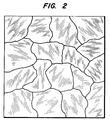
- Figure 2 showing a top view through an optical microscope of 10 to 200 micron columnar diamond crystals of the polycrystalline diamond film of the present invention separated by atomic grain boundaries such as shown at 30.
- FIG. 3 and Figure 3A A further reference to the polycrystalline diamond film of the present invention is shown by Figure 3 and Figure 3A.
- a side view of the polycrystalline diamond film in cross Section, and a detail at 3A further illustrates the substantially transparent columns of diamond crystals having a ⁇ 110 ⁇ orientation perpendicular to the base. Grain boundaries between adjacent diamond crystals having hydrogen atoms saturating dangling carbon bonds are shown at 40 and in detail at 41, where at least 50% of the carbon atoms are believed to be tetrahedrally bonded based on Raman spectroscopy, infrared and X-ray analysis.
- the above mechanism is one possible explanation as to how the transparent diamond film grows on the substrate.
- polycrystalline diamond films made in accordance with the practice of the present invention can be used in a variety of glazing applications as well as heat sinks or semiconductors.
- the tungsten filament was maintained at a temperature between about 2020 to 2040 .
- a separation of about 7-8 millimeters was maintained between the filament and the molybdenum substrate during the deposition which lasted approximately 30 days.
- the substrate temperature was estimated at about 800 . C during the deposition period.
- Transparent polycrystalline diamond films having thicknesses of about 500 microns and lateral dimensions equivalent to the substrates separated from the substrate during the cooling period.
- the diamond films were found to be of good crystalline quality as shown by Raman spectra having an intense peak at 1332 cm ⁇ 1.
- the diamond films were also found to have the characteristic two phonon adsorption of material diamond in the range of 1600-2650 cm ⁇ 1 by infrared spectroscopy.
Landscapes
- Chemical & Material Sciences (AREA)
- Organic Chemistry (AREA)
- Metallurgy (AREA)
- Engineering & Computer Science (AREA)
- Mechanical Engineering (AREA)
- Materials Engineering (AREA)
- General Chemical & Material Sciences (AREA)
- Chemical Kinetics & Catalysis (AREA)
- Inorganic Chemistry (AREA)
- Crystallography & Structural Chemistry (AREA)
- Geology (AREA)
- General Life Sciences & Earth Sciences (AREA)
- Life Sciences & Earth Sciences (AREA)
- Crystals, And After-Treatments Of Crystals (AREA)
- Carbon And Carbon Compounds (AREA)
- Chemical Vapour Deposition (AREA)
- Preparing Plates And Mask In Photomechanical Process (AREA)
Applications Claiming Priority (3)
| Application Number | Priority Date | Filing Date | Title |
|---|---|---|---|
| US07/407,179 US5110579A (en) | 1989-09-14 | 1989-09-14 | Transparent diamond films and method for making |
| US407179 | 1989-09-14 | ||
| EP90116058A EP0417512B1 (de) | 1989-09-14 | 1990-08-22 | Durchsichtige Diamantschichten und Verfahren zu ihrer Herstellung |
Related Parent Applications (1)
| Application Number | Title | Priority Date | Filing Date |
|---|---|---|---|
| EP90116058A Division EP0417512B1 (de) | 1989-09-14 | 1990-08-22 | Durchsichtige Diamantschichten und Verfahren zu ihrer Herstellung |
Publications (3)
| Publication Number | Publication Date |
|---|---|
| EP0676484A2 true EP0676484A2 (de) | 1995-10-11 |
| EP0676484A3 EP0676484A3 (de) | 1995-12-06 |
| EP0676484B1 EP0676484B1 (de) | 1999-03-24 |
Family
ID=23610962
Family Applications (2)
| Application Number | Title | Priority Date | Filing Date |
|---|---|---|---|
| EP95201231A Revoked EP0676484B1 (de) | 1989-09-14 | 1990-08-22 | Durchsichtige Diamantschichten und Verfahren zu ihrer Herstellung |
| EP90116058A Revoked EP0417512B1 (de) | 1989-09-14 | 1990-08-22 | Durchsichtige Diamantschichten und Verfahren zu ihrer Herstellung |
Family Applications After (1)
| Application Number | Title | Priority Date | Filing Date |
|---|---|---|---|
| EP90116058A Revoked EP0417512B1 (de) | 1989-09-14 | 1990-08-22 | Durchsichtige Diamantschichten und Verfahren zu ihrer Herstellung |
Country Status (8)
| Country | Link |
|---|---|
| US (1) | US5110579A (de) |
| EP (2) | EP0676484B1 (de) |
| JP (2) | JP3176614B2 (de) |
| KR (2) | KR970005187B1 (de) |
| AT (2) | ATE178102T1 (de) |
| CA (1) | CA2021113A1 (de) |
| DE (2) | DE69023847T2 (de) |
| IE (1) | IE73671B1 (de) |
Cited By (3)
| Publication number | Priority date | Publication date | Assignee | Title |
|---|---|---|---|---|
| WO1999001589A1 (en) * | 1997-07-01 | 1999-01-14 | E.I. Du Pont De Nemours And Company | Colorless diamond-like carbon coatings |
| GB2397826A (en) * | 2002-12-18 | 2004-08-04 | Bosch Gmbh Robert | Tribologically stressed structural element coated with diamond-like carbon and gas engine or internal combustion engine provided therewith |
| US8114505B2 (en) | 2003-12-05 | 2012-02-14 | Morgan Advanced Ceramics, Inc. | Free-standing silicon carbide articles formed by chemical vapor deposition and methods for their manufacture |
Families Citing this family (38)
| Publication number | Priority date | Publication date | Assignee | Title |
|---|---|---|---|---|
| US6413589B1 (en) | 1988-11-29 | 2002-07-02 | Chou H. Li | Ceramic coating method |
| US5273731A (en) * | 1989-09-14 | 1993-12-28 | General Electric Company | Substantially transparent free standing diamond films |
| KR930011413B1 (ko) | 1990-09-25 | 1993-12-06 | 가부시키가이샤 한도오따이 에네루기 겐큐쇼 | 펄스형 전자파를 사용한 플라즈마 cvd 법 |
| US5902640A (en) * | 1991-11-25 | 1999-05-11 | The University Of Chicago | Method of improving field emission characteristics of diamond thin films |
| US5286524A (en) * | 1991-12-13 | 1994-02-15 | General Electric Company | Method for producing CVD diamond film substantially free of thermal stress-induced cracks |
| US5443032A (en) * | 1992-06-08 | 1995-08-22 | Air Products And Chemicals, Inc. | Method for the manufacture of large single crystals |
| GB9214479D0 (en) * | 1992-07-08 | 1992-08-19 | Atomic Energy Authority Uk | Pressure transducers |
| US5377522A (en) * | 1993-10-27 | 1995-01-03 | General Electric Company | Diamond wire die with positioned opening |
| US5361621A (en) * | 1993-10-27 | 1994-11-08 | General Electric Company | Multiple grained diamond wire die |
| US5465603A (en) * | 1993-11-05 | 1995-11-14 | General Electric Company | Optically improved diamond wire die |
| US5514242A (en) * | 1993-12-30 | 1996-05-07 | Saint Gobain/Norton Industrial Ceramics Corporation | Method of forming a heat-sinked electronic component |
| EP0668372A1 (de) * | 1994-02-16 | 1995-08-23 | General Electric Company | Halbtransparenter Diamantfilm |
| EP0668371A1 (de) * | 1994-02-16 | 1995-08-23 | General Electric Company | Halbtransparanter Diamantfilm |
| EP0678592A1 (de) * | 1994-04-20 | 1995-10-25 | General Electric Company | Verbesserter CVD-Diamant |
| US5507987A (en) * | 1994-04-28 | 1996-04-16 | Saint Gobain/Norton Industrial Ceramics Corp. | Method of making a free-standing diamond film with reduced bowing |
| US5811631A (en) * | 1994-04-29 | 1998-09-22 | Motorola, Inc. | Apparatus and method for decomposition of chemical compounds using a self-supporting member |
| US5451430A (en) * | 1994-05-05 | 1995-09-19 | General Electric Company | Method for enhancing the toughness of CVD diamond |
| US5672395A (en) * | 1994-05-05 | 1997-09-30 | General Electric Company | Method for enhancing the toughness of CVD diamond |
| US5551277A (en) * | 1994-09-23 | 1996-09-03 | General Electric Company | Annular diamond bodies |
| US5634370A (en) * | 1995-07-07 | 1997-06-03 | General Electric Company | Composite diamond wire die |
| US5636545A (en) * | 1995-07-07 | 1997-06-10 | General Electric Company | Composite diamond wire die |
| US5634369A (en) * | 1995-07-07 | 1997-06-03 | General Electric Company | Composite diamond wire die |
| US5620745A (en) * | 1995-12-19 | 1997-04-15 | Saint Gobain/Norton Industrial Ceramics Corp. | Method for coating a substrate with diamond film |
| US6143412A (en) * | 1997-02-10 | 2000-11-07 | President And Fellows Of Harvard College | Fabrication of carbon microstructures |
| US5937514A (en) | 1997-02-25 | 1999-08-17 | Li; Chou H. | Method of making a heat-resistant system |
| US6286206B1 (en) | 1997-02-25 | 2001-09-11 | Chou H. Li | Heat-resistant electronic systems and circuit boards |
| US6582513B1 (en) * | 1998-05-15 | 2003-06-24 | Apollo Diamond, Inc. | System and method for producing synthetic diamond |
| US6858080B2 (en) * | 1998-05-15 | 2005-02-22 | Apollo Diamond, Inc. | Tunable CVD diamond structures |
| US8591856B2 (en) * | 1998-05-15 | 2013-11-26 | SCIO Diamond Technology Corporation | Single crystal diamond electrochemical electrode |
| US6458017B1 (en) | 1998-12-15 | 2002-10-01 | Chou H. Li | Planarizing method |
| US6676492B2 (en) | 1998-12-15 | 2004-01-13 | Chou H. Li | Chemical mechanical polishing |
| US6976904B2 (en) * | 1998-07-09 | 2005-12-20 | Li Family Holdings, Ltd. | Chemical mechanical polishing slurry |
| AU2001281404B2 (en) | 2001-08-08 | 2008-07-03 | Apollo Diamond, Inc. | System and method for producing synthetic diamond |
| US20050123713A1 (en) | 2003-12-05 | 2005-06-09 | Forrest David T. | Articles formed by chemical vapor deposition and methods for their manufacture |
| US7469569B2 (en) * | 2003-12-10 | 2008-12-30 | Diamond Innovations, Inc. | Wire drawing die and method of making |
| WO2005080645A2 (en) * | 2004-02-13 | 2005-09-01 | Apollo Diamond, Inc. | Diamond structure separation |
| JP6133647B2 (ja) * | 2013-03-25 | 2017-05-24 | シチズン時計株式会社 | 方位計測機能付き電子機器 |
| CN117202064B (zh) * | 2023-09-22 | 2024-05-10 | 郑州大学 | 基于金刚石微悬臂梁的光学传声器及传声系统 |
Family Cites Families (21)
| Publication number | Priority date | Publication date | Assignee | Title |
|---|---|---|---|---|
| US3030187A (en) * | 1958-07-23 | 1962-04-17 | Union Carbide Corp | Synthesis of diamond |
| US3630679A (en) * | 1968-06-26 | 1971-12-28 | Univ Case Western Reserve | Diamond growth process |
| JPS5927754B2 (ja) * | 1981-12-17 | 1984-07-07 | 科学技術庁無機材質研究所長 | ダイヤモンドの合成法 |
| JPS58135117A (ja) * | 1982-01-29 | 1983-08-11 | Natl Inst For Res In Inorg Mater | ダイヤモンドの製造法 |
| JPS5918197A (ja) * | 1982-07-19 | 1984-01-30 | Sumitomo Electric Ind Ltd | ダイヤモンドの気相合成法 |
| JPS60112699A (ja) * | 1983-11-24 | 1985-06-19 | Nec Corp | ダイヤモンドの製造方法 |
| JPS60118694A (ja) * | 1983-11-29 | 1985-06-26 | Mitsubishi Metal Corp | ダイヤモンドの低圧合成法 |
| JPS60127292A (ja) * | 1983-12-15 | 1985-07-06 | Asahi Chem Ind Co Ltd | ダイヤモンドの製造法 |
| JPS60141697A (ja) * | 1983-12-27 | 1985-07-26 | Pioneer Electronic Corp | ダイヤモンド振動板の製造方法 |
| JPS60186500A (ja) * | 1984-03-06 | 1985-09-21 | Nec Corp | 気相からのダイヤモンド合成法 |
| DE3690606C2 (de) * | 1985-11-25 | 1995-09-21 | Yoichi Hirose | Verfahren zur Synthese von Diamant |
| US4900628A (en) * | 1986-07-23 | 1990-02-13 | Sumitomo Electric Industries, Ltd. | Gaseous phase synthesized diamond and method for synthesizing same |
| JPS63107898A (ja) * | 1986-10-23 | 1988-05-12 | Natl Inst For Res In Inorg Mater | プラズマを用いるダイヤモンドの合成法 |
| JPS63153815A (ja) * | 1986-12-17 | 1988-06-27 | Fujitsu Ltd | ダイヤモンドの気相合成方法 |
| JPS63201601A (ja) * | 1987-02-18 | 1988-08-19 | Res Dev Corp Of Japan | 光学用窓材及びその製造方法 |
| EP0286306B1 (de) * | 1987-04-03 | 1993-10-06 | Fujitsu Limited | Verfahren und Vorrichtung zur Gasphasenabscheidung von Diamant |
| JP2603257B2 (ja) * | 1987-06-05 | 1997-04-23 | 株式会社神戸製鋼所 | ダイヤモンド多層薄膜 |
| US4830702A (en) * | 1987-07-02 | 1989-05-16 | General Electric Company | Hollow cathode plasma assisted apparatus and method of diamond synthesis |
| US4925701A (en) * | 1988-05-27 | 1990-05-15 | Xerox Corporation | Processes for the preparation of polycrystalline diamond films |
| US4958592A (en) * | 1988-08-22 | 1990-09-25 | General Electric Company | Resistance heater for diamond production by CVD |
| US4970986A (en) * | 1989-08-03 | 1990-11-20 | General Electric Company | Apparatus for synthetic diamond deposition including spring-tensioned filaments |
-
1989
- 1989-09-14 US US07/407,179 patent/US5110579A/en not_active Expired - Lifetime
-
1990
- 1990-07-12 CA CA002021113A patent/CA2021113A1/en not_active Abandoned
- 1990-07-13 IE IE256190A patent/IE73671B1/en not_active IP Right Cessation
- 1990-08-22 DE DE69023847T patent/DE69023847T2/de not_active Revoked
- 1990-08-22 AT AT95201231T patent/ATE178102T1/de active
- 1990-08-22 EP EP95201231A patent/EP0676484B1/de not_active Revoked
- 1990-08-22 EP EP90116058A patent/EP0417512B1/de not_active Revoked
- 1990-08-22 DE DE69033022T patent/DE69033022T2/de not_active Revoked
- 1990-08-22 AT AT90116058T patent/ATE130876T1/de not_active IP Right Cessation
- 1990-09-11 JP JP23916090A patent/JP3176614B2/ja not_active Expired - Lifetime
- 1990-09-13 KR KR1019900014427A patent/KR970005187B1/ko not_active Expired - Fee Related
-
1997
- 1997-02-12 KR KR97004067A patent/KR0134248B1/ko not_active Expired - Lifetime
- 1997-07-01 JP JP9175070A patent/JPH1067596A/ja active Pending
Cited By (5)
| Publication number | Priority date | Publication date | Assignee | Title |
|---|---|---|---|---|
| WO1999001589A1 (en) * | 1997-07-01 | 1999-01-14 | E.I. Du Pont De Nemours And Company | Colorless diamond-like carbon coatings |
| GB2397826A (en) * | 2002-12-18 | 2004-08-04 | Bosch Gmbh Robert | Tribologically stressed structural element coated with diamond-like carbon and gas engine or internal combustion engine provided therewith |
| GB2397826B (en) * | 2002-12-18 | 2005-07-27 | Bosch Gmbh Robert | Tribologically stressed structural element and gas engine or internal combustion engine therewith |
| US7455906B2 (en) | 2002-12-18 | 2008-11-25 | Robert Bosch Gmbh | Tribologically loaded component and accompanying gas engine or internal combustion engine |
| US8114505B2 (en) | 2003-12-05 | 2012-02-14 | Morgan Advanced Ceramics, Inc. | Free-standing silicon carbide articles formed by chemical vapor deposition and methods for their manufacture |
Also Published As
| Publication number | Publication date |
|---|---|
| ATE178102T1 (de) | 1999-04-15 |
| EP0417512B1 (de) | 1995-11-29 |
| DE69023847T2 (de) | 1996-05-30 |
| US5110579A (en) | 1992-05-05 |
| DE69033022D1 (de) | 1999-04-29 |
| EP0676484A3 (de) | 1995-12-06 |
| IE73671B1 (en) | 1997-07-02 |
| JP3176614B2 (ja) | 2001-06-18 |
| KR970005187B1 (ko) | 1997-04-14 |
| KR0134248B1 (en) | 1998-04-21 |
| CA2021113A1 (en) | 1991-03-15 |
| JPH03150297A (ja) | 1991-06-26 |
| ATE130876T1 (de) | 1995-12-15 |
| KR910006143A (ko) | 1991-04-27 |
| EP0676484B1 (de) | 1999-03-24 |
| DE69033022T2 (de) | 1999-09-16 |
| IE902561A1 (en) | 1991-03-27 |
| JPH1067596A (ja) | 1998-03-10 |
| EP0417512A1 (de) | 1991-03-20 |
| DE69023847D1 (de) | 1996-01-11 |
Similar Documents
| Publication | Publication Date | Title |
|---|---|---|
| US5110579A (en) | Transparent diamond films and method for making | |
| Shiomi et al. | Epitaxial growth of high quality diamond film by the microwave plasma-assisted chemical-vapor-deposition method | |
| US5419276A (en) | Single-crystal diamond of very high thermal conductivity | |
| Schreck et al. | Diamond/Ir/SrTiO 3: A material combination for improved heteroepitaxial diamond films | |
| US6162412A (en) | Chemical vapor deposition method of high quality diamond | |
| EP0348026B1 (de) | Diamantzüchtung auf einem Substrat mit Hilfe von Mikrowellenenergie | |
| JPH0375298A (ja) | 高圧相物質単結晶の製造方法 | |
| Bäuerle et al. | Laser grown single crystals of silicon | |
| Saito et al. | Diamond-like carbon films prepared from CH4-H2-H2O mixed gas using a microwave plasma | |
| US5755879A (en) | Methods for manufacturing substrates to form monocrystalline diamond films by chemical vapor deposition | |
| US5310447A (en) | Single-crystal diamond of very high thermal conductivity | |
| EP0617141A1 (de) | Verbessertes Verfahren zur Bildung von kontinuierlichen Diamant-Schichten | |
| EP0668372A1 (de) | Halbtransparenter Diamantfilm | |
| EP0668371A1 (de) | Halbtransparanter Diamantfilm | |
| KR100379475B1 (ko) | 탄소나노튜브의 무촉매 성장방법 | |
| JPH1081590A (ja) | 炭素同位体を適当な原子数比率で含むダイヤモンド及びその製造方法 | |
| Chakrabarti et al. | Optical properties of diamond film deposited by CVD of Freon: Studies on mechanical properties from the absorption band tail | |
| Moriyoshi et al. | Recent Advances in Producing Cubic BN and Single Crystal Diamond Films by CVD Methods | |
| JPH03141199A (ja) | 単結晶cvdダイヤモンドの製造方法 | |
| Robinson et al. | Diamond for high heat flux applications | |
| Sun et al. | Selective deposition of diamond onto Si substrates using tetraethylorthosilicate SiO2 films as masks | |
| JPH08259387A (ja) | 単結晶ダイヤモンド膜の気相合成用基板 | |
| Zhangzhan et al. | DIAMOND FILMS FROM CH3OH SYSTEMS | |
| JPS62224674A (ja) | 微結晶炭化珪素膜の製造方法 | |
| Harker | Properties of low temperature plasma CVD diamond films |
Legal Events
| Date | Code | Title | Description |
|---|---|---|---|
| PUAI | Public reference made under article 153(3) epc to a published international application that has entered the european phase |
Free format text: ORIGINAL CODE: 0009012 |
|
| AC | Divisional application: reference to earlier application |
Ref document number: 417512 Country of ref document: EP |
|
| AK | Designated contracting states |
Kind code of ref document: A2 Designated state(s): AT BE CH DE FR GB LI SE |
|
| PUAL | Search report despatched |
Free format text: ORIGINAL CODE: 0009013 |
|
| AK | Designated contracting states |
Kind code of ref document: A3 Designated state(s): AT BE CH DE FR GB LI SE |
|
| 17P | Request for examination filed |
Effective date: 19960607 |
|
| 17Q | First examination report despatched |
Effective date: 19970929 |
|
| GRAG | Despatch of communication of intention to grant |
Free format text: ORIGINAL CODE: EPIDOS AGRA |
|
| GRAG | Despatch of communication of intention to grant |
Free format text: ORIGINAL CODE: EPIDOS AGRA |
|
| GRAH | Despatch of communication of intention to grant a patent |
Free format text: ORIGINAL CODE: EPIDOS IGRA |
|
| GRAH | Despatch of communication of intention to grant a patent |
Free format text: ORIGINAL CODE: EPIDOS IGRA |
|
| GRAA | (expected) grant |
Free format text: ORIGINAL CODE: 0009210 |
|
| AC | Divisional application: reference to earlier application |
Ref document number: 417512 Country of ref document: EP |
|
| AK | Designated contracting states |
Kind code of ref document: B1 Designated state(s): AT BE CH DE FR GB LI SE |
|
| REF | Corresponds to: |
Ref document number: 178102 Country of ref document: AT Date of ref document: 19990415 Kind code of ref document: T |
|
| REG | Reference to a national code |
Ref country code: CH Ref legal event code: NV Representative=s name: RITSCHER & SEIFERT Ref country code: CH Ref legal event code: EP |
|
| ET | Fr: translation filed | ||
| REF | Corresponds to: |
Ref document number: 69033022 Country of ref document: DE Date of ref document: 19990429 |
|
| PLBQ | Unpublished change to opponent data |
Free format text: ORIGINAL CODE: EPIDOS OPPO |
|
| PLBI | Opposition filed |
Free format text: ORIGINAL CODE: 0009260 |
|
| PLBQ | Unpublished change to opponent data |
Free format text: ORIGINAL CODE: EPIDOS OPPO |
|
| PLBI | Opposition filed |
Free format text: ORIGINAL CODE: 0009260 |
|
| 26 | Opposition filed |
Opponent name: FRAUNHOFER-GESELLSCHAFT ZUR FOERDERUNG DER ANGEWAN Effective date: 19991223 |
|
| 26 | Opposition filed |
Opponent name: SUMITOMO ELECTRIC IND., LTD. Effective date: 19991223 Opponent name: FRAUNHOFER-GESELLSCHAFT ZUR FOERDERUNG DER ANGEWAN Effective date: 19991223 |
|
| PLBF | Reply of patent proprietor to notice(s) of opposition |
Free format text: ORIGINAL CODE: EPIDOS OBSO |
|
| PLBF | Reply of patent proprietor to notice(s) of opposition |
Free format text: ORIGINAL CODE: EPIDOS OBSO |
|
| PLBF | Reply of patent proprietor to notice(s) of opposition |
Free format text: ORIGINAL CODE: EPIDOS OBSO |
|
| PGFP | Annual fee paid to national office [announced via postgrant information from national office to epo] |
Ref country code: FR Payment date: 20010801 Year of fee payment: 12 |
|
| PGFP | Annual fee paid to national office [announced via postgrant information from national office to epo] |
Ref country code: SE Payment date: 20010802 Year of fee payment: 12 Ref country code: DE Payment date: 20010802 Year of fee payment: 12 |
|
| PGFP | Annual fee paid to national office [announced via postgrant information from national office to epo] |
Ref country code: GB Payment date: 20010803 Year of fee payment: 12 Ref country code: CH Payment date: 20010803 Year of fee payment: 12 Ref country code: AT Payment date: 20010803 Year of fee payment: 12 |
|
| PGFP | Annual fee paid to national office [announced via postgrant information from national office to epo] |
Ref country code: BE Payment date: 20010903 Year of fee payment: 12 |
|
| REG | Reference to a national code |
Ref country code: GB Ref legal event code: IF02 |
|
| RDAH | Patent revoked |
Free format text: ORIGINAL CODE: EPIDOS REVO |
|
| RDAG | Patent revoked |
Free format text: ORIGINAL CODE: 0009271 |
|
| STAA | Information on the status of an ep patent application or granted ep patent |
Free format text: STATUS: PATENT REVOKED |
|
| 27W | Patent revoked |
Effective date: 20020222 |
|
| GBPR | Gb: patent revoked under art. 102 of the ep convention designating the uk as contracting state |
Free format text: 20020222 |
|
| REG | Reference to a national code |
Ref country code: CH Ref legal event code: PL |
|
| PLAB | Opposition data, opponent's data or that of the opponent's representative modified |
Free format text: ORIGINAL CODE: 0009299OPPO |
|
| PLAB | Opposition data, opponent's data or that of the opponent's representative modified |
Free format text: ORIGINAL CODE: 0009299OPPO |