EP0676661A2 - Flüssigkristall-Anzeigevorrichtung und Verfahren zur Herstellung derselben - Google Patents
Flüssigkristall-Anzeigevorrichtung und Verfahren zur Herstellung derselben Download PDFInfo
- Publication number
- EP0676661A2 EP0676661A2 EP95302024A EP95302024A EP0676661A2 EP 0676661 A2 EP0676661 A2 EP 0676661A2 EP 95302024 A EP95302024 A EP 95302024A EP 95302024 A EP95302024 A EP 95302024A EP 0676661 A2 EP0676661 A2 EP 0676661A2
- Authority
- EP
- European Patent Office
- Prior art keywords
- liquid crystal
- color filter
- projecting sections
- sections
- display device
- Prior art date
- Legal status (The legal status is an assumption and is not a legal conclusion. Google has not performed a legal analysis and makes no representation as to the accuracy of the status listed.)
- Withdrawn
Links
- 239000004973 liquid crystal related substance Substances 0.000 title claims abstract description 98
- 238000000034 method Methods 0.000 title claims abstract description 73
- 238000004519 manufacturing process Methods 0.000 title claims description 15
- 239000011159 matrix material Substances 0.000 claims abstract description 58
- 239000003086 colorant Substances 0.000 claims description 13
- 239000000463 material Substances 0.000 claims description 12
- 230000000903 blocking effect Effects 0.000 claims description 7
- 238000007789 sealing Methods 0.000 claims description 3
- 125000006850 spacer group Chemical group 0.000 abstract description 37
- 239000010408 film Substances 0.000 description 55
- 239000004642 Polyimide Substances 0.000 description 12
- 229920001721 polyimide Polymers 0.000 description 12
- 239000011521 glass Substances 0.000 description 11
- 239000006185 dispersion Substances 0.000 description 5
- 230000003287 optical effect Effects 0.000 description 4
- 238000002347 injection Methods 0.000 description 3
- 239000007924 injection Substances 0.000 description 3
- 238000009413 insulation Methods 0.000 description 3
- 239000007788 liquid Substances 0.000 description 3
- 238000000206 photolithography Methods 0.000 description 3
- 229920002120 photoresistant polymer Polymers 0.000 description 3
- 239000004065 semiconductor Substances 0.000 description 3
- 238000010947 wet-dispersion method Methods 0.000 description 3
- 230000015572 biosynthetic process Effects 0.000 description 2
- 238000010276 construction Methods 0.000 description 2
- 238000007796 conventional method Methods 0.000 description 2
- 238000005530 etching Methods 0.000 description 2
- 230000001681 protective effect Effects 0.000 description 2
- 229920005989 resin Polymers 0.000 description 2
- 239000011347 resin Substances 0.000 description 2
- 229920003002 synthetic resin Polymers 0.000 description 2
- 239000000057 synthetic resin Substances 0.000 description 2
- 239000010409 thin film Substances 0.000 description 2
- 229910052581 Si3N4 Inorganic materials 0.000 description 1
- VYPSYNLAJGMNEJ-UHFFFAOYSA-N Silicium dioxide Chemical compound O=[Si]=O VYPSYNLAJGMNEJ-UHFFFAOYSA-N 0.000 description 1
- 239000001055 blue pigment Substances 0.000 description 1
- 230000015556 catabolic process Effects 0.000 description 1
- 239000013078 crystal Substances 0.000 description 1
- 238000006731 degradation reaction Methods 0.000 description 1
- 230000000593 degrading effect Effects 0.000 description 1
- 230000000694 effects Effects 0.000 description 1
- 230000007613 environmental effect Effects 0.000 description 1
- AMGQUBHHOARCQH-UHFFFAOYSA-N indium;oxotin Chemical compound [In].[Sn]=O AMGQUBHHOARCQH-UHFFFAOYSA-N 0.000 description 1
- 230000001788 irregular Effects 0.000 description 1
- 230000007257 malfunction Effects 0.000 description 1
- 239000002184 metal Substances 0.000 description 1
- 239000000049 pigment Substances 0.000 description 1
- 229920003217 poly(methylsilsesquioxane) Polymers 0.000 description 1
- 239000001057 purple pigment Substances 0.000 description 1
- 239000003566 sealing material Substances 0.000 description 1
- HQVNEWCFYHHQES-UHFFFAOYSA-N silicon nitride Chemical compound N12[Si]34N5[Si]62N3[Si]51N64 HQVNEWCFYHHQES-UHFFFAOYSA-N 0.000 description 1
- 229910052814 silicon oxide Inorganic materials 0.000 description 1
- 239000001052 yellow pigment Substances 0.000 description 1
Images




Classifications
-
- G—PHYSICS
- G02—OPTICS
- G02F—OPTICAL DEVICES OR ARRANGEMENTS FOR THE CONTROL OF LIGHT BY MODIFICATION OF THE OPTICAL PROPERTIES OF THE MEDIA OF THE ELEMENTS INVOLVED THEREIN; NON-LINEAR OPTICS; FREQUENCY-CHANGING OF LIGHT; OPTICAL LOGIC ELEMENTS; OPTICAL ANALOGUE/DIGITAL CONVERTERS
- G02F1/00—Devices or arrangements for the control of the intensity, colour, phase, polarisation or direction of light arriving from an independent light source, e.g. switching, gating or modulating; Non-linear optics
- G02F1/01—Devices or arrangements for the control of the intensity, colour, phase, polarisation or direction of light arriving from an independent light source, e.g. switching, gating or modulating; Non-linear optics for the control of the intensity, phase, polarisation or colour
- G02F1/13—Devices or arrangements for the control of the intensity, colour, phase, polarisation or direction of light arriving from an independent light source, e.g. switching, gating or modulating; Non-linear optics for the control of the intensity, phase, polarisation or colour based on liquid crystals, e.g. single liquid crystal display cells
- G02F1/133—Constructional arrangements; Operation of liquid crystal cells; Circuit arrangements
-
- G—PHYSICS
- G02—OPTICS
- G02F—OPTICAL DEVICES OR ARRANGEMENTS FOR THE CONTROL OF LIGHT BY MODIFICATION OF THE OPTICAL PROPERTIES OF THE MEDIA OF THE ELEMENTS INVOLVED THEREIN; NON-LINEAR OPTICS; FREQUENCY-CHANGING OF LIGHT; OPTICAL LOGIC ELEMENTS; OPTICAL ANALOGUE/DIGITAL CONVERTERS
- G02F1/00—Devices or arrangements for the control of the intensity, colour, phase, polarisation or direction of light arriving from an independent light source, e.g. switching, gating or modulating; Non-linear optics
- G02F1/01—Devices or arrangements for the control of the intensity, colour, phase, polarisation or direction of light arriving from an independent light source, e.g. switching, gating or modulating; Non-linear optics for the control of the intensity, phase, polarisation or colour
- G02F1/13—Devices or arrangements for the control of the intensity, colour, phase, polarisation or direction of light arriving from an independent light source, e.g. switching, gating or modulating; Non-linear optics for the control of the intensity, phase, polarisation or colour based on liquid crystals, e.g. single liquid crystal display cells
- G02F1/133—Constructional arrangements; Operation of liquid crystal cells; Circuit arrangements
- G02F1/1333—Constructional arrangements; Manufacturing methods
- G02F1/1339—Gaskets; Spacers; Sealing of cells
- G02F1/13394—Gaskets; Spacers; Sealing of cells spacers regularly patterned on the cell subtrate, e.g. walls, pillars
-
- G—PHYSICS
- G02—OPTICS
- G02F—OPTICAL DEVICES OR ARRANGEMENTS FOR THE CONTROL OF LIGHT BY MODIFICATION OF THE OPTICAL PROPERTIES OF THE MEDIA OF THE ELEMENTS INVOLVED THEREIN; NON-LINEAR OPTICS; FREQUENCY-CHANGING OF LIGHT; OPTICAL LOGIC ELEMENTS; OPTICAL ANALOGUE/DIGITAL CONVERTERS
- G02F1/00—Devices or arrangements for the control of the intensity, colour, phase, polarisation or direction of light arriving from an independent light source, e.g. switching, gating or modulating; Non-linear optics
- G02F1/01—Devices or arrangements for the control of the intensity, colour, phase, polarisation or direction of light arriving from an independent light source, e.g. switching, gating or modulating; Non-linear optics for the control of the intensity, phase, polarisation or colour
- G02F1/13—Devices or arrangements for the control of the intensity, colour, phase, polarisation or direction of light arriving from an independent light source, e.g. switching, gating or modulating; Non-linear optics for the control of the intensity, phase, polarisation or colour based on liquid crystals, e.g. single liquid crystal display cells
- G02F1/133—Constructional arrangements; Operation of liquid crystal cells; Circuit arrangements
- G02F1/1333—Constructional arrangements; Manufacturing methods
- G02F1/1335—Structural association of cells with optical devices, e.g. polarisers or reflectors
- G02F1/133509—Filters, e.g. light shielding masks
- G02F1/133512—Light shielding layers, e.g. black matrix
-
- G—PHYSICS
- G02—OPTICS
- G02F—OPTICAL DEVICES OR ARRANGEMENTS FOR THE CONTROL OF LIGHT BY MODIFICATION OF THE OPTICAL PROPERTIES OF THE MEDIA OF THE ELEMENTS INVOLVED THEREIN; NON-LINEAR OPTICS; FREQUENCY-CHANGING OF LIGHT; OPTICAL LOGIC ELEMENTS; OPTICAL ANALOGUE/DIGITAL CONVERTERS
- G02F1/00—Devices or arrangements for the control of the intensity, colour, phase, polarisation or direction of light arriving from an independent light source, e.g. switching, gating or modulating; Non-linear optics
- G02F1/01—Devices or arrangements for the control of the intensity, colour, phase, polarisation or direction of light arriving from an independent light source, e.g. switching, gating or modulating; Non-linear optics for the control of the intensity, phase, polarisation or colour
- G02F1/13—Devices or arrangements for the control of the intensity, colour, phase, polarisation or direction of light arriving from an independent light source, e.g. switching, gating or modulating; Non-linear optics for the control of the intensity, phase, polarisation or colour based on liquid crystals, e.g. single liquid crystal display cells
- G02F1/133—Constructional arrangements; Operation of liquid crystal cells; Circuit arrangements
- G02F1/1333—Constructional arrangements; Manufacturing methods
- G02F1/1335—Structural association of cells with optical devices, e.g. polarisers or reflectors
- G02F1/133509—Filters, e.g. light shielding masks
- G02F1/133514—Colour filters
-
- G—PHYSICS
- G02—OPTICS
- G02F—OPTICAL DEVICES OR ARRANGEMENTS FOR THE CONTROL OF LIGHT BY MODIFICATION OF THE OPTICAL PROPERTIES OF THE MEDIA OF THE ELEMENTS INVOLVED THEREIN; NON-LINEAR OPTICS; FREQUENCY-CHANGING OF LIGHT; OPTICAL LOGIC ELEMENTS; OPTICAL ANALOGUE/DIGITAL CONVERTERS
- G02F1/00—Devices or arrangements for the control of the intensity, colour, phase, polarisation or direction of light arriving from an independent light source, e.g. switching, gating or modulating; Non-linear optics
- G02F1/01—Devices or arrangements for the control of the intensity, colour, phase, polarisation or direction of light arriving from an independent light source, e.g. switching, gating or modulating; Non-linear optics for the control of the intensity, phase, polarisation or colour
- G02F1/13—Devices or arrangements for the control of the intensity, colour, phase, polarisation or direction of light arriving from an independent light source, e.g. switching, gating or modulating; Non-linear optics for the control of the intensity, phase, polarisation or colour based on liquid crystals, e.g. single liquid crystal display cells
- G02F1/133—Constructional arrangements; Operation of liquid crystal cells; Circuit arrangements
- G02F1/136—Liquid crystal cells structurally associated with a semi-conducting layer or substrate, e.g. cells forming part of an integrated circuit
- G02F1/1362—Active matrix addressed cells
Definitions
- the present invention relates to liquid crystal display devices for displaying a color image, and a method for manufacturing such devices.
- liquid crystal display devices include a variety of types such as an active matrix liquid crystal display device using a thin film transistor (TFT) and the like as a switching element, and a simple matrix liquid crystal display device of super twisted nematic (STN) and the like.
- TFT thin film transistor
- STN super twisted nematic
- TFT/LCD Thin Film Transistor liquid crystal display device
- display electrodes are formed in a matrix arrangement, and it has an array panel and an opposite panel (color filter panel) which is disposed opposite to the array panel surface with a predetermined distance between them.
- TFTs are arranged as switching elements, and the sources of these TFTs are connected to the display electrodes formed in pixel opening sections. Also, the gates and drains of the TFTs are connected to the row and column signal lines of the matrix.
- color filters of the three primary colors of red (R), green (G), and blue (B) are disposed in a matrix arrangement so as to correspond to the display electrodes of the array panel.
- a black matrix for example, made of a synthetic resin containing a black pigment formed by a photolithography method
- ITO indium-tin-oxide
- both upper panels disposed opposite to each other a layer for orienting liquid crystal molecules, for instance, an orientation film rubbed in a predetermined direction to twist the arrangement of liquid crystal molecules by 90 degrees is formed.
- the peripheries of both panels are sealed by a sealing material, liquid crystal being sealed between both panels.
- the spacers have been dispersed by a wet dispersion method (a method wherein a volatile liquid medium in which the spacers are dispersed is sprayed on to the panels in a furnace, and the medium is vaporized during the process to allow only the spacers to be deposited on the panels).
- a wet dispersion method a method wherein a volatile liquid medium in which the spacers are dispersed is sprayed on to the panels in a furnace, and the medium is vaporized during the process to allow only the spacers to be deposited on the panels.
- Freon a type of flon (CFC)
- a liquid crystal display device in which the dispersion of spherical spacers is eliminated is accomplished by forming a support of polyimide having a height corresponding to a predetermined cell gap on the element for driving the liquid crystal.
- the thickness of the spacers must be on the order of 5 to 10 ⁇ m, and the thickness uniformity in the formation process and the etching method are accompanied by considerable difficulties if this thickness is achieved by a silicon oxide film or a silicon nitride film.
- a liquid crystal display device providing an orientation film for aligning liquid crystal molecules in a predetermined direction on a plane in contact with the liquid crystal is essential.
- Polyimide is generally used for the orientation film, and polyimide is formed on a panel to a predetermined thickness (several hundred angstroms), and thereafter a rubbing process (the process of rubbing the surface in a predetermined direction) is performed.
- the color filter panel is flat whereas on the array panel, a polyimide support of a height corresponding to the cell gap is formed.
- a liquid crystal display device in which filters of three colors, R, G, and B, are placed one upon another on a color filter panel to form a spacer.
- this liquid crystal display device there is provided a three-layer structure constructed by superimposing each color in the order of R, G, and B between the color filters from the panel of the color filter to the position of the black matrix section, and the black matrix section provided on the color filter and the three-layer structure are used as a spacer, thereby eliminating the need for spherical spacers.
- a support or the like corresponding to a cell gap is formed on either an array panel or a color filter panel, and there is a problem in that the section near the support and the like do not undergo the rubbing process, which causes the liquid crystal in that section to fail to produce orientation.
- a liquid crystal display device comprising: an array panel having pixel opening sections disposed in a matrix arrangement, active elements formed in the vicinity of said pixel opening sections, and a plurality of first projecting sections formed from a light-blocking matrix which is arranged to block regions other than said pixel opening sections from light; an orientation film formed on the side of said array panel on which said light-blocking matrix is formed; a color filter panel disposed opposite to said array panel, on which color filters are formed so as to correspond to said pixel opening sections; and a plurality of second projecting sections are formed disposed so as to oppose said first projecting sections to thereby define cell gaps together with said first projecting sections; an orientation film formed on the side of said color filter panel on which said color filters are formed; and liquid crystal interposed between said array panel and said color filter panel.
- a liquid crystal display device having the above construction ensures that the rubbing process of the orientation film of the array panel and the orientation film of the color filter panel can be performed over the whole, or substantially the whole, surface, whereby the leakage of light can be substantially prevented, thus leading to improved black level and contrast values.
- the second projecting sections are formed out of the materials forming the color filters. This arrangement has the advantage that the second projecting sections can be formed simultaneously with the formation of the color filters, and thus the number of manufacturing processes for forming the color filter panel is not increased as compared to the prior art and the types of components used are not increased.
- the second projecting sections have a multilayer structure of any two colors of the color filter forming materials of three colors, that is, red, green, and blue.
- the second projecting sections can thus be made higher than the color filter section by a thickness at least for one color.
- the second projecting sections can be formed out of the color film forming materials simultaneously with the color filters, without increasing the number of processes for forming the color filter panel.
- the second projecting sections have a multilayer structure of the color filter forming materials of three colors, that is, red, green, and blue.
- the second projecting sections can be formed higher than the color filter section of the pixel opening sections by a thickness at least for two colors.
- the second projecting sections can be formed out of the color filter forming materials simultaneously with the color filters, without increasing the number of processes for forming the color filter panel.
- the first projecting sections are formed on the active elements. In this manner the malfunction of the active elements due to external light can be prevented. In particular, blocking is most effective if the second projecting sections are of a multilayer structure of the color filter forming materials of three colors, red, green, and blue. In addition, by forming a black matrix of a fixed thickness on the array panel, the first projecting sections can be formed on the projecting active elements.
- first and second projecting sections are opposed to each other through both orientation films.
- the height from the surface of the color filters to the top of the second projecting sections is limited to 3.8 ⁇ m or less. In the embodiment to be described below, this value allows the rubbing process of the orientation film formed on the color filter panel to be performed over the whole surface. If the height to the top of the second projecting sections were to exceed 3.8 ⁇ m in this embodiment, there is a section around the second projecting sections where the rubbing process cannot be performed (since the component for performing the rubbing process is prevented by the second projecting sections from contacting the orientation film of the pixel opening sections), and hence liquid crystal molecules cannot be aligned in a predetermined direction around the second projecting sections.
- the height from the surface of the pixel opening sections in the array panel to the top of the first projecting sections is limited to 3.8 ⁇ m or less.
- this value allows for the rubbing process of the orientation film formed on the array panel to be reliably performed over the whole surface. If the height to the top of the first projecting sections were to exceed 3.8 ⁇ m in this embodiment, there is a section around the first projecting sections where the rubbing process cannot be performed (since the component for performing the rubbing process is prevented by the first projecting sections from contacting with the pixel opening sections), and hence liquid crystal molecules cannot be aligned in a predetermined direction around the first projecting sections.
- a display electrode is provided between the top of the second projecting sections and the orientation film.
- the cell gap can be compensated for by the thickness of the display electrode wherein the cell gap may be finely adjusted. Since the thickness of the display electrode is thin as compared with the color filters, black matrix, and the like, the cell gap can be finely adjusted.
- a method for manufacturing a liquid crystal display device comprising: determining the height of first projecting sections to be formed on an array panel and the height of second projecting sections to be formed on a color filter panel so that the sum of the heights of said first and second projecting sections corresponds to a cell gap; on an array panel having pixel opening sections disposed in a matrix arrangement and active elements disposed in the vicinity of said pixel opening sections, forming a plurality of first projecting sections by a black matrix for blocking regions other than said pixel opening sections from light so that said first projecting sections are as high as determined; on a color filter panel, forming color filters in positions corresponding to said pixel opening sections, and forming a plurality of second projecting sections so that they are as high as determined; forming an orientation film on said array panel on which said first projecting sections are formed and on said color filter panel on which said second projecting sections are formed, respectively; placing said array panel and said color filter panel, on which said orientation films are formed, one upon the other
- the second projecting sections are formed out of the color filter forming materials simultaneously with the color filters.
- a cell gap can be defined by the first and second projecting sections. Since the cell gap is the sum of the first and second projecting sections, for instance, the heights of the first and second projecting sections can be made to be half the cell gap, respectively, and thus the highest sections of the array panel and the color filter panel can be made low, by which the rubbing processes of the orientation film on the array panel and of the orientation film on the color filter panel can reliably be performed over the whole surface. By this, the liquid crystal molecules corresponding to the pixel opening sections can be aligned in a predetermined direction.
- liquid crystal display device 10 according to an embodiment of the present invention is described with reference to Figures 1 to 5.
- the liquid crystal display device 10 of this embodiment is an active matrix-driven liquid crystal display device and has an array panel 12 and a color filter panel 13 as shown in Figure 1.
- Array panel 12 has a glass panel 14, and under coat layer 16 is formed on the top of the glass panel 14 and a deflection plate 17 is bonded to the underside thereof.
- data lines 34 extending longitudinally of Figure 2 are formed laterally of Figure 2 at predetermined intervals (only one data line is shown in Figure 2), and gate lines 26 extending laterally of Figure 2 are formed longitudinally of Figure 2 at predetermined intervals (only one gate line is shown in Figure 2).
- a display electrode 18 is placed as a rectangular transparent display electrode layer, and a TFT 20 as an active element is placed in the vicinity of the intersection of the data line 34 and the gate line 26.
- the TFT 20 comprises a semiconductor layer (a layer in which a channel is formed) 24, a gate electrode 26A, a gate insulation film 28, an insulation film 30, a source electrode 32 and a drain electrode 34A.
- the gate electrode 26A is an extension of part of the gate line 26 (a region in which slanted lines are upward to the right), and the drain electrode 34A is an extension of part of the data line 34 (a region in which slanted lines are upward to the left).
- the source electrode 32 (a region in which slanted lines are upward to the left) is connected to the display electrode 18.
- the surface of the TFT 20 is covered with a protective film 36 on which a black matrix 38 is formed.
- the black matrix 38 (in Figure 2, a vertically-striped region) covers the region except for the display electrode 18 (part of the TFT 20 (a dotted region), data line 34, gate line 26, and source electrode 32).
- the region corresponding to the display electrode 18 (where the black matrix 38 is not formed) is a pixel opening section 22.
- the black matrix 38 is formed by a selective etching process after a black photoresist is applied.
- the black photoresist of this embodiment is made by dispersing a blue pigment, a yellow pigment, and a purple pigment in a transparent photoresist in a predetermined proportion.
- the black matrix 38 Since the black matrix 38 is formed to a substantially fixed thickness on the surface of a component, the black matrix 38 formed on the array panel 12 has an irregular surface. As shown in Figure 1, since the TFT 20 has the largest height on the array panel 12 before the black matrix 38 is formed, a first projecting section 38A is formed on the TFT 20 when the black matrix 38 is formed. That is, the top of the first projecting section 38A is the highest position on the array panel 12.
- an orientation film 40 is formed on the surface of the black matrix 38 and the display electrode 18.
- the surface of the orientation film 40 is subjected to a rubbing process by a well-known method, thereby aligning liquid crystal molecules in a predetermined direction when no voltage is applied.
- the color filter panel 13 has a glass panel 42, and a deflection plate 44 is bonded to the top of the glass panel 42.
- a color filter 46 is formed on the underside of the glass panel 42.
- the color filter 46 includes a red color filter 46R, a green color filter 46G, and a blue color filter 46B, and one layer is formed in a position opposed to a predetermined pixel opening section 22, respectively (see Figure 3, which is a figure when the liquid crystal display device 10 shown in Figure 1 is viewed from the color filter panel 13 side, with the black matrix 38 omitted).
- Figure 3 one pixel opening section 22 is shown, and in Figure 3, for instance, the red color filter 46R (dotted region) is formed.
- a second projecting section 50 is formed in which the red color filter 46R, the green color filter 46G, and the blue color filter 46B are placed one upon another.
- a transparent common electrode 52 is formed on the whole surface of the color filter 46, and an orientation film 54 is formed on the surface of the common electrode 52.
- the height to the protection film 36 of the TFT 20 is about 1 ⁇ m when measured from the surface of the display electrode 18.
- the cell gap Ga of liquid crystal display device 10 (see Figure 1: the size from the surface of the orientation film 40 formed in the pixel opening section 22 on the array panel 12 to the surface of the orientation film 54 of the color filter panel 13 opposed to the pixel opening section 22) is the sum of the height Ha from the surface of the orientation film 40 formed on the surface of the display electrode 18 to the surface of the orientation film 40 formed on the top of the first projecting section 38A and the Hc from the surface of the orientation film 54 formed on the surface of the common electrode 52 of the color filter 13 to the surface of the orientation film 54 formed on the top of the second projecting section 50.
- Appropriate cell gap Ga of the liquid crystal display device 10 is between 4.5 and 7.1 ⁇ m when a TN liquid crystal is used which becomes white when no voltage is applied, because an appropriate optical-path difference ⁇ n ⁇ d of the liquid crystal layer is 0.45 to 0.5 and ⁇ n of the TN liquid crystal is 0.07 to 0.10.
- height Ha is set to 3.0 ⁇ m and height Hc is set to 2.2 ⁇ m.
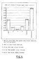
- the optical density (OD) of the black matrix section is preferably maintained to be 3.5 or higher at a practical use level.
- Figure 4 shows the ODs for the red color filter 46R (film thickness: 1.1 ⁇ m), the green color filter 46G (film thickness: 1.1 ⁇ m), the blue color filter 46B (film thickness: 1.1 ⁇ m), and the black matrix 38 (film thickness: 2.0 ⁇ m), alone or placed one upon another.
- the film thickness of the black matrix 38 on the TFT 20 must be 1.0 ⁇ m or larger.
- the film thickness of each layer of the red color filter 46R, the green color filter 46G, and the blue color filter 46B is preferably 1.9 ⁇ m or less, and the film thickness of the black matrix 38 is 1.0 to 2.8 ⁇ m.
- the optical density of the multilayer part on the TFT 20 is 4.44 which is the sum of the ODs of the red color filter 46R, the green color filter 46G, the blue color filter 46B, and the black matrix 38, the blocking of the TFT 20 is ensured.
- the undercoating layer 16 is formed on the glass panel 14. Secondly, the gate electrode 26A and the gate lines 26 are formed on the undercoating layer 16.
- the gate insulation film 28 is formed.
- the semiconductor 24 of the TFT 20 is formed.
- the display electrode 18 is formed.
- the source electrode 32 and the drain electrode 34A of the TFT 20, and the data liens 34 are formed.
- the protective film 36 covering the TFT 20 is formed.
- the black matrix 38 is formed so as to expose the display electrode 18.
- the orientation film 40 is formed, and the rubbing process of the orientation film 40 is performed.
- the red color filter 46R (a section in which there are lines slanted upward to the left) is formed in a position opposed to the black matrix 38 of the array panel 12 and a position opposed to a predetermined pixel region 22 (see Figure 5 (A)).
- the green color filter 46G (a section in which there are lines slanted upward to the right) is formed on the red color filter 46R formed in a position opposed to the black matrix 38 of the array panel 12 and in a position opposed to a predetermined pixel region 22 (see Figure 5 (B)).
- the blue color filter 46B (laterally-striped section) is formed on the green color filter 46G formed in a position opposed to the black matrix 38 of the array panel 12 and in a position opposed to a predetermined pixel region 22 (see Figure 5 (C)).
- the common electrode 52 is formed on the color filter 46.
- the orientation film 54 is formed on the common electrode 52, and the rubbing process of the orientation film 54 is performed.
- the color filter panel 13 and the array panel 12 completed through the above described processes are made to oppose to each other, the peripheries of them are sealed by a resin, a TN liquid crystal 56 is injected into the inside from an injection hole (not shown), the injection hole is sealed, and the deflection plates 17 and 44 are bonded to the glass panels 14 and 42 on both sides, completing the liquid crystal display device 10.
- the height of the spacer corresponds to the cell gap and thus it becomes high (for instance, 5 ⁇ m or higher), which leads to a disadvantage in that the rubbing of the orientation film is not performed around the spacer, whereas in the liquid crystal display device 10 of this embodiment, since projection sections acting as a spacer defining a cell gap are provided on the array panel 12 and the color filter panel 13, respectively, the height of each projecting section can be kept half the height of the conventional spacer or less, and thus the rubbing process of the orientation films 40 and 54 can be reliably performed on the whole surface.
- the second projecting sections 50 are formed by the color filter 46 and the first projecting sections 38A are formed by the black matrix 38, no special process for forming the spacer defining the cell gas is required.
- the black matrix is formed so that the edge of the black matrix is positioned inside of the pixel opening section of the array panel by a predetermined size. If the opening of the black matrix and the pixel opening section of the array panel are of the same size, the electrode of the array panel and the like are exposed if a positional error occurs in the array panel and the color filter panel, considerably degrading the display quality.
- the black matrix is formed in such a way, that the opening area through which light is transmitted will decrease, and hence it is difficult to obtain a light image.
- the black matrix 38 is formed on the array panel 12
- no leakage of light will occur even if a positional error occurs.
- the black matrix 38 can be formed by photolithography, errors in the relative positions between the TFT 20 and other components can be extremely reduced in number, the opening area of the black matrix need not be made small as when the black matrix is formed on the color filter panel. Consequently, the liquid crystal display device 10 of this embodiment can display a light image.
- the second projecting sections 50 are formed by the color filter 46 and the first projecting sections 38A are formed by the black matrix 38, and cell gap Ga can be defined by the second projecting sections 50 and the first projecting sections 38A, an extra process for forming a spacer of resin and the like defining cell gap Ga and the cumbersome process for dispersing transparent spherical spacers can be eliminated, whereby the number of processes can be reduced when compared to the conventional method.
- the second projecting sections 50 are a three-layer structure of red, green, and blue in the above described embodiment, they may be a two-layer structure of any two of red, green, and blue. Further, the order of placing the red, green, and blue colors is not limited to the embodiment, but it may be changed as needed. In addition, the second projecting sections 50 need not be provided so as to correspond to all of the first projecting sections 38A, but they may be thinned out at predetermined intervals.
- the height (the number of steps to be superimposed and the thickness of each layer) of the second projecting sections 50 and the arrangement position of the second projecting sections 50 may be appropriately changed depending on the conditions for the assembly of the array panel 12 and the color filter panel 13 (for instance, the injection condition and the pressurization condition of the TN liquid crystal 56 and the various characteristics of the liquid crystal display device 10 itself).
- the respective thickness of the red color filter 46R, the green color filter 46G, and the blue color filter 46B may all be same or different.
- TFTs are used as the active elements in the above described embodiment, other types of active elements, such as metal-insulator-metal (MIM) switches, varistors, diodes, and the like can, of course, be used.
- MIM metal-insulator-metal
- liquid crystal in the above described embodiment, other types of liquid crystals may, of course, be used.
Landscapes
- Physics & Mathematics (AREA)
- Nonlinear Science (AREA)
- Mathematical Physics (AREA)
- Chemical & Material Sciences (AREA)
- Crystallography & Structural Chemistry (AREA)
- General Physics & Mathematics (AREA)
- Optics & Photonics (AREA)
- Liquid Crystal (AREA)
- Optical Filters (AREA)
Applications Claiming Priority (2)
| Application Number | Priority Date | Filing Date | Title |
|---|---|---|---|
| JP66284/94 | 1994-04-04 | ||
| JP6628494A JP2547523B2 (ja) | 1994-04-04 | 1994-04-04 | 液晶表示装置及びその製造方法 |
Publications (2)
| Publication Number | Publication Date |
|---|---|
| EP0676661A2 true EP0676661A2 (de) | 1995-10-11 |
| EP0676661A3 EP0676661A3 (de) | 1997-03-26 |
Family
ID=13311384
Family Applications (1)
| Application Number | Title | Priority Date | Filing Date |
|---|---|---|---|
| EP95302024A Withdrawn EP0676661A3 (de) | 1994-04-04 | 1995-03-27 | Flüssigkristall-Anzeigevorrichtung und Verfahren zur Herstellung derselben. |
Country Status (6)
| Country | Link |
|---|---|
| US (1) | US5680187A (de) |
| EP (1) | EP0676661A3 (de) |
| JP (1) | JP2547523B2 (de) |
| KR (1) | KR0156655B1 (de) |
| CN (1) | CN1062957C (de) |
| TW (1) | TW279932B (de) |
Cited By (8)
| Publication number | Priority date | Publication date | Assignee | Title |
|---|---|---|---|---|
| EP1018664A4 (de) * | 1997-05-09 | 2003-06-04 | Hitachi Ltd | Flüssigkristallanzeige |
| US6661488B1 (en) | 1997-06-12 | 2003-12-09 | Fujitsu Limited | Vertically-alligned (VA) liquid crystal display device |
| NL1015693C2 (nl) * | 1999-07-14 | 2004-10-05 | Nec Lcd Technologies | Vloeibare-kristallenweergeefeenheid met geleidende afstandsstukken tussen twee substraatstructuren. |
| US7570332B2 (en) | 1998-05-16 | 2009-08-04 | Samsung Electronics Co., Ltd. | Liquid crystal displays having multi-domains and a manufacturing method thereof |
| US7583345B2 (en) | 1999-10-01 | 2009-09-01 | Samsung Electronics Co., Ltd. | Liquid crystal display |
| US7768615B2 (en) | 1997-05-29 | 2010-08-03 | Samsung Electronics Co., Ltd. | Liquid crystal display having wide viewing angle |
| CN102654657A (zh) * | 2011-07-13 | 2012-09-05 | 京东方科技集团股份有限公司 | 降低液晶面板水平黑白线不良发生率的方法 |
| WO2015195222A1 (en) * | 2014-06-18 | 2015-12-23 | Apple Inc. | Display with column spacer structures |
Families Citing this family (81)
| Publication number | Priority date | Publication date | Assignee | Title |
|---|---|---|---|---|
| JP3999824B2 (ja) * | 1995-08-21 | 2007-10-31 | 東芝電子エンジニアリング株式会社 | 液晶表示素子 |
| US6888608B2 (en) * | 1995-09-06 | 2005-05-03 | Kabushiki Kaisha Toshiba | Liquid crystal display device |
| TW373098B (en) * | 1995-09-06 | 1999-11-01 | Toshiba Corp | Liquid crystal exposure component and its fabricating method |
| JPH0980447A (ja) * | 1995-09-08 | 1997-03-28 | Toshiba Electron Eng Corp | 液晶表示素子 |
| JP3556364B2 (ja) * | 1995-12-27 | 2004-08-18 | 富士通ディスプレイテクノロジーズ株式会社 | アクティブマトリクス型液晶表示パネル及び投射型表示装置 |
| US6320639B1 (en) * | 1996-03-11 | 2001-11-20 | Canon Kabushiki Kaisha | Liquid crystal device and process for production thereof |
| JPH1010516A (ja) * | 1996-06-20 | 1998-01-16 | Nec Corp | カラー液晶表示装置 |
| JP2907137B2 (ja) * | 1996-08-05 | 1999-06-21 | 日本電気株式会社 | 液晶表示装置 |
| JPH10104606A (ja) * | 1996-09-27 | 1998-04-24 | Toray Ind Inc | 液晶表示装置 |
| KR19980028453A (ko) * | 1996-10-22 | 1998-07-15 | 김광호 | 평면 구동 방식의 액정 표시 장치 |
| JP3949759B2 (ja) | 1996-10-29 | 2007-07-25 | 東芝電子エンジニアリング株式会社 | カラーフィルタ基板および液晶表示素子 |
| US6940566B1 (en) * | 1996-11-26 | 2005-09-06 | Samsung Electronics Co., Ltd. | Liquid crystal displays including organic passivation layer contacting a portion of the semiconductor layer between source and drain regions |
| KR100447548B1 (ko) * | 1997-04-29 | 2005-01-13 | 삼성전자주식회사 | 액정표시장치 |
| KR19990006215A (ko) * | 1997-06-30 | 1999-01-25 | 김영환 | 액정 표시 소자 및 그 제조방법 |
| KR19990010636A (ko) * | 1997-07-18 | 1999-02-18 | 윤종용 | 액정 표시 장치 및 제조 방법 |
| TW475087B (en) * | 1997-09-12 | 2002-02-01 | Toshiba Corp | Active matrix liquid crystal display device |
| KR100453366B1 (ko) * | 1997-12-19 | 2005-04-06 | 비오이 하이디스 테크놀로지 주식회사 | 액정패널의제조방법 |
| KR100502811B1 (ko) * | 1998-04-10 | 2005-10-14 | 삼성전자주식회사 | 액정표시장치및그제조방법 |
| KR100283511B1 (ko) * | 1998-05-20 | 2001-03-02 | 윤종용 | 광시야각 액정 표시장치 |
| KR20000015175A (ko) * | 1998-08-27 | 2000-03-15 | 김영환 | 액정 표시 장치 |
| KR100601162B1 (ko) * | 1998-08-28 | 2006-10-19 | 삼성전자주식회사 | 액정 표시 장치 |
| JP4094759B2 (ja) * | 1999-02-05 | 2008-06-04 | 株式会社日立製作所 | 液晶表示装置 |
| JP4215905B2 (ja) * | 1999-02-15 | 2009-01-28 | シャープ株式会社 | 液晶表示装置 |
| JP4298131B2 (ja) * | 1999-05-14 | 2009-07-15 | 株式会社半導体エネルギー研究所 | 液晶表示装置の作製方法 |
| US6680487B1 (en) * | 1999-05-14 | 2004-01-20 | Semiconductor Energy Laboratory Co., Ltd. | Semiconductor comprising a TFT provided on a substrate having an insulating surface and method of fabricating the same |
| JP2001117085A (ja) * | 1999-10-15 | 2001-04-27 | Nec Corp | カラー液晶表示パネル及びその製造方法 |
| US6493050B1 (en) * | 1999-10-26 | 2002-12-10 | International Business Machines Corporation | Wide viewing angle liquid crystal with ridge/slit pretilt, post spacer and dam structures and method for fabricating same |
| US6646692B2 (en) * | 2000-01-26 | 2003-11-11 | Semiconductor Energy Laboratory Co., Ltd. | Liquid-crystal display device and method of fabricating the same |
| US6825488B2 (en) * | 2000-01-26 | 2004-11-30 | Semiconductor Energy Laboratory Co., Ltd. | Semiconductor device and manufacturing method thereof |
| US6690437B2 (en) | 2000-04-18 | 2004-02-10 | Semiconductor Energy Laboratory Co., Ltd. | Electro-optical device |
| US6580475B2 (en) * | 2000-04-27 | 2003-06-17 | Semiconductor Energy Laboratory Co., Ltd. | Semiconductor device and method of fabricating the same |
| US7804552B2 (en) * | 2000-05-12 | 2010-09-28 | Semiconductor Energy Laboratory Co., Ltd. | Electro-optical device with light shielding portion comprising laminated colored layers, electrical equipment having the same, portable telephone having the same |
| TW573190B (en) | 2000-08-14 | 2004-01-21 | Samsung Electronics Co Ltd | Liquid crystal display and fabricating method thereof |
| KR100345961B1 (en) * | 2001-01-12 | 2002-08-01 | Samsung Electronics Co Ltd | Liquid crystal display with wide viewing angle |
| US6897918B1 (en) | 2000-09-15 | 2005-05-24 | Toray Industries, Inc. | Color filter with protrusion |
| JP4884586B2 (ja) | 2000-12-18 | 2012-02-29 | 株式会社 日立ディスプレイズ | 液晶表示装置 |
| US6778229B2 (en) * | 2001-10-02 | 2004-08-17 | Fujitsu Display Technologies Corporation | Liquid crystal display device and method of fabricating the same |
| JP4197404B2 (ja) | 2001-10-02 | 2008-12-17 | シャープ株式会社 | 液晶表示装置およびその製造方法 |
| JP2003121850A (ja) * | 2001-10-17 | 2003-04-23 | Hitachi Ltd | 液晶表示装置 |
| US7081704B2 (en) | 2002-08-09 | 2006-07-25 | Semiconductor Energy Laboratory Co., Ltd. | Semiconductor device and manufacturing method thereof |
| KR101012784B1 (ko) * | 2003-06-09 | 2011-02-08 | 삼성전자주식회사 | 표시 장치용 표시판 및 그 표시판을 포함하는 액정 표시장치 |
| KR100989339B1 (ko) * | 2003-06-12 | 2010-10-25 | 삼성전자주식회사 | 액정표시장치 및 이의 제조 방법 |
| JP3888346B2 (ja) * | 2003-10-29 | 2007-02-28 | セイコーエプソン株式会社 | 液晶表示装置及び電子機器 |
| JP4044090B2 (ja) * | 2003-12-26 | 2008-02-06 | シャープ株式会社 | カラーフィルタ基板及びそれを備えた液晶表示装置、並びにカラーフィルタ基板の製造方法 |
| KR101027900B1 (ko) * | 2004-06-04 | 2011-04-08 | 엘지디스플레이 주식회사 | 칼라필터 어레이 기판 및 그 제조방법 |
| TWI264603B (en) * | 2004-07-19 | 2006-10-21 | Chunghwa Picture Tubes Ltd | Substrate structure for forming alignment film thereon by ink-jet printing and liquid crystal panel formed by using the same |
| KR101064189B1 (ko) * | 2004-08-03 | 2011-09-14 | 삼성전자주식회사 | 컬러필터 기판, 표시패널 및 이의 제조방법 |
| CN100371796C (zh) * | 2005-03-15 | 2008-02-27 | 友达光电股份有限公司 | 液晶显示装置 |
| KR101114233B1 (ko) * | 2005-04-29 | 2012-03-06 | 엘지디스플레이 주식회사 | 액정표시패널 및 그 제조방법 |
| KR20070012084A (ko) * | 2005-07-22 | 2007-01-25 | 삼성전자주식회사 | 컬러필터 기판과 이를 포함하는 액정표시패널 그리고이들의 제조방법 |
| KR20070014584A (ko) * | 2005-07-29 | 2007-02-01 | 삼성전자주식회사 | 표시 패널 |
| JP4455449B2 (ja) * | 2005-08-05 | 2010-04-21 | 東芝モバイルディスプレイ株式会社 | 液晶表示素子の製造方法 |
| JP5079995B2 (ja) | 2005-08-26 | 2012-11-21 | 株式会社ジャパンディスプレイイースト | 透過型液晶表示装置およびその製造方法 |
| KR101183386B1 (ko) * | 2005-09-28 | 2012-09-14 | 엘지디스플레이 주식회사 | 액정 표시 장치 및 이의 제조 방법 |
| JP5174450B2 (ja) * | 2007-12-18 | 2013-04-03 | パナソニック液晶ディスプレイ株式会社 | 液晶表示装置 |
| US8749496B2 (en) | 2008-12-05 | 2014-06-10 | Apple Inc. | Integrated touch panel for a TFT display |
| CN101825802B (zh) * | 2009-03-06 | 2011-12-28 | 北京京东方光电科技有限公司 | 彩膜基板及其制造方法 |
| JP5561576B2 (ja) * | 2009-06-11 | 2014-07-30 | 大日本印刷株式会社 | 液晶表示装置用カラーフィルタおよび液晶表示装置 |
| KR101307555B1 (ko) | 2009-12-28 | 2013-09-12 | 엘지디스플레이 주식회사 | 평판 표시장치 제조 방법 |
| US9142533B2 (en) * | 2010-05-20 | 2015-09-22 | Taiwan Semiconductor Manufacturing Company, Ltd. | Substrate interconnections having different sizes |
| CN102109628A (zh) * | 2011-01-28 | 2011-06-29 | 深圳市华星光电技术有限公司 | 彩色滤光片构造及其制造方法 |
| US9646923B2 (en) | 2012-04-17 | 2017-05-09 | Taiwan Semiconductor Manufacturing Company, Ltd. | Semiconductor devices, methods of manufacture thereof, and packaged semiconductor devices |
| US9425136B2 (en) | 2012-04-17 | 2016-08-23 | Taiwan Semiconductor Manufacturing Company, Ltd. | Conical-shaped or tier-shaped pillar connections |
| US9299674B2 (en) | 2012-04-18 | 2016-03-29 | Taiwan Semiconductor Manufacturing Company, Ltd. | Bump-on-trace interconnect |
| US9395583B2 (en) * | 2012-06-06 | 2016-07-19 | Apple Inc. | Column spacer design for a display incorporating a third metal layer |
| US9111817B2 (en) | 2012-09-18 | 2015-08-18 | Taiwan Semiconductor Manufacturing Company, Ltd. | Bump structure and method of forming same |
| CN103913892B (zh) * | 2012-12-31 | 2017-05-03 | 厦门天马微电子有限公司 | 一种液晶显示面板 |
| CN103901663A (zh) * | 2014-03-28 | 2014-07-02 | 南京中电熊猫液晶显示科技有限公司 | 一种液晶显示器的彩膜基板 |
| WO2015160377A1 (en) | 2014-04-16 | 2015-10-22 | Wrostix Technologies Llc | Structure for pixelated self-capacitance |
| US9367188B2 (en) | 2014-05-23 | 2016-06-14 | Apple Inc. | RC matching in a touch screen |
| WO2015183334A1 (en) | 2014-05-28 | 2015-12-03 | Pylemta Management Llc | Narrow border touch screen |
| KR102189578B1 (ko) * | 2014-07-30 | 2020-12-14 | 삼성디스플레이 주식회사 | 액정 표시 패널 및 그 제조 방법 |
| KR102334808B1 (ko) | 2015-04-30 | 2021-12-03 | 삼성디스플레이 주식회사 | 표시 패널 |
| CN104932153A (zh) * | 2015-06-29 | 2015-09-23 | 京东方科技集团股份有限公司 | 曲面显示基板和曲面显示装置 |
| CN105204219B (zh) * | 2015-10-27 | 2019-05-17 | 南京中电熊猫液晶显示科技有限公司 | 一种液晶显示基板的彩膜基板 |
| CN105223727B (zh) * | 2015-10-27 | 2019-02-01 | 南京中电熊猫液晶显示科技有限公司 | 一种液晶显示器的彩膜基板 |
| US10394014B2 (en) | 2016-03-22 | 2019-08-27 | Amazon Technologies, Inc. | Integrated black matrix including color filter materials |
| US20180053791A1 (en) * | 2016-08-19 | 2018-02-22 | Innolux Corporation | Array substrate and display device with the array substrate |
| CN107768383B (zh) * | 2016-08-19 | 2021-06-04 | 群创光电股份有限公司 | 阵列基板及包括此阵列基板的显示装置 |
| CN107045222A (zh) * | 2016-12-29 | 2017-08-15 | 惠科股份有限公司 | 液晶面板及其制造方法 |
| WO2023039823A1 (zh) * | 2021-09-17 | 2023-03-23 | 京东方科技集团股份有限公司 | 一种显示面板及其制备方法、显示装置 |
Family Cites Families (12)
| Publication number | Priority date | Publication date | Assignee | Title |
|---|---|---|---|---|
| JPS60159823A (ja) * | 1984-01-31 | 1985-08-21 | Matsushita Electric Ind Co Ltd | カラ−液晶表示装置 |
| JPS60164723A (ja) * | 1984-02-07 | 1985-08-27 | Seiko Instr & Electronics Ltd | 液晶表示装置 |
| JPS617823A (ja) * | 1984-06-22 | 1986-01-14 | Canon Inc | 液晶パネル |
| JPS63101823A (ja) * | 1986-10-17 | 1988-05-06 | Alps Electric Co Ltd | 液晶表示素子 |
| US5150232A (en) * | 1988-10-04 | 1992-09-22 | Asahi Glass Company Ltd. | Active matrix liquid crystal display element and projection type active matrix liquid crystal display device |
| JPH0359522A (ja) * | 1989-07-28 | 1991-03-14 | Hitachi Ltd | 液晶表示装置 |
| JPH03287234A (ja) * | 1990-04-04 | 1991-12-17 | Hitachi Ltd | カラー液晶素子 |
| JP3011993B2 (ja) * | 1990-10-26 | 2000-02-21 | 株式会社リコー | カラー液晶素子 |
| JPH05158067A (ja) * | 1991-12-03 | 1993-06-25 | Stanley Electric Co Ltd | 液晶表示装置とその製造方法 |
| JPH05249478A (ja) * | 1991-12-25 | 1993-09-28 | Toshiba Corp | 液晶表示装置 |
| JPH05196946A (ja) * | 1992-01-20 | 1993-08-06 | Sharp Corp | 液晶表示装置 |
| JP2812851B2 (ja) * | 1993-03-24 | 1998-10-22 | シャープ株式会社 | 反射型液晶表示装置 |
-
1994
- 1994-04-04 JP JP6628494A patent/JP2547523B2/ja not_active Expired - Lifetime
- 1994-12-22 TW TW083112054A patent/TW279932B/zh not_active IP Right Cessation
-
1995
- 1995-03-16 CN CN95102492A patent/CN1062957C/zh not_active Expired - Lifetime
- 1995-03-21 KR KR1019950005894A patent/KR0156655B1/ko not_active Expired - Lifetime
- 1995-03-27 EP EP95302024A patent/EP0676661A3/de not_active Withdrawn
- 1995-04-04 US US08/416,280 patent/US5680187A/en not_active Expired - Lifetime
Cited By (28)
| Publication number | Priority date | Publication date | Assignee | Title |
|---|---|---|---|---|
| EP1018664A4 (de) * | 1997-05-09 | 2003-06-04 | Hitachi Ltd | Flüssigkristallanzeige |
| US7349049B2 (en) | 1997-05-09 | 2008-03-25 | Hitachi, Ltd | Liquid crystal display apparatus |
| US7088412B2 (en) | 1997-05-09 | 2006-08-08 | Hitachi, Ltd. | Liquid crystal display apparatus |
| US9041891B2 (en) | 1997-05-29 | 2015-05-26 | Samsung Display Co., Ltd. | Liquid crystal display having wide viewing angle |
| US7768615B2 (en) | 1997-05-29 | 2010-08-03 | Samsung Electronics Co., Ltd. | Liquid crystal display having wide viewing angle |
| US7227606B2 (en) | 1997-06-12 | 2007-06-05 | Sharp Kabushiki Kaisha | Vertically-alligned (VA) liquid crystal display device |
| USRE43123E1 (en) | 1997-06-12 | 2012-01-24 | Sharp Kabushiki Kaisha | Vertically-aligned (VA) liquid crystal display device |
| US7167224B1 (en) | 1997-06-12 | 2007-01-23 | Sharp Kabushiki Kaisha | Vertically-aligned (VA) liquid crystal display device |
| US7304703B1 (en) | 1997-06-12 | 2007-12-04 | Sharp Kabushiki Kaisha | Vertically-aligned (VA) liquid crystal display device |
| US6661488B1 (en) | 1997-06-12 | 2003-12-09 | Fujitsu Limited | Vertically-alligned (VA) liquid crystal display device |
| US8553188B2 (en) | 1997-06-12 | 2013-10-08 | Sharp Kabushiki Kaisha | Liquid crystal display device |
| US7224421B1 (en) | 1997-06-12 | 2007-05-29 | Sharp Kabushiki Kaisha | Vertically-aligned (VA) liquid crystal display device |
| US8134671B2 (en) | 1997-06-12 | 2012-03-13 | Sharp Kabushiki Kaisha | Liquid crystal display device |
| US7760305B2 (en) | 1997-06-12 | 2010-07-20 | Sharp Kabushiki Kaisha | Liquid crystal display device with multiple alignment structures |
| US6724452B1 (en) | 1997-06-12 | 2004-04-20 | Fujitsu Display Technologies Corporation | Vertically aligned (VA) liquid crystal display device |
| US7821603B2 (en) | 1997-06-12 | 2010-10-26 | Sharp Kabushiki Kaisha | Vertically-alligned (VA) liquid crystal display device |
| US7965363B2 (en) | 1997-06-12 | 2011-06-21 | Sharp Kabushiki Kaisha | Vertically-aligned (VA) liquid crystal display device |
| US7573554B2 (en) | 1998-05-16 | 2009-08-11 | Samsung Electronics Co., Ltd. | Liquid crystal displays having multi-domains and a manufacturing method thereof |
| US7570332B2 (en) | 1998-05-16 | 2009-08-04 | Samsung Electronics Co., Ltd. | Liquid crystal displays having multi-domains and a manufacturing method thereof |
| NL1015693C2 (nl) * | 1999-07-14 | 2004-10-05 | Nec Lcd Technologies | Vloeibare-kristallenweergeefeenheid met geleidende afstandsstukken tussen twee substraatstructuren. |
| US7583345B2 (en) | 1999-10-01 | 2009-09-01 | Samsung Electronics Co., Ltd. | Liquid crystal display |
| US8174651B2 (en) | 1999-10-01 | 2012-05-08 | Samsung Electronics Co., Ltd. | Liquid crystal display |
| US8456597B2 (en) | 1999-10-01 | 2013-06-04 | Samsung Display Co., Ltd. | Liquid crystal display |
| US8817213B2 (en) | 1999-10-01 | 2014-08-26 | Samsung Display Co., Ltd. | Liquid crystal display |
| US9557612B2 (en) | 1999-10-01 | 2017-01-31 | Samsung Display Co., Ltd. | Liquid crystal display |
| CN102654657A (zh) * | 2011-07-13 | 2012-09-05 | 京东方科技集团股份有限公司 | 降低液晶面板水平黑白线不良发生率的方法 |
| WO2015195222A1 (en) * | 2014-06-18 | 2015-12-23 | Apple Inc. | Display with column spacer structures |
| US9482905B2 (en) | 2014-06-18 | 2016-11-01 | Apple Inc. | Display with column spacer structures |
Also Published As
| Publication number | Publication date |
|---|---|
| KR0156655B1 (ko) | 1998-11-16 |
| TW279932B (de) | 1996-07-01 |
| CN1062957C (zh) | 2001-03-07 |
| JPH07281195A (ja) | 1995-10-27 |
| JP2547523B2 (ja) | 1996-10-23 |
| US5680187A (en) | 1997-10-21 |
| CN1119743A (zh) | 1996-04-03 |
| KR950029813A (ko) | 1995-11-24 |
| EP0676661A3 (de) | 1997-03-26 |
Similar Documents
| Publication | Publication Date | Title |
|---|---|---|
| US5680187A (en) | Liquid crystal display device and method for manufacturing the same | |
| US10690971B2 (en) | Liquid crystal display device | |
| US7697106B2 (en) | Liquid crystal display device and method of manufacturing the same | |
| KR100269196B1 (ko) | 액정표시장치 | |
| KR100848078B1 (ko) | 액정표시장치용 기판, 액정표시장치 및 액정표시장치용기판의 제조 방법 | |
| US6667790B2 (en) | Liquid crystal display having particular spacer | |
| KR100362016B1 (ko) | 액정표시장치 | |
| KR100403645B1 (ko) | 액정표시패널 및 그 제조방법 | |
| US10031372B2 (en) | Liquid crystal display device | |
| US6768531B2 (en) | Liquid crystal display device | |
| US20050190335A1 (en) | Liquid crystal display device having an injection hole for liquid crystal | |
| US20020005929A1 (en) | Liquid crystal display device | |
| US20090103021A1 (en) | Liquid crystal display panel | |
| US6954250B2 (en) | Liquid crystal display and manufacturing method thereof | |
| US20070188690A1 (en) | Liquid crystal display device | |
| KR20030082141A (ko) | 패턴드 스페이서를 가지는 액정표시장치 | |
| KR100832202B1 (ko) | 액정 표시 장치용 기판 및 그것을 구비한 액정 표시 장치 | |
| JP2006039137A (ja) | カラーフィルタ基板、および表示装置 | |
| US20060044502A1 (en) | Liquid crystal display | |
| JP3129294B2 (ja) | アクティブマトリクス液晶表示装置 | |
| JPH1184386A (ja) | アクティブマトリクス型液晶表示装置 | |
| JP2000298280A (ja) | 液晶表示素子 | |
| US6762814B2 (en) | In-plane switching mode liquid crystal display device and method of fabricating the same | |
| KR100510188B1 (ko) | 액정표시패널 및 그 제조방법 | |
| JP2004219827A (ja) | 液晶表示装置 |
Legal Events
| Date | Code | Title | Description |
|---|---|---|---|
| PUAI | Public reference made under article 153(3) epc to a published international application that has entered the european phase |
Free format text: ORIGINAL CODE: 0009012 |
|
| AK | Designated contracting states |
Kind code of ref document: A2 Designated state(s): DE FR GB |
|
| 17P | Request for examination filed |
Effective date: 19960213 |
|
| PUAL | Search report despatched |
Free format text: ORIGINAL CODE: 0009013 |
|
| RHK1 | Main classification (correction) |
Ipc: G02F 1/1339 |
|
| AK | Designated contracting states |
Kind code of ref document: A3 Designated state(s): DE FR GB |
|
| 17Q | First examination report despatched |
Effective date: 20030326 |
|
| STAA | Information on the status of an ep patent application or granted ep patent |
Free format text: STATUS: THE APPLICATION IS DEEMED TO BE WITHDRAWN |
|
| 18D | Application deemed to be withdrawn |
Effective date: 20030806 |