EP0678910A2 - Système d'inspection de plaquettes semi-conductrices - Google Patents
Système d'inspection de plaquettes semi-conductrices Download PDFInfo
- Publication number
- EP0678910A2 EP0678910A2 EP95105931A EP95105931A EP0678910A2 EP 0678910 A2 EP0678910 A2 EP 0678910A2 EP 95105931 A EP95105931 A EP 95105931A EP 95105931 A EP95105931 A EP 95105931A EP 0678910 A2 EP0678910 A2 EP 0678910A2
- Authority
- EP
- European Patent Office
- Prior art keywords
- semiconductor wafer
- camera
- checked
- hemispherical
- lighting
- Prior art date
- Legal status (The legal status is an assumption and is not a legal conclusion. Google has not performed a legal analysis and makes no representation as to the accuracy of the status listed.)
- Granted
Links
Images

Classifications
-
- H—ELECTRICITY
- H10—SEMICONDUCTOR DEVICES; ELECTRIC SOLID-STATE DEVICES NOT OTHERWISE PROVIDED FOR
- H10P—GENERIC PROCESSES OR APPARATUS FOR THE MANUFACTURE OR TREATMENT OF DEVICES COVERED BY CLASS H10
- H10P74/00—Testing or measuring during manufacture or treatment of wafers, substrates or devices
- H10P74/27—Structural arrangements therefor
-
- G—PHYSICS
- G01—MEASURING; TESTING
- G01R—MEASURING ELECTRIC VARIABLES; MEASURING MAGNETIC VARIABLES
- G01R31/00—Arrangements for testing electric properties; Arrangements for locating electric faults; Arrangements for electrical testing characterised by what is being tested not provided for elsewhere
- G01R31/28—Testing of electronic circuits, e.g. by signal tracer
- G01R31/302—Contactless testing
- G01R31/308—Contactless testing using non-ionising electromagnetic radiation, e.g. optical radiation
- G01R31/311—Contactless testing using non-ionising electromagnetic radiation, e.g. optical radiation of integrated circuits
-
- G—PHYSICS
- G01—MEASURING; TESTING
- G01N—INVESTIGATING OR ANALYSING MATERIALS BY DETERMINING THEIR CHEMICAL OR PHYSICAL PROPERTIES
- G01N21/00—Investigating or analysing materials by the use of optical means, i.e. using sub-millimetre waves, infrared, visible or ultraviolet light
- G01N21/84—Systems specially adapted for particular applications
- G01N21/88—Investigating the presence of flaws or contamination
- G01N21/8806—Specially adapted optical and illumination features
-
- G—PHYSICS
- G01—MEASURING; TESTING
- G01N—INVESTIGATING OR ANALYSING MATERIALS BY DETERMINING THEIR CHEMICAL OR PHYSICAL PROPERTIES
- G01N21/00—Investigating or analysing materials by the use of optical means, i.e. using sub-millimetre waves, infrared, visible or ultraviolet light
- G01N21/84—Systems specially adapted for particular applications
- G01N21/88—Investigating the presence of flaws or contamination
- G01N21/95—Investigating the presence of flaws or contamination characterised by the material or shape of the object to be examined
- G01N21/9501—Semiconductor wafers
-
- G—PHYSICS
- G01—MEASURING; TESTING
- G01R—MEASURING ELECTRIC VARIABLES; MEASURING MAGNETIC VARIABLES
- G01R31/00—Arrangements for testing electric properties; Arrangements for locating electric faults; Arrangements for electrical testing characterised by what is being tested not provided for elsewhere
- G01R31/26—Testing of individual semiconductor devices
- G01R31/265—Contactless testing
- G01R31/2656—Contactless testing using non-ionising electromagnetic radiation, e.g. optical radiation
-
- H—ELECTRICITY
- H10—SEMICONDUCTOR DEVICES; ELECTRIC SOLID-STATE DEVICES NOT OTHERWISE PROVIDED FOR
- H10P—GENERIC PROCESSES OR APPARATUS FOR THE MANUFACTURE OR TREATMENT OF DEVICES COVERED BY CLASS H10
- H10P74/00—Testing or measuring during manufacture or treatment of wafers, substrates or devices
- H10P74/20—Testing or measuring during manufacture or treatment of wafers, substrates or devices characterised by the properties tested or measured, e.g. structural or electrical properties
- H10P74/203—Structural properties, e.g. testing or measuring thicknesses, line widths, warpage, bond strengths or physical defects
Definitions
- the invention relates to a device for checking semiconductor wafers.
- the semiconductor wafers When manufacturing integrated semiconductor circuits, the semiconductor wafers must always be checked for perfect condition. Defective semiconductor wafers are to be recognized so that they can either be completely excluded from the further production process or that they can be reworked accordingly before the further production process and then, provided that there are no errors, can be reintroduced into the normal production process.
- Such checks of semiconductor wafers for perfect condition e.g. check for particle freedom, i.e. free of dirt and deposits, check of applied lacquer layers, etc.
- check for particle freedom i.e. free of dirt and deposits, check of applied lacquer layers, etc.
- the object of the present invention is therefore to create a device with the aid of which the checking process can be automated.
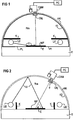
- FIG. 1 shows a first embodiment of the device, which can be arranged, for example, on a table T (also applies to the other two embodiments according to FIGS. 2 and 3) or another suitable base with a fixed stand.
- the device has a device E for receiving the semiconductor wafer WF to be checked and a base plate P1, which, however, is not absolutely necessary.
- the device E can be part of the base plate P1.
- it can also be arranged on the base plate P1 or embedded therein.
- the device also has a hemispherical covering device HK with an interior Rm which is largely closed off by means of the base plate P1.
- annular illumination device Lt1 is arranged within this closed space Rm, which is used for direct illumination of the semiconductor wafer WF to be checked.
- the ring shape enables uniform illumination of the semiconductor wafer WF.
- the hemispherical covering device HK has a surface K1 within the closed space Rm which absorbs incident light Lt.
- a further covering device K is arranged above the lighting device Lt1, which absorbs incident light Lt. It is designed in such a way that the semiconductor wafer WF can be directly illuminated by means of the lighting device Lt1, while the hemispherical cover HK is largely covered with respect to the direct light of the lighting device Lt1. As a result of these requirements, it is expedient, particularly in the case of a ring-shaped design of the lighting device Lt1, to also design the further cover device K as a ring.
- a camera CAM is arranged on the hemispherical cover device HK vertically above the center of the device E for receiving the pane WF to be checked so that its objective Obj looks into the closed space Rm, in particular at the point at which the device to be checked is in operation Semiconductor wafer WF is located.
- the camera CAM can be arranged in such a way that its objective Obj protrudes into the closed space Rm, as shown in FIG. 1, or in such a way that the edge of its objective Obj is approximately flush with the hemispherical cover HK.
- the camera CAM is connected to an evaluation device PC, which is used to control the camera and to receive, store, process and output data transmitted by the camera CAM.
- This data can be transmitted analog (in the form of "pictures") or digitally, provided the camera CAM is already equipped for digital transmission (e.g. if it has an A / D converter).
- the evaluation device PC is typically a computer device such as personnel Computer or data processing equipment. However, it is also conceivable that it is formed exclusively from hardware that executes a corresponding method.
- the surface K1 of the hemispherical cover HK which absorbs the light Lt is black.
- the light Lt emitted by the lighting device Lt1 is white.
- the further covering device K has a black surface.
- the surface of the base plate P1 is black on its side facing the hemispherical covering device HK.
- the checking process can be automated, for example with the aid of the method described below.
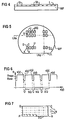
- semiconductor wafers WF often have a so-called flat Ft (see FIG. 5) (ie a region of the round semiconductor wafer WF is flattened), the following method assumes that the semiconductor wafers to be checked have such a flat Ft. Furthermore, it is based on the fact that the semiconductor chips to be formed on the semiconductor wafers WF in the manufacturing process are rectangular, possibly square, and that they are aligned parallel to the flat Ft.
- the semiconductor chips to be manufactured by means of the semiconductor wafer WF to be controlled are integrated semiconductor memories which are known to be independent of their type of memory ⁇ e.g. B. volatile memories such as DRAM's, SRAM's, non-volatile memories (NV memories) such as ROM's, PROM's, EEPROM's ⁇ , large areas SQ (see FIG. 5) of regular structures (the so-called memory cell blocks or memory cell arrays) and areas of irregular structures which e.g. B. the so-called peripheral circuits, such as. B. Decoder and amplifier and the pads (pads) included.
- the areas of regular structures SQ generally comprise approximately 80 to 95% of the total memory chip.
- areas of the semiconductor chips WF are arranged between the individual chips, which serve to divide the (finished) semiconductor wafer WF for mounting the individual chips in a housing, in a chip card or the like (generally designated by a scoring frame).
- a scoring frame a chip card or the like
- the semiconductor wafer WF (shown in FIG. 4) has at least one layer which already contains structures St of the semiconductor chips to be produced, and, as the uppermost layer, a lacquer layer L (for further structuring steps) to be checked are (shown in Fig. 4).
- the procedure is as follows: The semiconductor wafer WF is illuminated directly by the lighting device Lt1, for. B. with white light.
- the lacquer layer L applied to the semiconductor wafer WF reflects the light Lt.
- the reflectance R of the reflected light Lt is now determined according to the following procedure (here, the degree of brightness R is understood as the measure of the brightness, that of Semiconductor wafer WF hits or works on the lens of the CAM camera): First of all, a first line LNx, which serves as a measuring line and runs parallel to the flat Ft at a given distance, is simulated on the surface of the lacquer L of the semiconductor wafer WF by means of the evaluation device PC, ie "thought".
- the brightness of the semiconductor wafer WF ie the value of the reflectance R, is not shown along this imaginary line LNx at selected points Px (“pixels”) For reasons of clarity) determined by the camera CAM and evaluation device PC and, together with the position value x of these points Px, temporarily stored in the evaluation device PC.
- this imaginary line LNx there are mostly values of the determined and measured reflectance R, which are below a predetermined minimum value Rmin, the determined and temporarily stored data regarding this line LNx are rejected as unusable. It is assumed that the line LNx does not run predominantly through the large areas SQ of the regular structures, but through the areas of irregular structures or through a Ritz frame. By convention, these areas and the Ritz frame (called "U”; see FIG. 5) should not be checked. Instead of the imaginary line LNx measured so far, another "imaginary" line LNx1 is now selected and used at a given distance from this imaginary line LNx (not shown in FIG. 5 for reasons of clarity), with respect to which the reflectance R is likewise determined and buffered together with the associated position values x as with the originally used imaginary line LNx.
- the position values x (for the imaginary line LNx) and y (for the imaginary line LNy) of the respective measuring points of these lines LNx and LNy are already temporarily stored.
- the position values are based on the position of the flat Ft. If possible, the measuring points Px and Py should have been placed so close to each other that the boundaries between the respective areas SQ of regular structures to the areas U (irregular structures and scratches) are as precise as possible (ie, via their associated values of the reflectance R) Frame) are recorded.
- FIG. 6 shows an example of the course of the measured values of the reflectance R along the imaginary line LNx.
- SQ stands for the (presumably rectangular) large areas SQ of regular structures while “U” stands for the (smaller) areas of irregular structures and the respective Ritz frames.
- X and "Y” used (in brackets) are explained below.
- the picture is based on the fact that the large areas SQ of regular structures normally have high values of the reflectance R, while the areas U usually have a significantly lower value of the reflectance R.
- the determination is carried out in a mathematically easy manner from the information that the large areas SQ form rectangles which are in the x and y directions (ie parallel and perpendicular to the flat Ft and thus parallel or perpendicular to the imaginary lines LNx, LNy ) Repeat regularly and from the assessment criterion that only those position points x or y of the two imaginary lines LNx, LNy are taken into account whose associated value of the reflectance R does exceed a predetermined maximum value Rmax, but which at the same time is adjacent points of such position values x and y are below this maximum value Rmax. All position points x and y, whose associated value of the degree of reflection R lies below this maximum value Rmax, are masked out by the further method as areas U which cannot be checked.
- At least one measuring line LN is "placed" parallel to an edge (shown in FIG. 7 by way of example using four measuring lines LN: parallel to the edge AB or CD), eg . B. parallel to the longer edge.
- the respective value of the reflectance R is determined and temporarily stored by means of the camera CAM and the evaluation device PC at predetermined measuring points 1, 2, 3,.
- the two curves shown in FIG. 8 result, for example.
- the measurement points 1 to 23 are plotted on the abscissa.
- the respective value of the reflectance R can be read off the ordinate.
- the values of the reflectance R entered with "x" are values along a first measuring line LN. As the possible criteria for recognizing whether an error is present or not, shown below, no error can be identified along this measurement line. There are different values of the reflectance R (caused by the different structures within the area SQ, below the lacquer layer L). However, as can be seen from the assessment criteria mentioned below, these are in the range of the usual values to be expected, so that the controlled area SQ can be rated as "good” with respect to this measurement line LN. The values of the reflectance R have a periodic course.
- the values of the reflectance R entered in FIG. 8 with "o" are measured values along a second measuring line LN, for example of the same area SQ.
- the measuring points 4 and 11 are striking.
- the value of the reflectance R at the measuring point 4 (ie within the first period) is clearly above the other measuring points, in particular also with regard to their local maximum values within each of the further periods 2... There is an error here that is caused by a white particle is caused. Because a white particle emits the light Lt better than the other parts of the lacquer layer L, this value is particularly high.
- the value of the reflectance R at measuring point 11, which (coincidentally) is located at the transition from the second to the third period, is particularly low compared to the remaining measuring points, in particular with the minimum values in the individual periods.
- the lacquer layer L closes at this point is thin or even has a hole. This could result in structuring errors such as under-etching etc. during the further production of the memory chip.
- the measured values along the second measuring line LN show two errors, each of which leads to a corresponding sorting out of the semiconductor wafer WF upon detection and possibly to reworking.
- the evaluation device PC uses evaluation criteria to determine whether the rectangular area SQ under investigation, and thus the entire semiconductor wafer WF, is in order or defective.
- the results can then be output by means of the evaluation device PC.
- the following assessment criteria in particular can be used when assessing whether the controlled semiconductor wafer WF or its rectangular areas SQ are in order or not: It can be determined, either separately for each measuring line LN of a surface SQ, or for all measuring lines LN of the surface SQ in question, the maximum values of the reflectance R of the individual periods occurring and then checked whether they are more than a predetermined, permissible Distinguish difference value from each other. If this is the case, an error is assumed; the relevant value and the associated coordinates are temporarily stored and, if necessary, output or further processed.
- Figure 2 shows a second embodiment of the device according to the invention. It is constructed similarly to the first embodiment, but differs significantly from this in some respects.
- the second embodiment also has a device E for receiving the semiconductor wafer WF to be checked and an illumination device Lt2. However, this serves to indirectly illuminate the semiconductor wafer WF.
- the hemispherical covering device HK already presented is also present, but with a surface K2 in its interior which reflects incident light Lt to a high degree. It is therefore preferably white.
- a further incident light Lt absorbing cover device K is arranged, which is designed such that it prevents direct light incidence on the device E together with the semiconductor wafer WF, that is, the Semiconductor wafer WF can only be illuminated indirectly with the lighting device Lt2 by reflection of the light Lt at the hemispherical covering device HK.
- a camera CAM is also arranged on the hemispherical cover HK so that its objective Obj looks into the space Rm within the hemispherical cover device HK. With regard to the center of the device E for receiving the semiconductor wafer WF, the camera CAM is however not arranged vertically as in the first embodiment according to FIG.
- the camera cannot reflect directly or indirectly on the semiconductor wafer WF, which would interfere with the detection of the values of the reflectance R. It is also advantageous if the lens Obj of the camera CAM is equipped with a red filter F, which increases the contrast of the received image.
- the camera CAM is connected to an evaluation device PC, which is used to control the camera CAM and to receive, process, temporarily store and output the data or images transmitted by the camera CAM.
- the light from the lighting devices Lt1 and Lt2 is white.
- the further covering devices K have a black surface.
- Further parts of the camera CAM located within the hemispherical covering device HK are arranged, if they exist at all, in such a way that, viewed from the semiconductor wafer WF or the device E, they are covered by the objective Obj.
- it is advantageous in terms of uniform illumination if the lighting devices Lt1 or Lt2 and / or the further covers K are ring-shaped.
- a base plate P1 is not absolutely necessary (outside, perhaps for mechanical reasons, for reasons of stability or for reasons of easier processing of recorded images). However, if it is available, it should be light-absorbing, preferably black.
- the second embodiment has the following advantage over the first embodiment: it results in defects in Semiconductor wafers that cannot be made visible when the camera CAM is standing upright and / or when the semiconductor wafer WF is directly irradiated and are therefore not recognizable.
- this second embodiment ie by means of indirect lighting and by means of an inclined camera CAM, these defects can also be recognized in most cases, so that timely reworking of the semiconductor wafers in question is possible, which in turn increases the yield of the semiconductor memories to be produced and thus lowers overall production costs.
- a third embodiment of the device shown in FIG. 3, combines the advantages of the first two embodiments, namely detection of defects both with camera CAM1 standing upright and direct illumination and with camera CAM2 inclined and indirect lighting. The embodiment is described below with reference to FIG. 3.
- the second color Rt is preferably red.
- a hemispherical covering device HK which is also part of this third device, has in its interior Rm a surface K3, which is also of the second color Rt, that is to say preferably red.
- the hemispherical cover HK forms a largely closed interior space Rm by means of a base plate Pl, which is not absolutely necessary.
- This base plate Pl can have the second color Rt on its surface facing the space Rm, ie preferably red.
- the surface could have a different design but also be black.
- a further covering device K which is opaque, is arranged above the first lighting device Lt1. It is designed such that on the one hand the semiconductor wafer WF can be directly illuminated by means of the first lighting device Lt1 and that on the other hand this semiconductor wafer WF can only be illuminated indirectly by the second lighting device Lt2.
- a first camera CAM1 is arranged on the hemispherical covering device HK so that its objective Obj looks into the space Rm within the hemispherical covering device HK and there onto the device E.
- a camera CAM2 is arranged on the hemispherical covering device HK so that its objective Obj looks into the space Rm within the hemispherical covering device HK and there onto the device E.
- the second camera CAM2 is arranged at an angle ⁇ with respect to the center point of the device E, which angle is greater than 0 ° and maximally so large that the second camera CAM2 does not come into contact with the first camera CAM1.
- Both cameras CAM1, CAM2 are connected to an evaluation device PC, which is used to control the cameras CAM1, CAM2, as well as for recording, for intermediate storage, for further processing and for outputting data or images obtained from the cameras CAM1, CAM2.
- the system with the complementary colors Gn, Rt of the lighting devices Lt1 , Lt2 and the correspondingly designed surfaces of the covering device HK and the base plate P1.
- At least one of the two lighting devices Lt1, Lt2 and / or the further covering device K is ring-shaped or is arranged.
- the device E for receiving the semiconductor wafers WF can also be advantageously designed in various ways: as a component of the base plate P1, arranged on the base plate P1 or embedded therein (P1).
- the angle ⁇ at which the second camera CAM2 is arranged with respect to the center of the device E is 40 ° to 70 °.
- An arrangement of 60 ° is optimal.
Landscapes
- Physics & Mathematics (AREA)
- General Physics & Mathematics (AREA)
- Health & Medical Sciences (AREA)
- Immunology (AREA)
- Engineering & Computer Science (AREA)
- Life Sciences & Earth Sciences (AREA)
- Chemical & Material Sciences (AREA)
- Analytical Chemistry (AREA)
- Biochemistry (AREA)
- General Health & Medical Sciences (AREA)
- Pathology (AREA)
- Electromagnetism (AREA)
- Toxicology (AREA)
- Computer Hardware Design (AREA)
- Microelectronics & Electronic Packaging (AREA)
- Computer Vision & Pattern Recognition (AREA)
- General Engineering & Computer Science (AREA)
- Testing Or Measuring Of Semiconductors Or The Like (AREA)
- Investigating Materials By The Use Of Optical Means Adapted For Particular Applications (AREA)
- Crystals, And After-Treatments Of Crystals (AREA)
- Investigating Or Analysing Materials By Optical Means (AREA)
- Packaging Frangible Articles (AREA)
Applications Claiming Priority (2)
| Application Number | Priority Date | Filing Date | Title |
|---|---|---|---|
| DE4413832A DE4413832C2 (de) | 1994-04-20 | 1994-04-20 | Vorrichtungen zur Kontrolle von Halbleiterscheiben |
| DE4413832 | 1994-04-20 |
Publications (3)
| Publication Number | Publication Date |
|---|---|
| EP0678910A2 true EP0678910A2 (fr) | 1995-10-25 |
| EP0678910A3 EP0678910A3 (fr) | 1996-04-17 |
| EP0678910B1 EP0678910B1 (fr) | 2001-06-27 |
Family
ID=6516017
Family Applications (1)
| Application Number | Title | Priority Date | Filing Date |
|---|---|---|---|
| EP95105931A Expired - Lifetime EP0678910B1 (fr) | 1994-04-20 | 1995-04-20 | Système d'inspection de plaquettes semi-conductrices |
Country Status (7)
| Country | Link |
|---|---|
| US (1) | US5644140A (fr) |
| EP (1) | EP0678910B1 (fr) |
| JP (1) | JP3577132B2 (fr) |
| KR (1) | KR100332096B1 (fr) |
| AT (1) | ATE202656T1 (fr) |
| DE (2) | DE4413832C2 (fr) |
| TW (1) | TW289138B (fr) |
Cited By (5)
| Publication number | Priority date | Publication date | Assignee | Title |
|---|---|---|---|---|
| FR2739692A1 (fr) * | 1995-10-09 | 1997-04-11 | Europ Agence Spatiale | Appareil de mesure de retombees de particules sur une surface, utilisant une plaque temoin |
| EP0816833A3 (fr) * | 1996-06-28 | 1998-08-26 | Fujifilm Electronic Imaging Limited | Dispositif et procédé d'illumination |
| EP0879400A4 (fr) * | 1995-12-19 | 1999-11-03 | Cognex Corp | Plaque d'etalonnage a multiples champs optiques destinee a la fabrication de semi-conducteurs |
| CN106153633A (zh) * | 2009-05-12 | 2016-11-23 | 宰体有限公司 | 视觉检测装置及其视觉检测方法 |
| CN110426396A (zh) * | 2019-07-24 | 2019-11-08 | 湖北三江航天万峰科技发展有限公司 | 一种用于瓷砖陶瓦表面缺陷在线检测的照明系统及方法 |
Families Citing this family (37)
| Publication number | Priority date | Publication date | Assignee | Title |
|---|---|---|---|---|
| EP0770868B1 (fr) * | 1995-10-25 | 2002-01-02 | Infineon Technologies AG | Procédé de contrôle de disques |
| US6064517A (en) * | 1996-07-22 | 2000-05-16 | Kla-Tencor Corporation | High NA system for multiple mode imaging |
| DE19716228C2 (de) * | 1997-04-18 | 2002-02-21 | Fraunhofer Ges Forschung | Vorrichtung und Verfahren zur Überprüfung einer Oberfläche einer optischen Komponente |
| DE29807926U1 (de) * | 1998-05-02 | 1999-09-09 | ibea Ingenieurbüro für Elektronik und Automation GmbH, 22525 Hamburg | Vorrichtung zur optischen Prüfung der Oberflächenbeschaffenheit von Gegenständen |
| FR2806478B1 (fr) * | 2000-03-14 | 2002-05-10 | Optomachines | Dispositif et procede de controle optique de pieces de vaisselle comme des assiettes emaillees ou tout produit ceramique emaille |
| JP3472750B2 (ja) * | 2000-04-10 | 2003-12-02 | シーシーエス株式会社 | 表面検査装置 |
| US6452150B1 (en) * | 2000-04-27 | 2002-09-17 | Applied Materials, Inc. | Cassette measuring system |
| US7136234B2 (en) * | 2000-09-12 | 2006-11-14 | Kla-Tencor Technologies Corporation | Broad band DUV, VUV long-working distance catadioptric imaging system |
| US7136159B2 (en) * | 2000-09-12 | 2006-11-14 | Kla-Tencor Technologies Corporation | Excimer laser inspection system |
| US6842298B1 (en) | 2000-09-12 | 2005-01-11 | Kla-Tencor Technologies Corporation | Broad band DUV, VUV long-working distance catadioptric imaging system |
| US6816748B1 (en) * | 2000-10-12 | 2004-11-09 | Winbond Electronics Corp. | Smart automatic recording system and method for monitoring wafer fragmentation |
| US6927857B2 (en) * | 2002-03-09 | 2005-08-09 | Kimberly-Clark Worldwide, Inc. | Process for the detection of marked components of a composite article using infrared blockers |
| US6885451B2 (en) | 2002-03-09 | 2005-04-26 | Kimberly-Clark Worldwide, Inc. | Infrared detection of composite article components |
| US6900450B2 (en) | 2002-03-09 | 2005-05-31 | Kimberly-Clark Worldwide, Inc. | Method and apparatus for inferring item position based on multiple data |
| US6888143B2 (en) * | 2002-03-09 | 2005-05-03 | Kimberly-Clark Worldwide, Inc. | Apparatus and method for inspecting pre-fastened articles |
| US6919965B2 (en) | 2002-03-09 | 2005-07-19 | Kimberly-Clark Worldwide, Inc. | Apparatus and method for making and inspecting pre-fastened articles |
| US7123765B2 (en) * | 2002-07-31 | 2006-10-17 | Kimberly-Clark Worldwide, Inc. | Apparatus and method for inspecting articles |
| US7639419B2 (en) * | 2003-02-21 | 2009-12-29 | Kla-Tencor Technologies, Inc. | Inspection system using small catadioptric objective |
| US7869121B2 (en) | 2003-02-21 | 2011-01-11 | Kla-Tencor Technologies Corporation | Small ultra-high NA catadioptric objective using aspheric surfaces |
| US7884998B2 (en) | 2003-02-21 | 2011-02-08 | Kla - Tencor Corporation | Catadioptric microscope objective employing immersion liquid for use in broad band microscopy |
| US7180658B2 (en) * | 2003-02-21 | 2007-02-20 | Kla-Tencor Technologies Corporation | High performance catadioptric imaging system |
| US7646533B2 (en) * | 2003-02-21 | 2010-01-12 | Kla-Tencor Technologies Corporation | Small ultra-high NA catadioptric objective |
| US7672043B2 (en) * | 2003-02-21 | 2010-03-02 | Kla-Tencor Technologies Corporation | Catadioptric imaging system exhibiting enhanced deep ultraviolet spectral bandwidth |
| DE20307076U1 (de) | 2003-05-06 | 2003-08-28 | VH Lichttechnische Spezialgeräte GmbH, 53604 Bad Honnef | Beleuchtungsvorrichtung |
| US20060026431A1 (en) * | 2004-07-30 | 2006-02-02 | Hitachi Global Storage Technologies B.V. | Cryptographic letterheads |
| US20070273885A1 (en) * | 2004-12-14 | 2007-11-29 | Akzo Nobel Coatings International B.V. | Method and Device for Analysing Visual Properties of a Surface |
| EP1864081B1 (fr) | 2005-03-24 | 2014-05-07 | SAC Sirius Advanced Cybernetics GmbH | Dispositif pour detecter optiquement la forme d'objets et de surfaces |
| DE102005013614A1 (de) * | 2005-03-24 | 2006-10-05 | OBE OHNMACHT & BAUMGäRTNER GMBH & CO. KG | Vorrichtung zur optischen Formerfassung von Gegenständen und Oberflächen |
| DE102006059190B4 (de) * | 2006-12-15 | 2009-09-10 | Vistec Semiconductor Systems Gmbh | Vorrichtung zur Wafer-Inspektion |
| US8665536B2 (en) * | 2007-06-19 | 2014-03-04 | Kla-Tencor Corporation | External beam delivery system for laser dark-field illumination in a catadioptric optical system |
| US20100165103A1 (en) * | 2008-12-30 | 2010-07-01 | Paul Andreas Adrian | Camera Monitoring Systems And Methods For Electromagnetic Dryer Applicators |
| DE102009009356B4 (de) * | 2009-02-18 | 2012-12-13 | Texas Instruments Deutschland Gmbh | Vorrichtung und Verfahren zum Detektieren von Fehlern bei der Waferherstellung |
| US8532364B2 (en) | 2009-02-18 | 2013-09-10 | Texas Instruments Deutschland Gmbh | Apparatus and method for detecting defects in wafer manufacturing |
| FI125320B (en) * | 2012-01-05 | 2015-08-31 | Helmee Imaging Oy | ORGANIZATION AND SIMILAR METHOD FOR OPTICAL MEASUREMENTS |
| CN102748638B (zh) * | 2012-07-25 | 2014-04-02 | 电子科技大学 | 实现圆柱体表面受光均匀的led照明装置及其安装方法 |
| WO2022128061A1 (fr) * | 2020-12-14 | 2022-06-23 | Hayoun Denis | Boite a illumination homogene pour imagerie photographique ou par camera |
| JPWO2023026646A1 (fr) * | 2021-08-23 | 2023-03-02 |
Family Cites Families (11)
| Publication number | Priority date | Publication date | Assignee | Title |
|---|---|---|---|---|
| DE3337251A1 (de) * | 1983-10-13 | 1985-04-25 | Gerd Dipl.-Phys. Dr. 8520 Erlangen Häusler | Optisches abtastverfahren zur dreidimensionalen vermessung von objekten |
| JPH0682102B2 (ja) * | 1987-02-27 | 1994-10-19 | 三菱電機株式会社 | パターン欠陥検査装置及びパターン欠陥検査方法 |
| JP2604607B2 (ja) * | 1987-12-09 | 1997-04-30 | 三井金属鉱業株式会社 | 欠陥分布測定法および装置 |
| US4876455A (en) * | 1988-02-25 | 1989-10-24 | Westinghouse Electric Corp. | Fiber optic solder joint inspection system |
| US5091963A (en) * | 1988-05-02 | 1992-02-25 | The Standard Oil Company | Method and apparatus for inspecting surfaces for contrast variations |
| DE4003983C1 (en) * | 1990-02-09 | 1991-08-29 | Abos Automation, Bildverarbeitung, Optische Systeme Gmbh, 8057 Eching, De | Automated monitoring of space=shape data for mfg. semiconductors - compares image signals for defined illumination angle range with master signals, to determine defects |
| DE4032327A1 (de) * | 1990-10-11 | 1992-04-16 | Abos Automation Bildverarbeitu | Verfahren und vorrichtung zur automatisierten ueberwachung der herstellung von halbleiterbauteilen |
| US5172005A (en) * | 1991-02-20 | 1992-12-15 | Pressco Technology, Inc. | Engineered lighting system for tdi inspection comprising means for controlling lighting elements in accordance with specimen displacement |
| JP2981941B2 (ja) * | 1991-12-02 | 1999-11-22 | 株式会社新川 | ボンデイングワイヤ検査装置 |
| JPH06137839A (ja) * | 1992-02-18 | 1994-05-20 | Nec Corp | リード曲り測定装置 |
| US5302836A (en) * | 1992-07-16 | 1994-04-12 | Bernard Siu | High speed image acquisition for microelectronics inspection |
-
1994
- 1994-04-20 DE DE4413832A patent/DE4413832C2/de not_active Expired - Fee Related
-
1995
- 1995-04-17 TW TW084103740A patent/TW289138B/zh active
- 1995-04-19 JP JP11781395A patent/JP3577132B2/ja not_active Expired - Fee Related
- 1995-04-20 AT AT95105931T patent/ATE202656T1/de not_active IP Right Cessation
- 1995-04-20 EP EP95105931A patent/EP0678910B1/fr not_active Expired - Lifetime
- 1995-04-20 DE DE59509360T patent/DE59509360D1/de not_active Expired - Fee Related
- 1995-04-20 KR KR1019950009312A patent/KR100332096B1/ko not_active Expired - Fee Related
- 1995-04-20 US US08/425,824 patent/US5644140A/en not_active Expired - Fee Related
Cited By (10)
| Publication number | Priority date | Publication date | Assignee | Title |
|---|---|---|---|---|
| FR2739692A1 (fr) * | 1995-10-09 | 1997-04-11 | Europ Agence Spatiale | Appareil de mesure de retombees de particules sur une surface, utilisant une plaque temoin |
| WO1997014030A1 (fr) * | 1995-10-09 | 1997-04-17 | Agence Spatiale Europeenne | Appareil de mesure de retombees de particules sur une surface, utilisant une plaque temoin |
| US6122053A (en) * | 1995-10-09 | 2000-09-19 | Agence Spatiale Europeene | Apparatus for measuring particle fallout on a surface using a telltale plate |
| EP0879400A4 (fr) * | 1995-12-19 | 1999-11-03 | Cognex Corp | Plaque d'etalonnage a multiples champs optiques destinee a la fabrication de semi-conducteurs |
| EP0816833A3 (fr) * | 1996-06-28 | 1998-08-26 | Fujifilm Electronic Imaging Limited | Dispositif et procédé d'illumination |
| US6091834A (en) * | 1996-06-28 | 2000-07-18 | Fujifilm Electronic Imaging, Limited | Method of illuminating a digital representation of an image |
| CN106153633A (zh) * | 2009-05-12 | 2016-11-23 | 宰体有限公司 | 视觉检测装置及其视觉检测方法 |
| CN106153633B (zh) * | 2009-05-12 | 2020-06-12 | 宰体有限公司 | 视觉检测装置及其视觉检测方法 |
| CN110426396A (zh) * | 2019-07-24 | 2019-11-08 | 湖北三江航天万峰科技发展有限公司 | 一种用于瓷砖陶瓦表面缺陷在线检测的照明系统及方法 |
| CN110426396B (zh) * | 2019-07-24 | 2022-02-18 | 湖北三江航天万峰科技发展有限公司 | 传输机上瓷砖陶瓦表面缺陷在线检测的照明系统及方法 |
Also Published As
| Publication number | Publication date |
|---|---|
| JPH07294448A (ja) | 1995-11-10 |
| DE4413832C2 (de) | 2000-05-31 |
| KR100332096B1 (ko) | 2002-09-26 |
| HK1004877A1 (en) | 1998-12-11 |
| KR950034647A (ko) | 1995-12-28 |
| ATE202656T1 (de) | 2001-07-15 |
| TW289138B (fr) | 1996-10-21 |
| EP0678910B1 (fr) | 2001-06-27 |
| DE59509360D1 (de) | 2001-08-02 |
| JP3577132B2 (ja) | 2004-10-13 |
| EP0678910A3 (fr) | 1996-04-17 |
| US5644140A (en) | 1997-07-01 |
| DE4413832A1 (de) | 1995-10-26 |
Similar Documents
| Publication | Publication Date | Title |
|---|---|---|
| DE4413832C2 (de) | Vorrichtungen zur Kontrolle von Halbleiterscheiben | |
| EP0678911B1 (fr) | Système et appareil pour l'inspection des plaquettes semi-conductrices | |
| DE68923353T2 (de) | Anordnung und Verfahren zum Ermitteln von Fehlern in zu prüfenden Mustern. | |
| EP2105701B1 (fr) | Procédé et dispositif destinés à la détermination des coordonnées 3D d'un objet | |
| DE2619873C3 (de) | Verfahren zum Überprüfen eines eine Vielzahl nominell identischer Muster tragenden Werkstücks sowie eine Vorrichtung zum Durchführen des Verfahrens | |
| DE60024924T2 (de) | Defektprüfvorrichtung | |
| DE4410603C1 (de) | Verfahren zur Erkennung von Fehlern bei der Inspektion von strukturierten Oberflächen | |
| DE102010030883A1 (de) | Vorrichtung zur Prüfung einer Platte und Verfahren dazu | |
| DE10240877A1 (de) | Fehlerklassifikations-/Inspektions-System | |
| EP1669741A1 (fr) | procédé et système pour l'inspection de Plaquettes | |
| EP1607738A1 (fr) | Procédé et dispositif pour l'inspection de plaquettes | |
| DE102022123355A1 (de) | Werkstückinspektion und fehlererkennungssystem unter verwendung von farbkanälen | |
| DE102011086417B4 (de) | Verfahren zum Erkennen eines Brückenverbindungsfehlers | |
| DE19739250A1 (de) | Optische Erfassung von Freiformflächen | |
| EP0927348A1 (fr) | Procede et dispositif pour controler automatiquement par voie optique la qualite de produits plats et lisses | |
| EP0770868B1 (fr) | Procédé de contrôle de disques | |
| DE2700252A1 (de) | Verfahren zum pruefen definierter strukturen | |
| DE102019133695B4 (de) | Lasermaterialbearbeitungskopf, Verwendung eines Lasermaterialbearbeitungskopfes und Verfahren zur Nahtführung bei der Lasermaterialbearbeitung | |
| DE102008001171B4 (de) | Inspektionssytem und -verfahren für die optische Untersuchung von Objektkanten, insbesondere von Waferkanten | |
| DE4434475C2 (de) | Verfahren und Vorrichtung zur Qualitätskontrolle eines Gegenstandes, insbesondere einer Compact-Disc | |
| DE10331593A1 (de) | Verfahren zur Defektsegmentierung in Strukturen auf Halbleitersubstraten | |
| DE102009009356B4 (de) | Vorrichtung und Verfahren zum Detektieren von Fehlern bei der Waferherstellung | |
| DE102008001174A1 (de) | Inspektionssystem und -verfahren für die optische Untersuchung von Objektoberflächen, insbesondere von Waferoberflächen | |
| DE69020754T2 (de) | Doppelfokusdetektor unter Ausnutzung der chromatischen Aberration. | |
| DE102005038034B3 (de) | Vorrichtung und Verfahren zur Inspektion der Oberfläche eines Wafers |
Legal Events
| Date | Code | Title | Description |
|---|---|---|---|
| PUAI | Public reference made under article 153(3) epc to a published international application that has entered the european phase |
Free format text: ORIGINAL CODE: 0009012 |
|
| AK | Designated contracting states |
Kind code of ref document: A2 Designated state(s): AT DE FR GB IE IT NL |
|
| PUAL | Search report despatched |
Free format text: ORIGINAL CODE: 0009013 |
|
| AK | Designated contracting states |
Kind code of ref document: A3 Designated state(s): AT DE FR GB IE IT NL |
|
| 17P | Request for examination filed |
Effective date: 19961022 |
|
| 17Q | First examination report despatched |
Effective date: 19980123 |
|
| GRAG | Despatch of communication of intention to grant |
Free format text: ORIGINAL CODE: EPIDOS AGRA |
|
| RAP1 | Party data changed (applicant data changed or rights of an application transferred) |
Owner name: INFINEON TECHNOLOGIES AG |
|
| GRAG | Despatch of communication of intention to grant |
Free format text: ORIGINAL CODE: EPIDOS AGRA |
|
| GRAH | Despatch of communication of intention to grant a patent |
Free format text: ORIGINAL CODE: EPIDOS IGRA |
|
| GRAH | Despatch of communication of intention to grant a patent |
Free format text: ORIGINAL CODE: EPIDOS IGRA |
|
| GRAA | (expected) grant |
Free format text: ORIGINAL CODE: 0009210 |
|
| AK | Designated contracting states |
Kind code of ref document: B1 Designated state(s): AT DE FR GB IE IT NL |
|
| REF | Corresponds to: |
Ref document number: 202656 Country of ref document: AT Date of ref document: 20010715 Kind code of ref document: T |
|
| REG | Reference to a national code |
Ref country code: IE Ref legal event code: FG4D Free format text: GERMAN |
|
| REF | Corresponds to: |
Ref document number: 59509360 Country of ref document: DE Date of ref document: 20010802 |
|
| ITF | It: translation for a ep patent filed | ||
| GBT | Gb: translation of ep patent filed (gb section 77(6)(a)/1977) |
Effective date: 20010913 |
|
| ET | Fr: translation filed | ||
| REG | Reference to a national code |
Ref country code: GB Ref legal event code: IF02 |
|
| PLBE | No opposition filed within time limit |
Free format text: ORIGINAL CODE: 0009261 |
|
| STAA | Information on the status of an ep patent application or granted ep patent |
Free format text: STATUS: NO OPPOSITION FILED WITHIN TIME LIMIT |
|
| 26N | No opposition filed | ||
| PGFP | Annual fee paid to national office [announced via postgrant information from national office to epo] |
Ref country code: NL Payment date: 20060413 Year of fee payment: 12 |
|
| PGFP | Annual fee paid to national office [announced via postgrant information from national office to epo] |
Ref country code: AT Payment date: 20060418 Year of fee payment: 12 |
|
| PGFP | Annual fee paid to national office [announced via postgrant information from national office to epo] |
Ref country code: GB Payment date: 20070426 Year of fee payment: 13 |
|
| NLV4 | Nl: lapsed or anulled due to non-payment of the annual fee |
Effective date: 20071101 |
|
| PG25 | Lapsed in a contracting state [announced via postgrant information from national office to epo] |
Ref country code: NL Free format text: LAPSE BECAUSE OF NON-PAYMENT OF DUE FEES Effective date: 20071101 |
|
| PG25 | Lapsed in a contracting state [announced via postgrant information from national office to epo] |
Ref country code: AT Free format text: LAPSE BECAUSE OF NON-PAYMENT OF DUE FEES Effective date: 20070420 |
|
| PGFP | Annual fee paid to national office [announced via postgrant information from national office to epo] |
Ref country code: DE Payment date: 20080613 Year of fee payment: 14 |
|
| PGFP | Annual fee paid to national office [announced via postgrant information from national office to epo] |
Ref country code: IT Payment date: 20080426 Year of fee payment: 14 |
|
| PGFP | Annual fee paid to national office [announced via postgrant information from national office to epo] |
Ref country code: IE Payment date: 20080424 Year of fee payment: 14 |
|
| PGFP | Annual fee paid to national office [announced via postgrant information from national office to epo] |
Ref country code: FR Payment date: 20080412 Year of fee payment: 14 |
|
| GBPC | Gb: european patent ceased through non-payment of renewal fee |
Effective date: 20080420 |
|
| PG25 | Lapsed in a contracting state [announced via postgrant information from national office to epo] |
Ref country code: GB Free format text: LAPSE BECAUSE OF NON-PAYMENT OF DUE FEES Effective date: 20080420 |
|
| REG | Reference to a national code |
Ref country code: FR Ref legal event code: ST Effective date: 20091231 |
|
| PG25 | Lapsed in a contracting state [announced via postgrant information from national office to epo] |
Ref country code: DE Free format text: LAPSE BECAUSE OF NON-PAYMENT OF DUE FEES Effective date: 20091103 |
|
| REG | Reference to a national code |
Ref country code: IE Ref legal event code: MM4A |
|
| PG25 | Lapsed in a contracting state [announced via postgrant information from national office to epo] |
Ref country code: IE Free format text: LAPSE BECAUSE OF NON-PAYMENT OF DUE FEES Effective date: 20090420 Ref country code: FR Free format text: LAPSE BECAUSE OF NON-PAYMENT OF DUE FEES Effective date: 20091222 |
|
| PG25 | Lapsed in a contracting state [announced via postgrant information from national office to epo] |
Ref country code: IT Free format text: LAPSE BECAUSE OF NON-PAYMENT OF DUE FEES Effective date: 20090420 |