EP0678990A2 - Synchronisiereinrichtung und -verfahren ohne Latenz für System mit mindestens zwei Taktgebern - Google Patents
Synchronisiereinrichtung und -verfahren ohne Latenz für System mit mindestens zwei Taktgebern Download PDFInfo
- Publication number
- EP0678990A2 EP0678990A2 EP95302556A EP95302556A EP0678990A2 EP 0678990 A2 EP0678990 A2 EP 0678990A2 EP 95302556 A EP95302556 A EP 95302556A EP 95302556 A EP95302556 A EP 95302556A EP 0678990 A2 EP0678990 A2 EP 0678990A2
- Authority
- EP
- European Patent Office
- Prior art keywords
- clock
- signal
- circuit
- input
- output
- Prior art date
- Legal status (The legal status is an assumption and is not a legal conclusion. Google has not performed a legal analysis and makes no representation as to the accuracy of the status listed.)
- Withdrawn
Links
Images


Classifications
-
- H—ELECTRICITY
- H04—ELECTRIC COMMUNICATION TECHNIQUE
- H04L—TRANSMISSION OF DIGITAL INFORMATION, e.g. TELEGRAPHIC COMMUNICATION
- H04L7/00—Arrangements for synchronising receiver with transmitter
- H04L7/0008—Synchronisation information channels, e.g. clock distribution lines
-
- G—PHYSICS
- G06—COMPUTING OR CALCULATING; COUNTING
- G06F—ELECTRIC DIGITAL DATA PROCESSING
- G06F1/00—Details not covered by groups G06F3/00 - G06F13/00 and G06F21/00
- G06F1/04—Generating or distributing clock signals or signals derived directly therefrom
- G06F1/12—Synchronisation of different clock signals provided by a plurality of clock generators
-
- H—ELECTRICITY
- H04—ELECTRIC COMMUNICATION TECHNIQUE
- H04L—TRANSMISSION OF DIGITAL INFORMATION, e.g. TELEGRAPHIC COMMUNICATION
- H04L7/00—Arrangements for synchronising receiver with transmitter
- H04L7/0016—Arrangements for synchronising receiver with transmitter correction of synchronization errors
- H04L7/0045—Correction by a latch cascade
-
- H—ELECTRICITY
- H04—ELECTRIC COMMUNICATION TECHNIQUE
- H04L—TRANSMISSION OF DIGITAL INFORMATION, e.g. TELEGRAPHIC COMMUNICATION
- H04L7/00—Arrangements for synchronising receiver with transmitter
- H04L7/0008—Synchronisation information channels, e.g. clock distribution lines
- H04L7/0012—Synchronisation information channels, e.g. clock distribution lines by comparing receiver clock with transmitter clock
Definitions
- This invention relates to the general field of computers and digital design, and more particularly, to an apparatus and method for synchronizing signals traveling between clock domains in a digital system.
- a digital system frequently employs a plurality of digital subsystems. When these digital subsystems operate in conjunction with the same clock in synchronous fashion, synchronization of signals traveling between these digital subsystems is not necessary. If, however, these digital subsystems operate in conjunction with different clocks, signals traveling between these digital subsystems must be synchronized. For example, a computer system may operate at one frequency but the processor may operate at another frequency.
- the asynchronous interface circuit that permits the transferring of data from one clock domain to another is known as a synchronizer. Without such synchronization, metastability problems produce invalid logic results, and this causes the digital system to fail. Metastability arises when the signal input to a flip flop in a particular clock domain does not meet the set-up or hold time requirements of that flip flop. In essence, in order for a flip flop in a first clock domain to function properly, its input signal must be stable for a certain period of time before the flip flop is clocked (set-up time), and remain stable for a certain period of time after the flip flop is clocked (hold time).
- such an input signal can place the flip flop in a "metastable state" wherein its output is momentarily somewhere between logic 0 and logic 1.
- the flip flop will eventually settle to a proper logic level after a finite period of time termed "the resolution time.”
- the flip flop produces unpredictable logic results that can cause system failure. Accordingly, a synchronizer circuit must confront and resolve the problem of metastability.
- System 100 can be viewed as being comprised of three major blocks.
- the first two blocks, clock domain X 110 and clock domain Y 120, contain all the logic elements for each of the two clock domains, respectively.
- the third block, synchronizer block 130 contains all the logic elements that are used to synchronize signals passing between the two clock domains.
- the system also includes an X clock for providing clocking to clock domain X, and a Y clock for providing clocking to clock domain Y.
- the synchronizer block is formed by two sub synchronizer blocks: XY synchronizer 140 and YX synchronizer 150.
- Signal S(XY) to be transmitted from clock domain X 110 to clock domain Y 120 is coupled from clock domain X 110 to XY synchronizer block 140.
- Block 140 synchronizes signal S(XY) from clock domain X 110 and provides synchronized signal S'(XY) to clock domain Y 140.
- signal S(YX) to be transmitted from clock domain Y 120 to clock domain X 110 is coupled from clock domain Y 120 to YX synchronizer block 150.
- Block 150 synchronizes signal S(YX) from clock domain Y 120 and provides synchronized signal S'(YX) to clock domain X 110.
- both the X clock and the Y clock provide clocking to synchronizer block 130 which utilizes this clocking to accomplish the synchronization of signals.
- XY synchronizer 140 and YX synchronizer 150 are comprised of similar parts and operate similarly. Both synchronizers 140 and 150 are formed by an input flip flop, a settling flip flop and an output flip flop. The input flip flop is clocked by the clock of the domain from which the signal is being received. The settling and output flip flops are clocked by the clock of the domain to which the signal is being transmitted. Thus, for XY synchronizer 140, flip flop 142 is the input flip flop. Input flip flop 142 is clocked by the X clock and receives signal S(XY) as its input. Flip flops 144 and 146 are, respectively, the settling and output flip flops for XY synchronizer 140.
- Flip flops 144 and 146 are both docked by the Y clock.
- Settling flip flop 144 receives the output from input flip flop 142 (clocked at the X clock) and allows the signal to settle for one Y clock period before passing the signal to output flip flop 146.
- Output flip flop 146 then holds the signal provided by settling flip flop 144 for one Y clock period before providing the synchronized output signal S(XY) to clock domain Y 120.
- YX synchronizer 150 is symmetric with respect to XY synchronizer 140.
- input flip flop 152 is clocked by the Y clock and receives signal S(YX) from clock domain Y 120.
- Settling and output flip flops 154 and 156, respectively, are both clocked by the X clock.
- Output flip flop 156 provides synchronized signal S'(YX) as output to clock domain X 110.
- FIGURE 1 suffers from significant shortcomings.
- settling flip flops 144 and 154 each introduce a one clock period delay.
- Speed and performance have taken on increased significance in recent digital designs, however.
- Modern computer systems demand the use of high frequency clocking, while also requiring minimal system failures, and little, if any, synchronizer delay.
- the trend toward high speed and high performance can be expected to continue, as faster and faster computer systems are designed and implemented. Accordingly, the insertion of a settling delay period whenever a signal crosses a clock domain border is increasingly less desirable.
- a method and apparatus for implementing a zero latency synchronizer that advantageously permits the reliable transfer of data between clock domains by placing a metastability delay in the clock path.
- Introducing a delay in the clock path permits clocking signals to be generated that guarantee that data will be transferred reliably through the data path.
- the periodic nature of the clock signal permits the delay to be introduced without causing a degradation in the transfer of data through the data path.
- the prior art need to provide a metastability delay in the data path is eliminated. Therefore, the present invention permits data to be reliably transferred between clock domains faster than could be accomplished if there was a data path metastability delay without introducing a sacrifice in data transfer reliability.
- By placing the metastability delay in the clock path instead of the data path data can be reliably transferred between clock domains without delay.
- the zero latency synchronizer for synchronizing a signal from a first clock domain to a second clock domain is formed using a clock regenerator circuit and input and output master slave flip flops.
- the clock regenerator receives a first clock from the first clock domain and a second clock from the second clock domain and generates first and second regenerated clock signals.
- the first and second regenerated clock signals are formed in a manner that guarantees that the first and second regenerated clocks, in conjunction with the first and second clocks, can be used to control the input and output master slave flip flops and thereby pass data reliably from one clock domain to the other without delay.
- the master and the slave of the input flip flop are controlled respectively by the first clock domain clock and by the first regenerated clock.
- the master and slave of the output flip flop are respectively controlled by the second regenerated clock and by the second clock domain clock.
- a signal to be transferred from the first clock domain to the second clock domain is input to the master of the input flip flop.
- the output from the slave of the input flip flop is provided as input to the master of the output flip flop. Accordingly, the output of the slave of the output flip flop is the signal from the first domain clock synchronized to the second domain clock.
- FIG. 2 illustrates a diagram of a zero latency synchronizer constructed according to the present invention.
- Zero latency synchronizer 200 has applicability to any situation wherein data is transferred asynchronously from a first clock domain to a second clock domain. For example, it is quite common within a computer system to have a processor that operates at a clock speed that is different from the clock speed of the bus that the processor uses to communicate with the rest of the computer system.
- Zero latency synchronizer 200 is formed by input master slave flip flop 210, output master slave flip flop 220 and clock regenerator 230. Input master slave flip flop 210 and output master slave flip flop 220 together form data path 240. Synchronizer 200 synchronizes signal DATA IN from a slow clock domain controlled by clock signal SLOW, to a relatively faster clock domain controlled by clock signal FAST, and provides synchronized signal DATA OUT to the faster clock domain.
- Signal DATA IN is received from the slow clock domain by master 212 of input flip flop 210.
- Signal DATA X is received by master 222 of output flip flop 220 from slave 212 of input flip flop 210.
- Signal DATA OUT is provided to the fast clock domain by slave 224 of output flip flop 220.
- Master 212 and slave 214 of input flip flop 210 are controlled respectively by clock signals SLOW and SLOW_R.
- Master 222 and slave 224 of output flip flop 220 are controlled respectively by clock signals FAST and FAST_R.
- Clock regenerator 230 receives clock signals SLOW and FAST and generates clock signals SLOW_R and FAST_R. The regenerated clocks have minimal duty cycles for maximum compatibility with each other and with clock signals FAST and SLOW.
- Clock signals SLOW and FAST are asynchronous to each other.
- Clock regenerator 230 generates clock signals SLOW_R and FAST_R from clock signals SLOW and FAST in a manner that guarantees that clock signals SLOW_R and FAST_R are synchronized.
- clock regenerator 230 generates clock signal SLOW_R from clock signal SLOW in a manner that guarantees that clock signals SLOW and SLOW_R are synchronized.
- clock regenerator 230 generates clock signal FAST_R from clock signal FAST in a manner that guarantees that clock signals FAST and FAST_R are synchronized.
- synchronized does not necessarily mean that synchronized clocks are identical with respect to frequency and pulse length. The term as used herein refers instead to a compatibility between the two signals.
- Signal DATA IN is controlled by clock signal SLOW and is received by master 212 of input flip flop 210. Because master 212 is also controlled by clock signal SLOW, it is clear that master 212 will latch signal DATA IN without the introduction of metastability.
- Slave 214 is in turn controlled by clock signal SLOW_R and receives the output of master 212. Because master 212 is controlled by clock signal SLOW, and further because signal SLOW_R has been generated in a manner that guarantees that SLOW_R has its rising edge in a short (albeit variable) period after the rising edge of the clock SLOW and also that SLOW_R has its falling edge long before the falling edge of the clock SLOW, it is clear that slave 214 will latch the output signal from master 212 without the introduction of metastability.
- master 222 of output flip flop 220 is controlled by clock signal FAST_R and receives output signal DATA X from slave 214. Because slave 214 is controlled by clock signal SLOW_R, and further because signals SLOW_R and FAST_R have been generated from the same source in a manner that guarantees that signal SLOW_R is mutually synchronized with signal FAST_R, it is clear that master 214 will latch signal DATA X output from slave 214 without the introduction of metastability.
- slave 224 is in turn controlled by clock signal FAST and receives the output of master 222. Because master 222 is controlled by clock signal FAST_R, and further because signal FAST_R has been generated in a manner that guarantees that the rising edge of FAST_R is synchronized to the rising edge of FAST except that FAST_R has a small phase advance to compensate for jitter between the two clocks and also guarantees that the falling edge of FAST_R occurs much later than the falling edge of FAST, it is clear that slave 224 will latch the output signal from master 222 without the introduction of metastability.
- signal DATA OUT is controlled by clock signal FAST and is provided as output from slave 224 of output flip flop 220 to a clock domain that is also controlled by clock signal FAST. Therefore, it is clear that slave 224 will output signal DATA OUT without the introduction of metastability.
- clock regenerator 230 permits synchronization of the SLOW and FAST clock domains with zero latency by shifting the metastability settling delay from the data path to the clock path. Therefore, zero latency synchronizer 200 can reliably synchronize signal DATA IN from the slow clock domain to signal DATA OUT of the fast clock domain without introducing a metastability delay into the data path.
- synchronizer 200 is illustrated as synchronizing a signal from a slow clock domain to a fast clock domain, the same technique can be applied to move data from the fast to the slow domain. In such a case, the clock regeneration is altered slightly to shift the phase margins between the domain and regenerated clocks the opposite way.
- the implementation details for such implementation will be readily apparent to one skilled in the art in view of the description provided herein.
- FIG. 3 illustrates a simple clock regenerator circuit 300 constructed according to the present invention.
- Clock regenerator 300 is formed by phase locked loop 310, divide-by-4 circuit 320, phase advancer 330 and delay line 340.
- Clock signal FAST is provided as input to phase locked loop 310.
- the output of phase locked loop 310 is provided as input to divide-by-4 circuit 320 and also provided as a clocking signal to delay line 340.
- the output of divide-by-4 circuit 320 is regenerated clock signal FAST_R.
- Signal FAST_R is also fed back through phase advancer 330 to phase locked loop 310.
- Clock signal SLOW is provided as input to delay line 340, clocks through delay line 340 under control of the output signal from phase locked loop 310 and is output from delay line 340 as regenerated clock signal SLOW_R.
- Phase locked loop 310 is designed to operate at a speed equal to four times the speed of clock signal FAST.
- Divide-by-4 circuit 320 is a one-shot clear circuit that operates off of the output signal from phase locked loop 310. The output of divide-by-4 circuit 320 is fed back through phase advancer 330 to be input into phase locked loop 310.
- Phase advancer 330 is formed by inverters 332 and 334 coupled in series. Phase advancer 330 inserts a slight phase advance to the signal output from divide-by-4 circuit 320. The purpose of the slight phase advance is to compensate for any jitter in clock signal FAST or introduced by phase locked loop 310.
- regenerated clock signal FAST_R output from divide-by-4 circuit 320 has approximately the same frequency as clock signal FAST.
- clock signal FAST has a duty cycle of fifty percent
- clock signal FAST_R has a duty signal of twenty-five percent.
- clock signals FAST and FAST_R are synchronized so that a rising edge of signal FAST_R always precedes a rising edge of signal FAST and a falling edge of FAST_R will be much later than a falling edge of FAST. Therefore, it is clear from these constraints that output flip flop 220 will function without a problem.
- Delay line 340 is formed by flip flops 342, 344 and 346 coupled in series.
- the SLOW clock is regenerated by passing it through delay line 340.
- the delay of delay line 340 is just greater than an integer multiple (e.g. 1, 2, 3, etc.) of a SLOW clock period.
- the length of the delay line may be programmed in hardware, in software or self-programmed.
- the clock signal SLOW is input to flip flop 342 and clocks through flip flop 344 and then flip flop 346 under the control of the output signal from phase locked loop 310.
- the output of flip flop 346 is regenerated clock signal SLOW_R.
- Signal SLOW_R is also fed back to the resets of flip flops 342 and 244 thereby providing a one-shot clear mechanism for delay line 340.
- the delay line clears to '0' after passing a '1' out.
- flip flops 342 and 344 will be reset (cleared).
- phase locked loop clock regenerated clock signal SLOW_R will transition from high to low.
- Delay line 340 inserts a metastability delay into the clock path.
- any metastability between the slow and fast clock domains will occur at the start of delay line 340 and will have the whole length of delay line 340 to settle out (i.e. 1, 2 or 3 cycles of a slow clock period).
- the length of the metastability delay is governed by the number of flip flops in delay line 340.
- additional flip flops are added to delay line 340.
- one or two flip flops can be removed from delay line 340.
- SLOW_R has its rising edge a short (albeit variable) period after the rising edge of clock SLOW. Furthermore, because of the short pulse width of SLOW_R, the falling edge of SLOW_R occurs long before the falling edge of the clock SLOW. Therefore it is clear that the input flip flop will work without problem. Moreover, because SLOW_R and FAST_R are created from the same source (i.e. phase locked loop 310), the intermediate data transfer from the input flip flop to the output flip flop will work without problem.
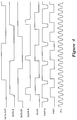
- Figure 4 illustrates a timing diagram of the transfer of data from a slow clock domain to a fast clock domain with zero latency introduced into the data path.
- the frequency of clock signal FAST is greater than that of clock signal SLOW.
- the frequency of the clock signal PLL, output from the phase locked loop is four times that of clock signal FAST.
- clock signals FAST and FAST_R are synchronized so that a rising edge of signal FAST_R always precedes a rising edge of signal FAST and a falling edge of FAST_R is much later than a falling edge of FAST.
- SLOW_R has its rising edge a short (albeit variable) period after the rising edge of clock SLOW.
- the falling edge of SLOW_R occurs long before the falling edge of the clock SLOW.
- FIG. 5 illustrates an alternate clock regenerator circuit that has a wide operating range.
- Clock regenerator 500 is formed by phase locked loop 510, doubler 550, divide-by-4 circuit 520, phase advancer 530 and delay line 540.
- Clock signal FAST is provided as input to phase locked loop 510.
- the output of phase locked loop 510 is provided as input to doubler 550.
- the output of doubler 550 is provided as input to divide-by-4 circuit 520 and also provided as a clocking signal to delay line 540.
- the output of divide-by-4 circuit 520 is regenerated clock signal FAST_R.
- Signal FAST_R is also fed back through phase advancer 530 to phase locked loop 510.
- Clock signal SLOW is provided as input to delay line 540, clocks through delay line 540 under control of the frequency doubled output signal from phase locked loop 510 and is output from delay line 540 as regenerated clock signal SLOW_R.
- Phase locked loop 510 operates at a speed equal to twice the speed of clock signal FAST. Because many digital subsystems frequently have a phase locked loop circuit already designed that operates at twice the frequency of the subsystem, it may be the case that phase locked loop 510 can be implemented using a circuit that has already been designed without the need to introduce new frequency limits as may be the case for a phase locked loop that operates at four times the frequency of the subsystem. The output of phase locked loop 510 is then doubled in frequency by doubler 550 to a speed equal to four times the speed of clock signal FAST. Divide-by-4 circuit 520 is a one-shot clear circuit that operates off of the output signal from doubler 550.
- phase advancer 530 inserts a slight phase advance to the signal output from divide-by-4 circuit 520.
- the purpose of the slight phase advance is to compensate for any jitter in clock signal FAST or introduced by phase locked loop 510.
- regenerated clock signal FAST_R output from divide-by-4 circuit 520 has approximately the same frequency as clock signal FAST.
- clock signal FAST has a duty cycle of fifty percent
- clock signal FAST_R has a duty signal of twenty-five percent.
- clock signals FAST and FAST_R are synchronized so that a rising edge of signal FAST_R always precedes a rising edge of signal FAST and a falling edge of FAST_R will be much later than a falling edge of FAST. Therefore, it is clear from these constraints that the output flip flop 220 will function without a problem.
- Delay line 540 is a one-shot delay line with an asynchronous clear.
- the SLOW clock is regenerated by passing it through delay line 540.
- the delay of delay line 540 is just greater than an integer multiple (e.g. 1, 2, 3, etc.) of a SLOW clock period.
- the length of the delay line may be programmed in hardware, in software or self-programmed.
- the clock signal SLOW is input to delay line 540 and clocks through delay line 540 under the control of the frequency doubled output signal from phase locked loop 510.
- the output of delay line 540 is regenerated clock signal SLOW_R
- Delay line 540 has an asynchronous one-shot clear mechanism to create a reduced duty cycle on SLOW_R the delay line asynchronously clears to '0' after passing a '1' out.
- signal SLOW_R transitions from low to high
- regenerated clock signal SLOW_R will asynchronously transition from high to low before the next phase locked loop clock.
- delay line 540 By making the output of delay line 540 be a short pulse controlled by a separate monostable circuit, a wider operating range is permitted than is the case where the reset is tied to the output of phase locked loop 510.
- the asynchronous reset ensures good compatibility between clocks SLOW and SLOW_R while removing the limitation that the period of phase locked loop 510 be less than half of one phase of clock SLOW.
- clock regenerator 500 will function properly even when the frequency of the clock herein referred to as SLOW is slightly greater than the frequency of the clock herein referred to as FAST.
- Delay line 540 inserts a metastability settling delay into the clock path.
- any metastability between the slow and fast clock domains will occur at the start of delay line 540 and will have the whole length of delay line 540 to settle out (i.e. 1, 2 or 3 cycles of a slow clock period).
- SLOW_R has its rising edge a short (albeit variable) period after the rising edge of clock SLOW.
- the falling edge of SLOW_R occurs long before the falling edge of the clock SLOW. Therefore it is clear that the input flip flop will work without problem.
- SLOW_R and FAST_R are created from the same source (i.e. phase locked loop 510), the intermediate data transfer from the input flip flop to the output flip flop 220 will work without problem.
- FIG. 6 illustrates a self-programming digital delay line suitable for use in a synchronizer wherein the relative speeds of the clock domains is not known a priori.
- Self-programming delay line 600 is formed by flip flops 602, 604 and 606, phase frequency detector 640, up/down counter 610, OR gate 630 and by AND gates 622, 624 and 626.
- Clock signal SLOW is provided as input to a delay line formed by coupling flip flops 602, 604 and 606 in series.
- the phase locked loop generated clock signal PLL_CLOCK controls flip flops 602, 604 and 606, and hence the propagation of clock signal SLOW through the delay line.
- the output from flip flop 606, i.e. the final flip flop in the delay line, is fed back to reset flip flops 602 and 604, thereby providing a one-shot synchronous reset mechanism for self-programming delay line 600.
- phase frequency detector 640 The clock signal SLOW and the output of flip flop 606 are provided as input to phase frequency detector 640.
- Phase frequency detector compares its two inputs and, depending upon their relative values, provides signal UP or DOWN to up/down counter 610.
- Up/down counter 610 is formed by registers 612, 614 and 616 which correspond to flip flops 602, 604 and 606, respectively.
- the output of flip flop 602 and the output of its corresponding register 612 of up/down counter 610 are coupled together by AND gate 622.
- the output of flip flop 604 and the output of its corresponding register 614 of up/down counter 610 are coupled together by AND gate 624.
- OR gate 630 the output of OR gate 630, in turn, is the regenerated clock signal SLOW_R.
- the flip flop of the delay line that provides signal SLOW_R as output is determined by the particular register of up/down counter 610 that has been set.
- the particular register of up/down counter 610 that has been set is determined by a comparison made by phase frequency detector 640 of clock signal SLOW and the output of the final flip flop of the delay line (which is controlled by signal PLL_CLOCK that was generated from clock signal FAST). Therefore, self-programming delay line 600 will automatically adjust the metastability settling delay that it provides to regenerated clock signal SLOW_R based upon the relative frequencies of clock signals SLOW and FAST to provide the proper delay.
- the synchronizer circuit presented herein can be applied, for example, to synchronize a processor to a bus.
- clock FAST would be the clock of the processor and clock SLOW would be the clock of the bus.
- Data from the processor then would be that of signal DATA IN and data to the bus would be that of signal DATA OUT.
- clock FAST would be the clock of the bus and clock SLOW would be the clock of the processor.
- Data from the bus then would be that of signal DATA IN and data to the processor would be that of signal DATA OUT.
- clock FAST would be the clock of the bus and clock SLOW would be the clock of the processor.
- Data from the bus then would be that of signal DATA IN and data to the processor would be that of signal DATA OUT.
Landscapes
- Engineering & Computer Science (AREA)
- Theoretical Computer Science (AREA)
- Computer Networks & Wireless Communication (AREA)
- Signal Processing (AREA)
- Physics & Mathematics (AREA)
- General Engineering & Computer Science (AREA)
- General Physics & Mathematics (AREA)
- Synchronisation In Digital Transmission Systems (AREA)
- Information Transfer Systems (AREA)
Applications Claiming Priority (2)
| Application Number | Priority Date | Filing Date | Title |
|---|---|---|---|
| US08/230,489 US5548620A (en) | 1994-04-20 | 1994-04-20 | Zero latency synchronized method and apparatus for system having at least two clock domains |
| US230489 | 1994-04-20 |
Publications (2)
| Publication Number | Publication Date |
|---|---|
| EP0678990A2 true EP0678990A2 (de) | 1995-10-25 |
| EP0678990A3 EP0678990A3 (de) | 1998-04-22 |
Family
ID=22865428
Family Applications (1)
| Application Number | Title | Priority Date | Filing Date |
|---|---|---|---|
| EP95302556A Withdrawn EP0678990A3 (de) | 1994-04-20 | 1995-04-18 | Synchronisiereinrichtung und -verfahren ohne Latenz für System mit mindestens zwei Taktgebern |
Country Status (3)
| Country | Link |
|---|---|
| US (1) | US5548620A (de) |
| EP (1) | EP0678990A3 (de) |
| JP (1) | JPH0855084A (de) |
Cited By (8)
| Publication number | Priority date | Publication date | Assignee | Title |
|---|---|---|---|---|
| WO1999019786A1 (en) * | 1997-10-10 | 1999-04-22 | Micron Technology, Inc. | Method and apparatus for coupling signals between two circuits operating in different clock domains |
| WO1999019785A1 (en) * | 1997-10-10 | 1999-04-22 | Rambus Incorporated | Apparatus and method for generating a distributed clock signal using gear ratio techniques |
| WO2000008544A1 (en) * | 1998-08-04 | 2000-02-17 | Juniper Networks | Synchronizing data transfers between two distinct clock domains |
| WO2000010354A1 (en) * | 1998-08-14 | 2000-02-24 | Qualcomm Incorporated | Synchronisation of a low power clock in a wireless communication device |
| US6434684B1 (en) | 1998-09-03 | 2002-08-13 | Micron Technology, Inc. | Method and apparatus for coupling signals across different clock domains, and memory device and computer system using same |
| US7568118B2 (en) * | 2005-09-20 | 2009-07-28 | Intel Corporation | Deterministic operation of an input/output interface |
| FR2996968A1 (fr) * | 2012-10-11 | 2014-04-18 | St Microelectronics Sa | Circuit de protection de rapport cyclique |
| EP4191884A1 (de) * | 2021-12-01 | 2023-06-07 | Nxp B.V. | Synchronisierschaltung |
Families Citing this family (41)
| Publication number | Priority date | Publication date | Assignee | Title |
|---|---|---|---|---|
| US6169772B1 (en) * | 1995-04-07 | 2001-01-02 | Via-Cyrix, Inc. | Stretching setup and hold times in synchronous designs |
| WO1997006491A1 (en) * | 1995-08-10 | 1997-02-20 | International Business Machines Corporation | Synchronizing logic avoiding metastability |
| US5831459A (en) * | 1995-11-13 | 1998-11-03 | International Business Machines Corporation | Method and system for adjusting a clock signal within electronic circuitry |
| JP2914267B2 (ja) * | 1996-01-30 | 1999-06-28 | 日本電気株式会社 | 集積回路のデータ転送方法およびその装置 |
| US5905766A (en) * | 1996-03-29 | 1999-05-18 | Fore Systems, Inc. | Synchronizer, method and system for transferring data |
| JP3000961B2 (ja) | 1997-06-06 | 2000-01-17 | 日本電気株式会社 | 半導体集積回路 |
| KR100477327B1 (ko) * | 1997-06-11 | 2005-07-07 | 삼성전자주식회사 | 동기디램용다이나믹클럭발생회로 |
| DE19737589C1 (de) * | 1997-08-28 | 1998-11-26 | Siemens Ag | Interfaceschaltung für fullcustom- und semicustom-Taktdomänen |
| US6233656B1 (en) * | 1997-12-22 | 2001-05-15 | Lsi Logic Corporation | Bandwidth optimization cache |
| US6097775A (en) * | 1998-02-17 | 2000-08-01 | Lsi Logic Corporation | Method and apparatus for synchronously transferring signals between clock domains |
| US6014708A (en) * | 1998-02-19 | 2000-01-11 | Alcatel | Adaptor and method for mapping a fast ethernet payload input signal to a synchronous payload envelope, as well as a clock selector for use therewith |
| JPH11265313A (ja) * | 1998-03-18 | 1999-09-28 | Hitachi Ltd | 記憶装置 |
| US6549593B1 (en) | 1999-07-19 | 2003-04-15 | Thomson Licensing S.A. | Interface apparatus for interfacing data to a plurality of different clock domains |
| US6895061B1 (en) * | 1999-10-26 | 2005-05-17 | Agilent Technologies, Inc. | Scannable synchronizer having a deceased resolving time |
| US6928574B1 (en) * | 2001-08-23 | 2005-08-09 | Hewlett-Packard Development Company, L.P. | System and method for transferring data from a lower frequency clock domain to a higher frequency clock domain |
| US6931562B1 (en) * | 2001-08-23 | 2005-08-16 | Hewlett-Packard Development Company, L.P. | System and method for transferring data from a higher frequency clock domain to a lower frequency clock domain |
| DE10152195A1 (de) * | 2001-10-23 | 2003-04-30 | Koninkl Philips Electronics Nv | Schaltungsanordnung |
| US6959398B2 (en) * | 2001-12-31 | 2005-10-25 | Hewlett-Packard Development Company, L.P. | Universal asynchronous boundary module |
| US6839391B2 (en) * | 2002-01-08 | 2005-01-04 | Motorola, Inc. | Method and apparatus for a redundant clock |
| US6777989B2 (en) | 2002-05-07 | 2004-08-17 | The Boeing Company | Generation of synchronized clocks to multiple locations in a system |
| US6954869B2 (en) * | 2002-09-26 | 2005-10-11 | Analog Devices, Inc. | Methods and apparatus for clock domain conversion in digital processing systems |
| DE10255685B3 (de) * | 2002-11-28 | 2004-07-29 | Infineon Technologies Ag | Taktsynchronisationsschaltung |
| US20040193931A1 (en) * | 2003-03-26 | 2004-09-30 | Akkerman Ryan L. | System and method for transferring data from a first clock domain to a second clock domain |
| US6900665B2 (en) * | 2003-06-10 | 2005-05-31 | James Ma | Transfer of digital data across asynchronous clock domains |
| US6906555B2 (en) * | 2003-06-10 | 2005-06-14 | James Ma | Prevention of metastability in bistable circuits |
| US7242737B2 (en) | 2003-07-09 | 2007-07-10 | International Business Machines Corporation | System and method for data phase realignment |
| US7639764B2 (en) * | 2005-08-17 | 2009-12-29 | Atmel Corporation | Method and apparatus for synchronizing data between different clock domains in a memory controller |
| US7890684B2 (en) * | 2006-08-31 | 2011-02-15 | Standard Microsystems Corporation | Two-cycle return path clocking |
| US7500132B1 (en) | 2008-04-11 | 2009-03-03 | International Business Machines Corporation | Method of asynchronously transmitting data between clock domains |
| US8132036B2 (en) * | 2008-04-25 | 2012-03-06 | International Business Machines Corporation | Reducing latency in data transfer between asynchronous clock domains |
| US9431091B2 (en) | 2008-06-06 | 2016-08-30 | Uniquify, Inc. | Multiple gating modes and half-frequency dynamic calibration for DDR memory controllers |
| US8866556B2 (en) | 2009-02-27 | 2014-10-21 | Analog Bits, Inc. | Phase shift phase locked loop |
| US20120033772A1 (en) * | 2010-08-08 | 2012-02-09 | Freescale Semiconductor, Inc | Synchroniser circuit and method |
| US8742957B2 (en) | 2010-12-15 | 2014-06-03 | Analog Bits, Inc. | Multi-variable multi-wire interconnect |
| US8848731B2 (en) | 2011-01-31 | 2014-09-30 | Qualcomm Incorporated | System and method for facilitating data transfer using a shared non-deterministic bus |
| US8493108B2 (en) * | 2011-09-16 | 2013-07-23 | Apple Inc. | Synchronizer with high reliability |
| US8937492B1 (en) | 2012-10-24 | 2015-01-20 | Marvell Israel (M.I.S.L) Ltd. | Systems and methods for transferring a signal from a first clock domain to a second clock domain |
| US9020084B2 (en) | 2013-01-31 | 2015-04-28 | Qualcomm Incorporated | High frequency synchronizer |
| US9123408B2 (en) | 2013-05-24 | 2015-09-01 | Qualcomm Incorporated | Low latency synchronization scheme for mesochronous DDR system |
| DE102016107734B4 (de) * | 2016-04-26 | 2024-05-02 | Infineon Technologies Ag | Elektronische Schaltung und Verfahren zur Datenübertragung |
| US12468334B2 (en) * | 2021-07-27 | 2025-11-11 | Synopsys, Inc. | Clock signal realignment for emulation of a circuit design |
Family Cites Families (6)
| Publication number | Priority date | Publication date | Assignee | Title |
|---|---|---|---|---|
| EP0379279A3 (de) * | 1989-01-17 | 1991-09-11 | Marconi Instruments Limited | Datenvermittlungssynchronisator |
| US5008904A (en) * | 1989-07-24 | 1991-04-16 | Hewlett-Packard Co. | Synchronizer using clock phase extrapolation |
| JPH0624356B2 (ja) * | 1989-12-21 | 1994-03-30 | 株式会社東芝 | データ転送方式 |
| JPH0556085A (ja) * | 1991-08-23 | 1993-03-05 | Nec Ic Microcomput Syst Ltd | インターフエイス回路 |
| US5256912A (en) * | 1991-12-19 | 1993-10-26 | Sun Microsystems, Inc. | Synchronizer apparatus for system having at least two clock domains |
| US5422914A (en) * | 1993-09-07 | 1995-06-06 | Motorola, Inc. | System and method for synchronizing data communications between two devices operating at different clock frequencies |
-
1994
- 1994-04-20 US US08/230,489 patent/US5548620A/en not_active Expired - Lifetime
-
1995
- 1995-04-18 EP EP95302556A patent/EP0678990A3/de not_active Withdrawn
- 1995-04-20 JP JP7117713A patent/JPH0855084A/ja active Pending
Cited By (16)
| Publication number | Priority date | Publication date | Assignee | Title |
|---|---|---|---|---|
| US6396887B1 (en) | 1997-10-10 | 2002-05-28 | Rambus Incorporated | Apparatus and method for generating a distributed clock signal using gear ratio techniques |
| WO1999019785A1 (en) * | 1997-10-10 | 1999-04-22 | Rambus Incorporated | Apparatus and method for generating a distributed clock signal using gear ratio techniques |
| US6000022A (en) * | 1997-10-10 | 1999-12-07 | Micron Technology, Inc. | Method and apparatus for coupling signals between two circuits operating in different clock domains |
| WO1999019786A1 (en) * | 1997-10-10 | 1999-04-22 | Micron Technology, Inc. | Method and apparatus for coupling signals between two circuits operating in different clock domains |
| US7263149B2 (en) | 1997-10-10 | 2007-08-28 | Rambus Inc. | Apparatus and method for generating a distributed clock signal |
| US6366991B1 (en) | 1997-10-10 | 2002-04-02 | Micron Technology, Inc. | Method and apparatus for coupling signals between two circuits operating in different clock domains |
| WO2000008544A1 (en) * | 1998-08-04 | 2000-02-17 | Juniper Networks | Synchronizing data transfers between two distinct clock domains |
| US6359479B1 (en) | 1998-08-04 | 2002-03-19 | Juniper Networks, Inc. | Synchronizing data transfers between two distinct clock domains |
| WO2000010354A1 (en) * | 1998-08-14 | 2000-02-24 | Qualcomm Incorporated | Synchronisation of a low power clock in a wireless communication device |
| US6333939B1 (en) | 1998-08-14 | 2001-12-25 | Qualcomm Incorporated | Synchronization of a low power oscillator with a reference oscillator in a wireless communication device utilizing slotted paging |
| US6434684B1 (en) | 1998-09-03 | 2002-08-13 | Micron Technology, Inc. | Method and apparatus for coupling signals across different clock domains, and memory device and computer system using same |
| US6775755B2 (en) | 1998-09-03 | 2004-08-10 | Micron Technology, Inc. | Method and apparatus for coupling signals across different clock domains, and memory device and computer system using same |
| US7568118B2 (en) * | 2005-09-20 | 2009-07-28 | Intel Corporation | Deterministic operation of an input/output interface |
| FR2996968A1 (fr) * | 2012-10-11 | 2014-04-18 | St Microelectronics Sa | Circuit de protection de rapport cyclique |
| US9197197B2 (en) | 2012-10-11 | 2015-11-24 | Stmicroelectronics Sa | Duty cycle protection circuit |
| EP4191884A1 (de) * | 2021-12-01 | 2023-06-07 | Nxp B.V. | Synchronisierschaltung |
Also Published As
| Publication number | Publication date |
|---|---|
| US5548620A (en) | 1996-08-20 |
| JPH0855084A (ja) | 1996-02-27 |
| EP0678990A3 (de) | 1998-04-22 |
Similar Documents
| Publication | Publication Date | Title |
|---|---|---|
| US5548620A (en) | Zero latency synchronized method and apparatus for system having at least two clock domains | |
| JP2610213B2 (ja) | 同期装置及び同期方法 | |
| US5535377A (en) | Method and apparatus for low latency synchronization of signals having different clock speeds | |
| EP0208449B1 (de) | Gerät zur Synchronisation eines ersten Signals mit einem zweiten Signal | |
| EP1262022B1 (de) | Verfahren und Schaltungsanordung zur Datenübertragung zwischen pseudo-synchronisierten Kanälen | |
| US7239681B2 (en) | System and method for maintaining a stable synchronization state in a programmable clock synchronizer | |
| JP3565600B2 (ja) | データ通信装置およびデータ通信方法 | |
| US4405898A (en) | Pseudo synchronous clocking | |
| US5808571A (en) | Synchronization control unit which maintains synchronization between serial-to-parallel converters operating in parallel, or between parallel-to-serial converters operating in parallel | |
| US5919265A (en) | Source synchronization data transfers without resynchronization penalty | |
| EP0677802A1 (de) | Vorrichtung und Verfahren zur Erzeugung eines phasengesteuerten Taktsignals | |
| US4811364A (en) | Method and apparatus for stabilized data transmission | |
| KR100195855B1 (ko) | 소수배 시스템에 있어서 클록 동기 체계 | |
| US20020196886A1 (en) | SYNC pulse compensation and regeneration in a clock synchronizer controller | |
| US5634116A (en) | Non-integer multiple clock translator | |
| US20040193931A1 (en) | System and method for transferring data from a first clock domain to a second clock domain | |
| JPH10222243A (ja) | データ転送の間にサブシステム・クロックに一時的に同期される自由走行クロックを有するプロセッサを含むシステム | |
| EP1157465A1 (de) | Verfahren und vorrichtung zur störimpulsfreien auswahl eines taktsignales | |
| US5008904A (en) | Synchronizer using clock phase extrapolation | |
| US7333516B1 (en) | Interface for synchronous data transfer between domains clocked at different frequencies | |
| US4823365A (en) | Synchronization method and elastic buffer circuit | |
| EP0319184B1 (de) | Zweistufige Synchronisiereinrichtung | |
| US6956918B2 (en) | Method for bi-directional data synchronization between different clock frequencies | |
| US6928574B1 (en) | System and method for transferring data from a lower frequency clock domain to a higher frequency clock domain | |
| US6577649B1 (en) | Multiplexer for asynchronous data |
Legal Events
| Date | Code | Title | Description |
|---|---|---|---|
| PUAI | Public reference made under article 153(3) epc to a published international application that has entered the european phase |
Free format text: ORIGINAL CODE: 0009012 |
|
| AK | Designated contracting states |
Kind code of ref document: A2 Designated state(s): DE FR GB NL SE |
|
| PUAL | Search report despatched |
Free format text: ORIGINAL CODE: 0009013 |
|
| AK | Designated contracting states |
Kind code of ref document: A3 Designated state(s): DE FR GB NL SE |
|
| 17P | Request for examination filed |
Effective date: 19981012 |
|
| 17Q | First examination report despatched |
Effective date: 20030123 |
|
| GRAP | Despatch of communication of intention to grant a patent |
Free format text: ORIGINAL CODE: EPIDOSNIGR1 |
|
| STAA | Information on the status of an ep patent application or granted ep patent |
Free format text: STATUS: THE APPLICATION IS DEEMED TO BE WITHDRAWN |
|
| 18D | Application deemed to be withdrawn |
Effective date: 20041103 |