EP0680210B1 - Système de conversion de base de temps - Google Patents
Système de conversion de base de temps Download PDFInfo
- Publication number
- EP0680210B1 EP0680210B1 EP95302840A EP95302840A EP0680210B1 EP 0680210 B1 EP0680210 B1 EP 0680210B1 EP 95302840 A EP95302840 A EP 95302840A EP 95302840 A EP95302840 A EP 95302840A EP 0680210 B1 EP0680210 B1 EP 0680210B1
- Authority
- EP
- European Patent Office
- Prior art keywords
- time
- clock
- base
- conversion system
- signal
- Prior art date
- Legal status (The legal status is an assumption and is not a legal conclusion. Google has not performed a legal analysis and makes no representation as to the accuracy of the status listed.)
- Expired - Lifetime
Links
- 238000006243 chemical reaction Methods 0.000 title claims description 55
- 230000006835 compression Effects 0.000 claims description 68
- 238000007906 compression Methods 0.000 claims description 68
- 230000015654 memory Effects 0.000 claims description 40
- 230000009977 dual effect Effects 0.000 claims description 5
- 239000004065 semiconductor Substances 0.000 claims description 3
- 238000010586 diagram Methods 0.000 description 30
- 238000011045 prefiltration Methods 0.000 description 15
- 238000010276 construction Methods 0.000 description 10
- 238000005070 sampling Methods 0.000 description 10
- 230000004048 modification Effects 0.000 description 3
- 238000012986 modification Methods 0.000 description 3
- 230000008859 change Effects 0.000 description 2
- 230000007257 malfunction Effects 0.000 description 2
- 239000011159 matrix material Substances 0.000 description 2
- 238000004891 communication Methods 0.000 description 1
- 230000007423 decrease Effects 0.000 description 1
- 230000003247 decreasing effect Effects 0.000 description 1
- 238000001914 filtration Methods 0.000 description 1
- 230000006870 function Effects 0.000 description 1
- 230000007274 generation of a signal involved in cell-cell signaling Effects 0.000 description 1
- 239000000463 material Substances 0.000 description 1
- 238000000034 method Methods 0.000 description 1
- 230000008569 process Effects 0.000 description 1
- 230000004044 response Effects 0.000 description 1
Images



Classifications
-
- H—ELECTRICITY
- H04—ELECTRIC COMMUNICATION TECHNIQUE
- H04N—PICTORIAL COMMUNICATION, e.g. TELEVISION
- H04N11/00—Colour television systems
-
- H—ELECTRICITY
- H04—ELECTRIC COMMUNICATION TECHNIQUE
- H04N—PICTORIAL COMMUNICATION, e.g. TELEVISION
- H04N7/00—Television systems
- H04N7/01—Conversion of standards, e.g. involving analogue television standards or digital television standards processed at pixel level
- H04N7/0135—Conversion of standards, e.g. involving analogue television standards or digital television standards processed at pixel level involving interpolation processes
-
- H—ELECTRICITY
- H04—ELECTRIC COMMUNICATION TECHNIQUE
- H04N—PICTORIAL COMMUNICATION, e.g. TELEVISION
- H04N5/00—Details of television systems
- H04N5/14—Picture signal circuitry for video frequency region
-
- H—ELECTRICITY
- H04—ELECTRIC COMMUNICATION TECHNIQUE
- H04N—PICTORIAL COMMUNICATION, e.g. TELEVISION
- H04N7/00—Television systems
- H04N7/01—Conversion of standards, e.g. involving analogue television standards or digital television standards processed at pixel level
- H04N7/0117—Conversion of standards, e.g. involving analogue television standards or digital television standards processed at pixel level involving conversion of the spatial resolution of the incoming video signal
- H04N7/0122—Conversion of standards, e.g. involving analogue television standards or digital television standards processed at pixel level involving conversion of the spatial resolution of the incoming video signal the input and the output signals having different aspect ratios
Definitions
- the present invention relates generally to a time-base conversion system suitable for use in television receivers. information communication equipments and the like, and more particularly to a a time-base converter such as a time-base compressor, a time-base expander and the like and its applications.
- a time-base converter such as a time-base compressor, a time-base expander and the like and its applications.
- Such time-base conversion systems are described for example in US-A-4 691248 or in IEEE Transactions on Consumer Electronics, Vol. 38, no 3, 08/92, New York, US, p. 303 - 311.
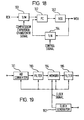
- FIGURE 19 shows an example of a time-base compressor in conventional time-base conversion systems.
- this example of the time-base compressor is constructed to compress the time-base by conducting a thinning operation of signal data to be written into a memory by a digital filter and by reading the signal.
- a compression ratio of the time-base is determined by a thinning ratio for thinning data to be written into a memory.
- the input analog signals are converted into digital signals having a prescribed sampling period based on the clock frequency by an AD converter 191.
- the clock signal is generated as a clock having a prescribed period by a clock signal generator 192.
- the converted digital signal data are thinned out by a digital filter 193 on the time-base in order to determine a required compression ratio, for instance, to compress the data to 3/4 times.
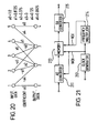
- An FIR type filter is often used for this digital filter 193. For the thinning operation, it is necessary to properly determine tap coefficiente in order to take three signal data out of four different signal data continuous on the time-base. Examples of the tap coefficients are shown in FIGURE 20.
- the signal data thinned out on the time-base are written into a memory 194.
- the written signal data are read out in the same period as a prescribed sampling period according to the clock frequency of the clock generator 192 and the read digital signal data are converted into analog signals by an AD converter 195.
- the converted analog signals become to a compressed data that the input analog signal are compressed on a 3/4 times time-base. Thus, the time-base is compressed.
- the digital filter 193 is used for thinning the time-base to compress the time-base.
- a filter comprising a digital circuit is increased its size and complicated in the circuit arrangement and often causes a bottleneck in achieving a system. Further, when making a circuit scale small, it becomes difficult to achieve a desired performance.
- filters such as FIR type filters are used for the time-base thinning operation and there is a problem that a circuit scale becomes large and the circuit arrangement is complicated. If tried to make a circuit scale small in this construction, it is difficult to achieve a desired performance.
- FIGURE 21 shows another example of conventional time-base compressors for solving the problems as described above.
- This is a time-base compressor constructed to achieve the time-base compression by making the memory write clock frequency and read clock frequency different each other by means of compressing time-bases of input and output signals.
- a read clock is generated by multiplying a write clock, and a time-base compression ratio is fixed by determining a multiplication ratio.
- Input analog signals are converted into digital signals having a prescribed sampling period based on the write clock frequency.
- This write clock is generated as a clock having a prescribed period by a clock generator 212.
- the converted digital signals are written into a memory 213 based on the write clock.
- a read clock is generated by multiplying the write clock generated in the clock generator 212 by a multiplier 214 with a 4/3 times multiplication ratio. This multiplying operation is performed by using, for instance, a PLL.
- the signal data written into the memory by the write clock are read based on the read clock.
- the read digital signal data are converted into analog signals by a DA converter 215.
- the converted output analog signals are turned to data that are obtained by compressing input analog signals on the 3/4 times time-base through the signal processing described above. The time-base compression can be thus performed,
- time-base compressor it is not required to use a digital filter for the time-base thinning to perform the time-base compression. Therefore, the circuit construction is made simple and it becomes more easy to achieve a system than the conventional apparatus described above.
- the time-base is compressed corresponding to a multiplication ratio of the write clock based on the write clock to the memory 213, there is such a problem that the read clock frequency increases by a multiple of compression ratio. That is, as the read clock will be increased corresponding to a compression ratio if the compression ratio increases, the access speed to the memory 213 or the operating speed of the AD converter 215 excedes its upper limit and as a result, it becomes difficult to achieve the time-base conversion system.
- the conventional time-base conversion system has such a problem that one clock jitter occurs between the write clock and the read clock, and a reproduced video pictuer with a satisfactory quality cannot be obtained in a system where read and write clock frequencies are different each other.
- the system which generates a read clock and a write clock based on a horizontal synch, signal and converts a wide aspect ratio by keeping the read clock frequency constant and varying the write clock frequency, and applying a filter selecting signal corresponding to a compression ratio. selects a filter of the optimum frequency band for the system corresponding to the change in the write sampling frequency.
- the VCO (Voltage Control Oscillator) system in which a write clock generating VCO operates based on a clock generated by a read clock generating VCO and a read timing generating counter which is operated by a read clock a write timing generating counter which is operated by a write clock are cleared by a clear signal generated by the read clock or the write clock at every line (for instance, 1824 times period of a read clock period) because of a difference between the read clock frequency and the write clock frequency.
- a frequency divider which converts the VCO output for generating a write clock to a signal for phase comparison with a read clock is provided with a control signal input that is externally controllable and its frequency division is variable as desired by an external control signal supplied from the outside.
- the time-base is converted by changing a write clock based on a read clock of a memory, the circuit scale can be made small and even when a compression ratio is made large, a read clock frequency is kept constant and a large compression ratio can be easily achieved.
- a write frequency is high, a wide frequency band filter is selected and if it is low, a narrow frequency band filter is selected for preventing the aliasing error and as the optimum filter is selected corresponding to a compression ratio, reproduced video in high quality of picture can be always obtained.
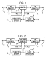
- FIGURE 1 illustrates a system for explaining one embodiment of the present invention.
- this is a time-base compressor constructed to perform a time-base compression by making the write clock frequency and the read clock frequency to and from a memory different with each other.
- a write clock is generated by dividing a read clock and a compression ratio of the time-base is determined by determining a frequency dividing ratio based on the read clock.
- An analog signals input to an input terminal 1 is converted into a digital signal with a prescribed sampling period by an AD converter 2 based on a write clock frequency.
- This write clock is generated by dividing a read clock in a frequency divider 3 at a prescribed frequency division ratio, for instance, by a 3/4 times frequency divider. This frequency division is performed using, for instance, a programmable frequency divider.
- the converted digital signals are written into a memory 4 based on the write clock.
- a read clock is generated by a clock generator 5.
- the signal data written into a memory based on a write clock are read based on the read clock, and the read digital signal data are converted into analog signals by a DA converter 6.
- the converted output analog signals are led out from an output terminal 7 as the input analog signal data compressed on a 3/4 times time-base.
- the time base compression can be achieved in the process described above.
- a digital filter for thinning a timebase for the time-base compression is not used. Therefore, the circuit configuration becomes simple and it is easy to achieve the circuit as the time-base conversion system. Furthermore, as the time-base is compressed by dividing a read clock at a frequency dividing ratio determined based on a read clock of the memory 4, this circuit has a feature that the write clock frequency is lowered by a multiple of compression ratio. Thus, even when a large compression ratio is used, a read clock is not increased higher in proportion to the compression ratio but a write clock is rather lowered. and therefore it is easy to achieve this system without being subject to restriction by an access speed to the memory 4 and the operating speed of the DA converter 6.
- FIGURE 2 is a diagram showing the circuit construction.
- the time-base compressor of this embodiment is constructed to perform the time-base compression by making the memory write clock frequency different from the read clock frequency by means of compressing the time-base of input and output signals.
- This embodiment differs from the embodiment shown in FIGURE 1 in that a dual port memory 41 is used.
- a write clock is generated by dividing a read clock, and a time-base compression ratio is determined by determining a frequency dividing ratio based on the read clock.
- Input analog signals are converted into digital signals having a prescribed sampling period corresponding to the write clock frequency by the AD converter 2.
- This write clock is generated as a clock by dividing a read clock in a frequency dividing circuit 3 at a prescribed dividing ratio, for instance, 3/4 times division.
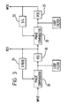
- FIGURES 3 and 4 are both for explaining the definite circuit diagrams of the frequency divider 3 and the read clock generator 5 in the PLL configuration which are used in FIGURES 1 and 2.
- a write clock is generated by a VCO 31 and after dividing the write clock by a 4/3 times frequency divider 32, it is input into a phase comparator 33 and a read clock is input into the phase comparator 33 and the output of the phase comparator 33 is made as a control voltage of the VCO 31.
- a PLL circuit is thus constructed.
- a read clock is generated by a PLL circuit which is comprised of a frequency divider 34 to achieve 1820 times a television horizontal synchronizing timing equivalent to the 8 fsc, a comparator 35 and a VCO 36.
- a write clock is generated from a VCO 41 and after dividing it in a 1/3 times frequency divider 42, the divided write clock is input into a phase comparator 43, and dividing a read clock to 1/4 times by 1/2 times frequency dividers 44, 45, the divided read clocks is input into the phase comparator 43 and the output of the phase comparator 43 is used as a control voltage of the VCO 31.
- the PLL circuit is thus constructed.
- the read clock is generated by the PLL circuit which is comprised of 1/2 times frequency dividers 44, 46 to multiply a television horizontal timing by 1820 equivalent to 8 fsc, a comparator 47 and a VCO 48.
- the frequency divider to obtain 1820 times is in such a structure that a part or all of the 1/4 times frequency divider is applied.
- a result that. is obtained by a circuit in any construction is that a write clock in frequency resulting from multiplying a read clock by 3/4 times can be obtained.
- the converted digital signals are written into the memory 41 based on the write clock.
- the read clock reads signal data written based on the write clock, which is generated by the clock generator 5. based on the read clock and converts the read digital signal data into analog signals by the DA converter 6.
- the converted output analog signals are led out from the output terminal 7 as input analog signal data compressed on the 3/4 times time-base.
- a digital filter for thinning out the time-base i.e., for performing the time-base compression is also not needed likewise the embodiment shown in FIGURE 1.
- the circuit configuration becomes more simple and it is easy to achieve a time-base compression system.
- the time-base is compressed by dividing a read clock according to a frequency dividing ratio determined based on the read clock from the memory 41, this embodiment has a feature that the write clock frequency is decreased by a multiple of compression ratio likewise the embodiment shown in FIGURE 1. Even when a large compression ratio is used, the read clock does not increase in proportion to a compression ratio but rather the write clock decreases. It is therefore easy to achieve a circuit without constraints of the access speed to the memory 41 and the operational speed of the DA converter 6,
- FIGURE 5 is a system diagram with the time-base compressor described in FIGURE 2 applied to luminance signal and chrominance signal processing systems of a practical television receiver. Further, in this block diagram a voice signal processor was omitted.
- Television carrier signals received by a tuner 51 are demodulated by a demodulator 52 and separated into luminance signals and chrominance signals by a luminance signal/chrominance signal separator 53.
- luminance signals and the chrominance signals are processed as baseband video signals in a luminance signal processor 54 and a chrominance signal processor 55, respectively, they are input to a time-base compressor 56.
- the luminance signals and the chrominance signals are processed for the time-base compression independently.
- the luminance and chrominance signals are multiplied by 3/4 so that a 4 : 3 aspect picture frame can be displayed on a 16 : 9 aspect screen at a proper aspect ratio.
- the compressed baseband luminance signals and chrominance signals are converted into RGB signals by a matrix unit 57 and displayed as a picture frame on a CRT 59 via a deflector 58.
- the picture frame at this time is a picture frame which was compressed by 3/4 times in the clockwise direction by the time-base compressor 56.
- the width of a 16 : 9 aspect television receiver is longer than a 4 : 3 aspect television receiver by 4/3 times, the aspect ratio can be reproduced precisely.
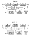
- FIGURE 6 is a circuit diagram for explaining the second embodiment of the present invention.
- the circuit of this embodiment is a time-base expander which expands the time-base of input and output signals by making the write clock frequency and the read clock frequency for memories different with each other.
- a write clock is generated by multiplying a read clock at an expansion ratio of the time-base by determining a multiplication ratio based on the read clock.
- analog signals input to the input terminal 1 are converted into digital signals having a prescribed sampling period corresponding to the write clock frequency by the AD converter 2.
- This write clock is generated by multiplying a read clock by 4/3 times at a multiplier 61. This multiplication is carried out using a programmable multiplier.
- the converted digital signals are written into the memory 4 based on the write clock.
- the read clock is generated by the clock generator 5.
- the signal data written based on the write clock are read based on the read clock and the read digital signal data are converted into analog signals by the DA converter 6.
- the converted output analog signals become data that are obtained by expanding input analog signal data on a 4/3 times time-base.
- the expaneion of the time-base is thus executed.
- this time-base expander no digital filter is required for the time-base thinning for performing the time-base compression. Therefore, the entire circuit configuration becomes simple and it becomes possible to make the circuit as a time-base conversion system that can be achieved.
- FIGURE 7 is a circuit diagram for explaining the third embodiment of the present invention.
- This embodiment relates to a time-base expander which expands a time-base of input and output signals by differentiating the write clock frequency from the read clock frequency.
- the circuit shown in FIGURE 7 differs from the second embodiment shown in FIGURE 6 in that this circuit uses the dual port type semiconductor memory 41.
- a time-base expansion ratio is determined by generating a write clock by multiplying a read clock and a time-base expansion ratio is determined based on the read clock.
- analog signals input to the input terminal 1 are converted into digital signals having a prescribed sampling period corresponding to the write clock frequency by the AD converter 2.
- This write clock is generated as a clock resulting from multiplying the read clock by 4/3 times in the multiplier 61.
- a PLL circuit is used for this multiplier 6, for instance.
- the converted digital signals are written into the memory based on the write clock.
- a read clock is generated by a clock generator.
- the signal data written into a memory by the write clock are read and the read digital signal data are converted into analog signals by the DA converter.
- the converted output analog signals become data that are the input analog signals expanded on a 4/3 times time-base. The time-base expansion is thus executed.
- a digital filter is also not required for the time-base thinning in performing the time-base expansion likewise the embodiment shown in FIGURE 6. Further, it is possible to make the circuit configuration more simple as the dual port memory 41 is used.
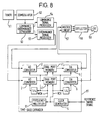
- FIGURE 8 shows a system diagram with the time-base expander explained in FIGURE 6 applied to luminance signal and chrominance signal processing systems of a practical television receiver, independently.
- a voice signal processor was omitted.
- the television carrier signals received by the tuner 51 are separated into luminance signals and chrominance signals by the luminance signal/chrominance signal separator 53 after demodulated by the demodulator 52.
- the luminance and chrominance signals are processed to baseband video signals by the luminance signal processor 54 and the chrominance signal processor 55, respectively and then input to a time-base expander 81.
- the luminance signals and chrominance signals are processed independently for the time-base expansion. In the time-base expander 81, they are multiplied by 4/3 times so that a 16 : 9 aspect picture frame is displayed on a 4 : 3 aspect screen at a proper aspect ratio.
- the expanded baseband luminance signals and the baseband chrominance signals are converted into RGB signals by the matrix unit 57 and displayed as a picture frame on the CRT 59 via the deflector 58.
- the picture frame at this time is that expanded by 4/3 times in the clockwise direction by the time-base expander 81.
- the aspect ratio can be reproduced precisely as the width of the screen of a 4 : 3 aspect television receiver is shorter by 3/4 times than a 16 : 9 aspect television receiver.
- a clock that is an integer times of horizontal synch, signal of video signal is normally used as it is necessary to arrange the aspect converted video signal data in the vertical direction. It is therefore necessary to match the clock to the clock system of the entire system in some form.
- the aspect converted clock frequency is widely differing from the clock frequency of the entire system, it becomes very difficult to obtain the matching of the entire system.
- the color lock clock has been set at 455/2 times of the horizontal synch, signal and it would be 1820 times if 8 times clock of it was used.
- at least aspect conversion clock frequency of a value close to 1820 times must be used by taking the system matching into consideration.
- the chrominance signal band is narrower than luminance signal and operates using a clock frequency with 1/4 times that of the luminance signal to reduce a circuit scale.
- the read clock is set at 1824 times the horizontal synch. signal (1824 fH). In this case, it is possible to achieve the 3/4 compression when multiplying the write clock frequency by 3/4 times (1368 fH: luminance signal) and the 1/2 times compression when multiplying the write clock frequency by 1/2 times (912 fH: luminance signal). In the case of the chrominance signal, the compression can be achieved by 1/4 times the clock frequency.
- the read clock frequency is assumed to be, for instance, 30 MHz.
- the 3/4 times compression when the write clock frequency is 22.5 MHz (3/4 times of 30 MHz)
- the 1/2 times compression when the write clock frequency is 15 MHz (1/2 times of 30 MHz)
- no compression when the write clock frequency is 30 MHz.
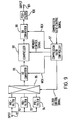
- analog video signals before the aspect conversion are input through an input terminal 91.
- the input analog video signals are input to pre-filters 92 through 94 that are composed of an analog circuit.
- the outputs of the pre-filters 92 through 94 are input to a selector 95.
- the output of the selector 95 is input to an A/D converter 96.
- the A/D converter 96 converts the input analog video signals into digital signals based on the write clock supplied from a compression ratio controller 97.
- the video signals converted into digital signals are input to a compressor 98.
- the compressor 98 is composed of a memory and the like and writes data in the memory by the write clock and reads data from the memory by the read clock supplied from the compression ratio controller 97.
- the aspect converted digital video signals based on the read clock are input to a D/A converter 99.
- the D/A converter 99 reads the digital video signals based on the read clock supplied from the compression ratio controller 97 and converts them into analog video signals.
- the video signals converted into the analog video signals are input to a aliasing error removing post filter 100.
- the video signals with the aliasing error removed by the post filter 100 are aspect converted and output from an output terminal 101.
- a compression ratio control signal is input to the compression ratio controller 97.
- This compression ratio control signal is comprised of, for instance, 2 bits and will be "00" for the 3/4 times compression, "01” for the 1/2 times compression and "10" for no compression.
- the compression ratio controller 97 generates a write clock, read clock and filter control signal according to this compression ratio control signal. At the 3/4 times compression, a write clock of 22.5 MHz frequency and a read clock of 30 MHz frequency are generated.
- the functions of the pre-filters 92 through 94 are to remove aliasing error.
- the frequency band of the pre-filters 92 through 94 must be below the write clock.
- the write clock frequency differs according to the compression modes. Therefore, if this proposal is not used, all modes must be adapted to the most low frequency mode to remove the aliasing error.
- all the pre-filters 92 through 94 in the frequency band below 7.5 MHz, which is a half of the write clock frequency 15 MHz for the 1/2 times compression mode, are to be used in all modes. It is therefore meaningless that high frequencies are used specially to promote the resolution.
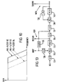
- a pre-filter in the frequency band adapted to the applicable write frequency is selected by a filter control signal that is output from the compression ratio controller 97.
- the characteristics of the pre-filters 92 through 94 having different frequency characteristics are shown in FIGURE 10.
- the pre-filters 92 through 94 are constructed in an analog circuit but they can be constructed in a digital circuit to make the system as a full digital system.
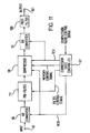
- FIGURE 11 shows the system with the pre-filters constructed in the digital circuit.
- this embodiment differs from that shown in FIGURE 9 in that the pre-filters 92 through 94 and the selector 95 were eliminated and a pre-filter 111 has been connected between the A/D converter 96 and the compressor 98 for filtering digital signals.
- An FIR type filter as shown in FIGURE 12 is generally used for the digital filter.
- reference numerals 1211 through 121n denote delay circuits
- reference numerals 1221 through 122n denote multipliers
- reference numeral 123 denotes an adder.
- the construction and operation of the FIR type filter are for the basic digital signal processing but the detailed operation will be omitted.
- an FIR type filter as a frequency response variable pre-filter 111 shown in FIGURE 11. it can be achieved in the same construction only while changing a coefficient "a" that is being applied to the multiplier 1221.
- the horizontal synch, signal HDI that is the base of this VCO timing is input to a 1/2 times divider 131 through the input terminal.
- the horizontal synch, signal HDI is divided by 2 in the 1/2 times divider 131 and converted into a signal with a duty 50%.
- the input signal converted to the 50% duty signal is input to a phase comparator 132.
- the phase comparator 132 compares the phases of the halved signal with the feed back HREF signal. After the phase comparison, an error signal is input to a VCO of the center frequency 1824 fH (fH is the frequency of the horizontal synch, signal).
- the 1824 fH output from the VCO 133 is used as a read clock. Further, the 1824 fH is input to a 1/4 times divider 134 and is turned to 456 fH.
- the 456 fH that is the output of the 1/4 times divider 134 is input to a 456 times divider 135 where it is divided into the same frequency fH as the horizontal synch, signal HDI. This divided frequency becomes the HREF signal that is used as the internal horizontal synchronizing reference signal.
- the HREF signal is further divided into the 50% duty signals by a the 1/2 times divider 136 and input to the phase comparator 132 and compared with the halved signal of the horizontal synch, signal HDI described above.
- the 456 fH which is the output of the 1/4 times divider 134 is further input to a 1/2 times divider 137 where 228 fH of duty 50% is generated.
- This signal is input to a phase comparator 138.
- the phase comparator 138 compares this input signal with the output of a 1/6 times divider 139 and outputs an error signal.
- the output of the phase comparator 138 is input to a VCO 140 where the center frequency will become 1368 fH.
- the frequency of 1368 fH which is output from the VCO 140 is used as the write clock in this embodiment.
- the frequency of 1368 fH is divided to 1/6 times in frequency in the 1/6 times divider 128, i.e., the frequency of 228 fH, and its phase is compared in the phase comparator 138.
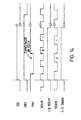
- the PLL By constructing the PLL as described above, signals are obtained at the timing shown in FIGURE 14. For instance, in the wide aspect conversion, the system must be operated based on the HREF signal which is in conformity with the horizontal synch, frequency. Therefore, a clear signal is generated using the 1824 fH which is the read clock in this embodiment.
- the PLL In the VCO system shown in the embodiment, the PLL is constructed based on this 1824 fH but it is expected that the 1824 fH read clock and the 1368 fH write clock generate about 10 ns jitter depending on such external conditions as fluctuation of analog devices, temperature change and the like. As a result, there were such malfunctions generated as subtle clock phases shift, generation of one clock shift. generation of one clock jitter, resulting in notching the vertical lines and the like.
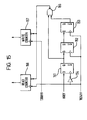
- FIGURE 15 shows means for solving the malfunctions involved in the embodiment shown in FIGURE 13 by simultaneously clearing the read counter 156 or generating the read timing and the write counter 157 for generating the write timing.
- FIGURE 15 will be explained by comparing it with FIGURE 14.
- the clear timing shown in FIGURE 14 is generated based on the HREF signal by the read clock 1824 fH using flip-flops 151 through 153, an inverter 154 and an NAND gate 155.
- the clear signal is generated by 1824 fH but this clearing signal also must clear circuits generated by 1368 fH.
- a clearing circuit used in counters uses a sync clearing system synchronizing with the leading edge of a clock in order to synchronize with the clock. At least more than one leading edge of 1368 fH must be contained in the clearing section of the clearing signal so that the clearing position does not move even when a clock jitter equivalent to 10 ns is generated.
- RCK a read clock
- the 1/16 times frequency division signal is input to a phase comparator 162 and is compared with the phase of a signal input through another input terminal.
- the phase error signal generated after the phase comparison is input to a VCO 163.
- the output clock of the VCO 163 becomes a write clock WCK.
- the output of the VCO 163 serves as a clock signal, and at the same time be input to a variable divider 164.
- This variable divider 164 controls a dividing ratio by an external control signal, i.e., a control signal supplied from the outside.
- the write clock WCK is variably divided by the variable divider 164 and input to another input terminal of the phase comparator 162.
- the output signal frequency of the variable divider 164 becomes 30/16 MHz.
- the write clock WCK becomes 30/2 MHz and the 1/2 times compression aspect conversion is achieved.
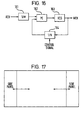
- FIGURE 17 is a schematic diagram showing a picture when an aspect ratio of the wide television screen is varied.
- variable divider 181 when a compression/expansion selecting signal is applied to a variable divider 181, it is possible to achieve. for instance, 1/2 times through 2 times variable division and expanders in simple construction as shown in FIGURE 18.
- the present invention can provide an extremely preferable time-base conversion system which is capable of compressing the time-base by varying write clock based on memory read clock, making a circuit scale small, keeping read clock frequency constant even when using a large compression ratio, thus achieving a large compression ratio easily and selecting optimum pre-filters in varied compression modes, it is possible to obtain extremely satisfactory high resolution video signals and satisfactory reproduced pictures without single clock Jitter even when the system uses different read and write clock frequencies.
Landscapes
- Engineering & Computer Science (AREA)
- Multimedia (AREA)
- Signal Processing (AREA)
- Computer Graphics (AREA)
- Television Signal Processing For Recording (AREA)
- Television Systems (AREA)
Claims (26)
- Un système de conversion de base de temps pour récepteur de télévision, comprenant :de premiers moyens de formation d'impulsions d'horloge pour produire une impulsion d'horloge de lecture sur la base d'un signal de référence ;de seconds moyens de formation d'impulsion d'horloge pour produire une impulsion d'horloge d'écriture par division de l'impulsion d'horloge de lecture ;une mémoire ;des moyens pour inscrire des données vidéo dans la mémoire sur la base de l'impulsion d'horloge d'écriture ;des moyens pour lire les données vidéo enregistrées dans la mémoire sur la base de l'impulsion d'horloge de lecture ; etdes moyens de compression de base de temps pour déterminer un rapport de compression de la base de temps des données vidéo par détermination d'un rapport de division de l'impulsion d'horloge d'écriture.
- Un système de conversion de base de temps pour récepteur de télévision comprenant :de premiers moyens de formation d'impulsions d'horloge pour produire une impulsion d'horloge de lecture sur la base d'un signal de référence ;de seconds moyens de formation d'impulsions d'horloge pour produire une impulsion d'horloge d'écriture par multiplication de l'impulsion d'horloge de lecture ;une mémoire ;des moyens pour inscrire des données vidéo dans la mémoire sur la base de l'impulsion d'horloge d'écriture ;des moyens pour lire les données vidéo enregistrées dans la mémoire sur la base de l'impulsion d'horloge de lecture ; etdes moyens de dilatation de base de temps pour déterminer un rapport de dilatation de la base de temps des données vidéo par détermination d'un rapport de multiplication de l'impulsion d'horloge d'écriture.
- Un système de conversion de base de temps tel que revendiqué à la revendication 1 ou 2, dans lequel la mémoire est une mémoire à semi-conducteur.
- Un système de conversion de base de temps tel que revendiqué à la revendication 3, dans lequel la mémoire à semi-conducteur est une mémoire du type à deux accès.
- Un système de conversion de base de temps tel que revendiqué à la revendication 1, dans lequel les moyens de compression de base de temps comprennent des moyens pour convertir un format d'image d'une image de télévision en un autre format d'image.
- Un système de conversion de base de temps tel que revendiqué à la revendication 2, dans lequel les moyens de dilatation de base de temps comprennent des moyens pour convertir un format d'image d'une image de télévision en un autre format d'image.
- Un système de conversion de base de temps tel que revendiqué à la revendication 1 ou 2, dans lequel l'impulsion d'horloge de lecture et l'impulsion d'horloge d'écriture sont des multiples entiers d'une période de balayage horizontale des signaux de télévision.
- Un système de conversion de base de temps tel que revendiqué à la revendication 1, dans lequel l'impulsion d'horloge de lecture est produite par une division par l'intermédiaire d'un diviseur de fréquence programmable.
- Un système de conversion de base de temps tel que revendiqué à la revendication 1, dans lequel l'impulsion d'horloge de lecture est produite par une division par l'intermédiaire d'une boucle à phase asservie.
- Un système de conversion de base de temps tel que revendiqué à la revendication 8 ou 9, dans lequel les moyens de formation d'impulsion d'horloges sont constitués par un type de diviseur de fréquence programmable dans lequel l'impulsion d'horloge d'écriture est produite à partir d'un oscillateur commandé en tension, et dans lequel la fréquence de l'impulsion d'horloge produite par l'oscillateur commandé en tension est commandée par un signal de comparaison de phase d'un signal obtenu en divisant la sortie de l'oscillateur commandé en tension par un facteur de N (N est un nombre entier supérieur à 1) par l'intermédiaire d'un premier diviseur de fréquence et d'un signal obtenu en divisant une seconde impulsion d'horloge de lecture par un facteur de M (M est un nombre entier supérieur à 1) par l'intermédiaire d'un second diviseur de fréquence, puis le premier rapport de division est modifié en commandant le premier diviseur de fréquence par un signal de commande externe.
- Un système de conversion de base de temps tel que revendiqué à la revendication 10, dans lequel le premier diviseur de fréquence est composé d'un circuit numérique, et dans lequel le signal de commande externe devant être appliqué au premier diviseur de fréquence est un signal numérique.
- Un système de conversion de base de temps tel que revendiqué à la revendication 10, dans lequel le premier diviseur de fréquence est composé d'un circuit analogique, et dans lequel le signal de commande externe devant être appliqué au premier diviseur de fréquence est un signal analogique.
- Un système de conversion de base de temps tel que revendiqué à la revendication 9, dans lequel la boucle à phase asservie est composée d'un oscillateur commandé en tension pour produire l'impulsion d'horloge d'écriture, d'un comparateur de phase présentant une première borne d'entrée prévue pour recevoir l'impulsion d'horloge d'écriture, par l'intermédiaire d'une division de fréquence, une seconde borne d'entrée prévue pour recevoir l'impulsion d'horloge de lecture et une borne de sortie pour appliquer le résultat de sa comparaison de phase en retour à l'oscillateur commandé en tension sous la forme d'un signal de commande.
- Un système de conversion de base de temps tel que revendiqué à la revendication 9, dans lequel la boucle à phase asservie est composée d'un oscillateur commandé en tension pour produire l'impulsion d'horloge d'écriture, d'un comparateur de phase présentant une première borne d'entrée prévue pour recevoir l'impulsion d'horloge d'écriture, une seconde borne d'entrée prévue pour recevoir l'impulsion d'horloge de lecture par l'intermédiaire d'une division de fréquence et une borne de sortie pour appliquer le résultat de sa comparaison de phase en retour à l'oscillateur commandé en tension sous la forme d'un signal de commande.
- Un système de conversion de base de temps tel que revendiqué à la revendication 2, dans lequel l'impulsion d'horloge de lecture est produite par une multiplication par l'intermédiaire d'un diviseur de fréquence programmable.
- Un système de conversion de base de temps tel que revendiqué à la revendication 2, dans lequel l'impulsion d'horloge de lecture est produite par une multiplication par l'intermédiaire d'une boucle à phase asservie.
- Un système de conversion de base de temps tel que revendiqué à la revendication 15 ou 16, dans lequel les moyens de formation d'impulsions d'horloge sont constitués par un type de multiplicateur de fréquence programmable dans lequel l'impulsion d'horloge d'écriture est produite à partir d'un oscillateur commandé en tension, et dans lequel la fréquence de l'impulsion d'horloge produite par l'oscillateur commandé en tension est commandée par un signal de comparaison de phase d'un signal obtenu en divisant la sortie de l'oscillateur commandé en tension par un facteur de N (N est un nombre entier supérieur à 1) par l'intermédiaire d'un premier diviseur de fréquence et d'un signal obtenu en divisant une seconde impulsion d'horloge de lecture par un facteur de M (M est un nombre entier supérieur à 1) par l'intermédiaire d'un second diviseur de fréquence, puis le premier rapport de division est modifié en commandant le premier diviseur de fréquence par un signal de commande externe.
- Un système de conversion de base de temps tel que revendiqué à la revendication 17, dans lequel le premier diviseur de fréquence est composé d'un circuit numérique, et dans lequel le signal de commande externe devant être appliqué au premier diviseur de fréquence est un signal numérique.
- Un système de conversion de base de temps tel que revendiqué à la revendication 17, dans lequel le premier diviseur de fréquence est composé d'un circuit analogique, et dans lequel le signal de commande externe devant être appliqué au premier diviseur de fréquence est un signal analogique.
- Un système de conversion de base de temps tel que revendiqué à la revendication 16, dans lequel la boucle à phase asservie est composée d'un oscillateur commandé en tension pour produire l'impulsion d'horloge d'écriture, d'un comparateur de phase présentant une première borne d'entrée prévue pour recevoir l'impulsion d'horloge d'écriture par l'intermédiaire d'une division de fréquence, une seconde borne d'entrée prévue pour recevoir l'impulsion d'horloge de lecture et une borne de sortie pour appliquer le résultat de sa comparaison de phase en retour à l'oscillateur commandé en tension sous la forme d'un signal de commande.
- Un système de conversion de base de tension tel que revendiqué à la revendication 16, dans lequel la boucle à phase asservie est composée d'un oscillateur commandé en tension pour produire l'impulsion d'horloge d'écriture, d'un comparateur de phase présentant une première borne d'entrée prévue pour recevoir l'impulsion d'horloge d'écriture, une seconde borne d'entrée prévue pour recevoir l'impulsion d'horloge de lecture par l'intermédiaire d'une division de fréquence et une borne de sortie pour appliquer le résultat de sa comparaison de phase en retour à l'oscillateur commandé en tension sous la forme d'un signal de commande.
- Un système de conversion de base de temps tel que revendiqué à la revendication 1, dans lequel la fréquence de l'impulsion d'horloge de lecture est égale à 1824 fois la fréquence de synchronisation horizontale du signal vidéo d'entrée.
- Un système de conversion de base de temps tel que revendiqué à la revendication 1, dans lequel la fréquence de l'impulsion d'horloge de lecture est égale à 1808 fois la fréquence de synchronisation horizontale du signal vidéo d'entrée.
- Un système de conversion de base de temps tel que revendiqué dans une quelconque revendication précédente, comprenant des moyens pour convertir un signal vidéo analogique d'entrée et former le signal de données vidéo numérique,dans lequel le signal de référence des premiers moyens de formation d'impulsions d'horloge est basé sur un signal de synchronisation horizontal, etdans lequel la conversion de la base de temps est utilisée pour convertir un format d'image du signal vidéo,le système comprenant en outre des filtres présentant différentes caractéristiques de fréquence pour éliminer une erreur d'effet d'escalier dans la conversion du signal vidéo analogique pour former le signal vidéo numérique, et des moyens pour sélectionner un filtre présentant une caractéristique de fréquence optimale correspondant à un format d'image désiré sélectionné par un signal pour sélectionner le format d'image.
- Un système de conversion de base de temps tel que revendiqué à la revendication 24, dans lequel chacun des filtres éliminant l'erreur d'effet d'escalier et des moyens de sélection de filtre est un dispositif de commutation de filtre comprenant un circuit analogique.
- Un système de conversion de base de temps tel que revendiqué à la revendication 24, dans lequel chacun des filtres éliminant l'erreur d'effet d'escalier et des moyens de sélection de filtre est un dispositif de commutation de filtre comprenant un circuit numérique.
Applications Claiming Priority (3)
| Application Number | Priority Date | Filing Date | Title |
|---|---|---|---|
| JP08982594A JP3556267B2 (ja) | 1994-04-27 | 1994-04-27 | 時間軸変換方式 |
| JP8982594 | 1994-04-27 | ||
| JP89825/94 | 1994-04-27 |
Publications (2)
| Publication Number | Publication Date |
|---|---|
| EP0680210A1 EP0680210A1 (fr) | 1995-11-02 |
| EP0680210B1 true EP0680210B1 (fr) | 2001-08-29 |
Family
ID=13981538
Family Applications (1)
| Application Number | Title | Priority Date | Filing Date |
|---|---|---|---|
| EP95302840A Expired - Lifetime EP0680210B1 (fr) | 1994-04-27 | 1995-04-27 | Système de conversion de base de temps |
Country Status (6)
| Country | Link |
|---|---|
| US (1) | US5648820A (fr) |
| EP (1) | EP0680210B1 (fr) |
| JP (1) | JP3556267B2 (fr) |
| KR (1) | KR100204432B1 (fr) |
| CA (1) | CA2148033C (fr) |
| DE (1) | DE69522362T2 (fr) |
Families Citing this family (8)
| Publication number | Priority date | Publication date | Assignee | Title |
|---|---|---|---|---|
| GB9501784D0 (en) * | 1995-01-30 | 1995-03-22 | Rca Thomson Licensing Corp | Displaying 4:3 image on 16:9 tube |
| US5926224A (en) * | 1995-07-31 | 1999-07-20 | Sony Corporation | Imaging, system, video processing apparatus, encoding apparatus, encoding method, and method of removing random noise |
| KR100195129B1 (ko) * | 1996-02-21 | 1999-06-15 | 윤종용 | 가정용 hdtv 카메라를 위한 수직라인 배속 변환방법 및 그 회로 |
| JP2000092409A (ja) * | 1998-09-10 | 2000-03-31 | Sony Corp | 映像表示装置 |
| KR100429874B1 (ko) * | 2001-07-20 | 2004-05-04 | 삼성전자주식회사 | 파노라마/워터글라스 기능 구현을 위한 영상 처리 장치 및그 방법 |
| KR100604009B1 (ko) * | 2003-12-15 | 2006-07-24 | 엘지전자 주식회사 | 창문형 공조장치 및 그 구동 방법 |
| JP4778872B2 (ja) * | 2005-10-20 | 2011-09-21 | パナソニック株式会社 | 楽音出力装置 |
| CN116318155B (zh) * | 2023-05-19 | 2023-08-11 | 武汉普赛斯电子股份有限公司 | 一种精密时基等效采样装置及方法 |
Family Cites Families (14)
| Publication number | Priority date | Publication date | Assignee | Title |
|---|---|---|---|---|
| JPS59172897A (ja) * | 1983-03-22 | 1984-09-29 | Victor Co Of Japan Ltd | カラ−映像信号再生装置におけるクロツクパルス発生回路 |
| US4691248A (en) * | 1983-07-14 | 1987-09-01 | Victor Company Of Japan | Synchronized signal separating circuit for a recording and reproducing apparatus |
| US4651208A (en) * | 1985-03-18 | 1987-03-17 | Scientific Atlanta, Inc. | Compatibility of widescreen and non-widescreen television transmissions |
| FR2606576B1 (fr) * | 1986-11-07 | 1989-02-03 | Labo Electronique Physique | Dispositif pour transmettre des images de television haute definition dans des canaux a bande etroite |
| JP2619455B2 (ja) * | 1988-01-29 | 1997-06-11 | 株式会社日立製作所 | 映像信号の記録方法ならびに再生方法およびこれらを用いた装置 |
| JPH0220183A (ja) * | 1988-07-08 | 1990-01-23 | Mitsubishi Electric Corp | 走査線変換装置 |
| NL8902113A (nl) * | 1989-08-22 | 1991-03-18 | Philips Nv | Beeldweergeefinrichting en videosignaalverwerkingsschakeling. |
| JPH04124983A (ja) * | 1990-09-17 | 1992-04-24 | Pioneer Electron Corp | 画像表示システム |
| JP2673386B2 (ja) * | 1990-09-29 | 1997-11-05 | シャープ株式会社 | 映像表示装置 |
| KR0159109B1 (ko) * | 1991-09-19 | 1999-01-15 | 강진구 | 화상신호의 종횡비 및 주사선 수 변환장치 |
| JP2904975B2 (ja) * | 1991-10-30 | 1999-06-14 | 三菱電機株式会社 | ワイドアスペクト比のテレビジョン受信機 |
| EP0545341B1 (fr) * | 1991-11-29 | 1997-09-17 | Sanyo Electric Co., Ltd. | Récepteur de télévision |
| JPH05207326A (ja) * | 1992-01-28 | 1993-08-13 | Matsushita Electric Ind Co Ltd | 水平圧縮pll回路 |
| US5349385A (en) * | 1992-08-06 | 1994-09-20 | Florida Atlantic University | Adaptive scan converter |
-
1994
- 1994-04-27 JP JP08982594A patent/JP3556267B2/ja not_active Expired - Fee Related
-
1995
- 1995-04-26 US US08/427,959 patent/US5648820A/en not_active Expired - Fee Related
- 1995-04-27 KR KR1019950010049A patent/KR100204432B1/ko not_active Expired - Fee Related
- 1995-04-27 CA CA002148033A patent/CA2148033C/fr not_active Expired - Fee Related
- 1995-04-27 DE DE69522362T patent/DE69522362T2/de not_active Expired - Fee Related
- 1995-04-27 EP EP95302840A patent/EP0680210B1/fr not_active Expired - Lifetime
Also Published As
| Publication number | Publication date |
|---|---|
| JPH07298206A (ja) | 1995-11-10 |
| DE69522362D1 (de) | 2001-10-04 |
| CA2148033C (fr) | 2004-08-17 |
| US5648820A (en) | 1997-07-15 |
| KR100204432B1 (ko) | 1999-06-15 |
| KR950030716A (ko) | 1995-11-24 |
| DE69522362T2 (de) | 2002-02-07 |
| EP0680210A1 (fr) | 1995-11-02 |
| JP3556267B2 (ja) | 2004-08-18 |
| CA2148033A1 (fr) | 1995-10-28 |
Similar Documents
| Publication | Publication Date | Title |
|---|---|---|
| US4712130A (en) | Chrominance signal frequency converter as for a pix-in-pix television receiver | |
| KR100195358B1 (ko) | 라인 메모리 및 제어 시스템 | |
| JP2715172B2 (ja) | 信号濾波装置 | |
| US5442406A (en) | Wide screen television | |
| US5134479A (en) | NTSC high resolution television converting apparatus for converting television signals of an NTSC system into high resolution television signals | |
| EP0229431A2 (fr) | Récepteur de télévision couleur à insertion d'image | |
| JPH09507015A (ja) | 時間基準補正を用いるテレビジョンデジタル信号処理装置 | |
| JPH05252457A (ja) | 拡大画面表示回路 | |
| US6556249B1 (en) | Jitter cancellation technique for video clock recovery circuitry | |
| EP0680210B1 (fr) | Système de conversion de base de temps | |
| US5638131A (en) | Method to synchronize video modulation using a constant time base | |
| JPS6184183A (ja) | 順次走査ビデオ・プロセツサ | |
| US5303061A (en) | Apparatus for rejecting time base error of video signal | |
| US6453109B1 (en) | Video-signal processing apparatus providing a first clock signal and second clock signal which is based on the phase of the input signal | |
| US5629962A (en) | Phase locked loop circuit | |
| JP3405208B2 (ja) | 分割マルチ画面表示装置 | |
| EP0582305B1 (fr) | Dispositif de conversion de signal vidéo et éliminateur de bruit | |
| US5534939A (en) | Digital video clock generation system | |
| JP2944284B2 (ja) | 多画面表示装置 | |
| JPS62271584A (ja) | 映像信号処理方法 | |
| JPH118799A (ja) | ビデオ表示制御装置 | |
| JP3129866B2 (ja) | アスペクト比変換装置 | |
| JPH077744A (ja) | タイムベースコレクタ装置 | |
| JPH07134575A (ja) | 映像信号変換装置 | |
| JPH06253337A (ja) | タイムベースコレクタ装置 |
Legal Events
| Date | Code | Title | Description |
|---|---|---|---|
| PUAI | Public reference made under article 153(3) epc to a published international application that has entered the european phase |
Free format text: ORIGINAL CODE: 0009012 |
|
| 17P | Request for examination filed |
Effective date: 19950502 |
|
| AK | Designated contracting states |
Kind code of ref document: A1 Designated state(s): DE FR GB NL |
|
| 17Q | First examination report despatched |
Effective date: 19971007 |
|
| GRAG | Despatch of communication of intention to grant |
Free format text: ORIGINAL CODE: EPIDOS AGRA |
|
| GRAG | Despatch of communication of intention to grant |
Free format text: ORIGINAL CODE: EPIDOS AGRA |
|
| GRAH | Despatch of communication of intention to grant a patent |
Free format text: ORIGINAL CODE: EPIDOS IGRA |
|
| GRAH | Despatch of communication of intention to grant a patent |
Free format text: ORIGINAL CODE: EPIDOS IGRA |
|
| GRAA | (expected) grant |
Free format text: ORIGINAL CODE: 0009210 |
|
| AK | Designated contracting states |
Kind code of ref document: B1 Designated state(s): DE FR GB NL |
|
| PG25 | Lapsed in a contracting state [announced via postgrant information from national office to epo] |
Ref country code: NL Free format text: LAPSE BECAUSE OF FAILURE TO SUBMIT A TRANSLATION OF THE DESCRIPTION OR TO PAY THE FEE WITHIN THE PRESCRIBED TIME-LIMIT Effective date: 20010829 |
|
| REF | Corresponds to: |
Ref document number: 69522362 Country of ref document: DE Date of ref document: 20011004 |
|
| REG | Reference to a national code |
Ref country code: GB Ref legal event code: IF02 |
|
| EN | Fr: translation not filed | ||
| NLV1 | Nl: lapsed or annulled due to failure to fulfill the requirements of art. 29p and 29m of the patents act | ||
| PLBE | No opposition filed within time limit |
Free format text: ORIGINAL CODE: 0009261 |
|
| STAA | Information on the status of an ep patent application or granted ep patent |
Free format text: STATUS: NO OPPOSITION FILED WITHIN TIME LIMIT |
|
| 26N | No opposition filed | ||
| ET | Fr: translation filed | ||
| REG | Reference to a national code |
Ref country code: FR Ref legal event code: ERR Free format text: BOPI DE PUBLICATION N: 02/04 PAGES: 241 PARTIE DU BULLETIN CONCERNEE: BREVETS EUROPEENS DONT LA TRADUCTION N'A PAS ETE REMISE A I'INPI IL Y A LIEU DE SUPPRIMER: LA MENTION DE LA NON REMISE. LA REMISE DE CETTE TRADUCTION EST PUBLIEE DANS LE PRESENT BOPI. |
|
| PGFP | Annual fee paid to national office [announced via postgrant information from national office to epo] |
Ref country code: FR Payment date: 20080312 Year of fee payment: 14 Ref country code: DE Payment date: 20080502 Year of fee payment: 14 |
|
| PGFP | Annual fee paid to national office [announced via postgrant information from national office to epo] |
Ref country code: GB Payment date: 20080430 Year of fee payment: 14 |
|
| GBPC | Gb: european patent ceased through non-payment of renewal fee |
Effective date: 20090427 |
|
| REG | Reference to a national code |
Ref country code: FR Ref legal event code: ST Effective date: 20091231 |
|
| PG25 | Lapsed in a contracting state [announced via postgrant information from national office to epo] |
Ref country code: DE Free format text: LAPSE BECAUSE OF NON-PAYMENT OF DUE FEES Effective date: 20091103 |
|
| PG25 | Lapsed in a contracting state [announced via postgrant information from national office to epo] |
Ref country code: GB Free format text: LAPSE BECAUSE OF NON-PAYMENT OF DUE FEES Effective date: 20090427 Ref country code: FR Free format text: LAPSE BECAUSE OF NON-PAYMENT OF DUE FEES Effective date: 20091222 |