EP0681331A2 - Verbesserungen in oder an dynamische Speicheranordnungen mit wahlfreiem Zugriff - Google Patents
Verbesserungen in oder an dynamische Speicheranordnungen mit wahlfreiem Zugriff Download PDFInfo
- Publication number
- EP0681331A2 EP0681331A2 EP95302940A EP95302940A EP0681331A2 EP 0681331 A2 EP0681331 A2 EP 0681331A2 EP 95302940 A EP95302940 A EP 95302940A EP 95302940 A EP95302940 A EP 95302940A EP 0681331 A2 EP0681331 A2 EP 0681331A2
- Authority
- EP
- European Patent Office
- Prior art keywords
- substrate
- section
- bias voltage
- substrate layer
- forming
- Prior art date
- Legal status (The legal status is an assumption and is not a legal conclusion. Google has not performed a legal analysis and makes no representation as to the accuracy of the status listed.)
- Granted
Links
Images
Classifications
-
- H—ELECTRICITY
- H10—SEMICONDUCTOR DEVICES; ELECTRIC SOLID-STATE DEVICES NOT OTHERWISE PROVIDED FOR
- H10B—ELECTRONIC MEMORY DEVICES
- H10B12/00—Dynamic random access memory [DRAM] devices
- H10B12/30—DRAM devices comprising one-transistor - one-capacitor [1T-1C] memory cells
-
- H—ELECTRICITY
- H10—SEMICONDUCTOR DEVICES; ELECTRIC SOLID-STATE DEVICES NOT OTHERWISE PROVIDED FOR
- H10B—ELECTRONIC MEMORY DEVICES
- H10B12/00—Dynamic random access memory [DRAM] devices
- H10B12/01—Manufacture or treatment
- H10B12/09—Manufacture or treatment with simultaneous manufacture of the peripheral circuit region and memory cells
-
- H—ELECTRICITY
- H10—SEMICONDUCTOR DEVICES; ELECTRIC SOLID-STATE DEVICES NOT OTHERWISE PROVIDED FOR
- H10D—INORGANIC ELECTRIC SEMICONDUCTOR DEVICES
- H10D84/00—Integrated devices formed in or on semiconductor substrates that comprise only semiconducting layers, e.g. on Si wafers or on GaAs-on-Si wafers
- H10D84/01—Manufacture or treatment
- H10D84/0123—Integrating together multiple components covered by H10D12/00 or H10D30/00, e.g. integrating multiple IGBTs
- H10D84/0126—Integrating together multiple components covered by H10D12/00 or H10D30/00, e.g. integrating multiple IGBTs the components including insulated gates, e.g. IGFETs
- H10D84/0156—Manufacturing their doped wells
Definitions
- the present invention relates in general to semiconductor fabrication processes and devices and more particularly to an apparatus and method of fabricating a multiple substrate bias dynamic random access memory device.
- DRAM Dynamic random access memory
- DRAM Dynamic random access memory
- the substrate bias enhances an undesirable short channel effect.
- This short channel effect produces a large threshold voltage difference between devices of different sizes when the substrate bias voltage is applied.
- Such a large difference between devices of different sizes make the control of the threshold voltage very difficult.
- Attempts to overcome this short channel effect problem include using triple well isolation to allow for different substrate biases to be applied to different parts of the dynamic random access memory.
- the triple well approach uses an unconventional n- type substrate and isolation with various p-type wells.
- the depth of the p- type wells limit the depth for a trench in the memory array of the DRAM device. Since the trench wall is doped with an N+ conductivity type, any contact of the trench with the n- type substrate will short the trenches together. Therefore, it is desirable to overcome the short channel effect and trench depth problems through a more conventional process.
- an apparatus and method of fabricating a multiple substrate bias dynamic random access memory device are provided which substantially eliminate or reduce disadvantages and problems associated with other processes attempting to overcome the short channel effect.
- a method of fabricating a multiple substrate bias dynamic random access memory device that includes forming an input/output section within a substrate layer where the input/output section operates from a first substrate bias voltage.
- a peripheral transistor section is formed within the substrate layer such that the peripheral transistor section can operate from a second substrate bias voltage.
- a memory array section is formed within the substrate layer such that the memory array section can operate from a third substrate bias voltage.
- the apparatus and method of the present invention provides various technical advantages over other processes attempting to overcome the short channel effect.
- one technical advantage is in employing a conventional p- type substrate layer to overcome the short channel effect.
- Another technical advantage is in overcoming the short channel effect through multiple substrate bias voltage implementation.
- Other technical advantages are readily apparent to one skilled in the art from the following figures, descriptions, and claims.
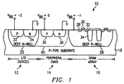
- FIGURE 1 illustrates a multiple substrate bias dynamic random access memory device.
- FIGURE 1 shows a dynamic random access memory device 10 which can employ multiple substrate bias voltages.
- Dynamic random access memory device 10 is made up of at least three distinct sections - an input/output section 12, a peripheral transistor section 14, and a memory array section 16. Each section of dynamic random access memory device 10 can be individually isolated on a p-type substrate layer 18.
- Input/output section 12 is made by forming an n- type well region 20 within p- type substrate layer 18.
- a p- type region 22 and an n- type region 24 are formed within n- type well region 20.
- n- type well region 20 isolates p- type region 22 from p- type substrate layer 18.
- Memory array section 16 is made by forming a p- type well region 26 within p- type substrate layer 18. Multiple subdevices having a source region 28, a gate region 30, and a drain region 32 are formed within p- type well region 26. The multiple subdevices of memory array section 16 are isolated by trenches 34.
- Peripheral transistor section 14 is made by forming a p- type region 36 and an n- type region 38 within p- type substrate layer 18. If isolation is required between peripheral transistor section 14 and memory array section 16, an optional n- type well region 40 can be formed prior to forming p- type region 36 and n- type region 38 in order to isolate p- type region 36 from p- type substrate layer 18.
- n- type well region 40 dynamic random access memory device 10 can operate with three separate substrate bias voltages.
- a neutral substrate bias voltage of ground is applied to avoid any back gate biasing of transistors and suppress the short channel effects that result in a larger body effect on the threshold voltage.
- a different bias voltage may be applied to memory array section 16 in order to improve cell isolation and reduce junction capacitance. Since inter p- type well isolation is achieved by the n- type well region, which can be driven at the same time as the p- type well region 26 of memory array section 16, the need for an n-type substrate for well to well isolation is eliminated. Further, the trench step of trench 34 may be equal to or slightly deeper than p- type well region 26 without significantly increasing cell leakage in order that more capacitor area can be used.
- a dynamic random access memory device can overcome the short channel effect by employing multiple substrate bias voltages through a conventional p- type substrate layer.
- Each section of the dynamic random access memory device can be individually isolated and trench depth within the memory array section is no longer a critical factor.
Landscapes
- Engineering & Computer Science (AREA)
- Manufacturing & Machinery (AREA)
- Semiconductor Memories (AREA)
- Metal-Oxide And Bipolar Metal-Oxide Semiconductor Integrated Circuits (AREA)
- Bipolar Integrated Circuits (AREA)
- Dram (AREA)
Applications Claiming Priority (2)
| Application Number | Priority Date | Filing Date | Title |
|---|---|---|---|
| US08/236,745 US5595925A (en) | 1994-04-29 | 1994-04-29 | Method for fabricating a multiple well structure for providing multiple substrate bias for DRAM device formed therein |
| US236745 | 1994-04-29 |
Publications (3)
| Publication Number | Publication Date |
|---|---|
| EP0681331A2 true EP0681331A2 (de) | 1995-11-08 |
| EP0681331A3 EP0681331A3 (de) | 1997-09-03 |
| EP0681331B1 EP0681331B1 (de) | 2002-11-06 |
Family
ID=22890772
Family Applications (1)
| Application Number | Title | Priority Date | Filing Date |
|---|---|---|---|
| EP95302940A Expired - Lifetime EP0681331B1 (de) | 1994-04-29 | 1995-04-28 | Verbesserungen in oder an dynamische Speicheranordnungen mit wahlfreiem Zugriff |
Country Status (6)
| Country | Link |
|---|---|
| US (2) | US5595925A (de) |
| EP (1) | EP0681331B1 (de) |
| JP (1) | JPH088412A (de) |
| KR (1) | KR950034791A (de) |
| DE (1) | DE69528724T2 (de) |
| TW (1) | TW301054B (de) |
Cited By (2)
| Publication number | Priority date | Publication date | Assignee | Title |
|---|---|---|---|---|
| FR2769746A1 (fr) * | 1997-10-14 | 1999-04-16 | St Microelectronics Sa | Dispositif de memoire vive dynamique a duree de rafraichissement reduite, et procede correspondant de rafraichissement |
| FR2769745A1 (fr) * | 1997-10-14 | 1999-04-16 | St Microelectronics Sa | Dispositif de memoire vive dynamique |
Families Citing this family (19)
| Publication number | Priority date | Publication date | Assignee | Title |
|---|---|---|---|---|
| JP4037470B2 (ja) | 1994-06-28 | 2008-01-23 | エルピーダメモリ株式会社 | 半導体装置 |
| US5637902A (en) * | 1996-01-16 | 1997-06-10 | Vlsi Technology, Inc. | N-well resistor as a ballast resistor for output MOSFET |
| KR100189739B1 (ko) * | 1996-05-02 | 1999-06-01 | 구본준 | 반도체 기판에 삼중웰을 형성하는 방법 |
| US6750527B1 (en) * | 1996-05-30 | 2004-06-15 | Kabushiki Kaisha Toshiba | Semiconductor integrated circuit device having a plurality of wells, test method of testing the semiconductor integrated circuit device, and test device which executes the test method |
| US6674112B1 (en) * | 1997-06-27 | 2004-01-06 | Hitachi, Ltd. | Semiconductor integrated circuit device |
| US6133597A (en) * | 1997-07-25 | 2000-10-17 | Mosel Vitelic Corporation | Biasing an integrated circuit well with a transistor electrode |
| KR100275725B1 (ko) * | 1997-12-27 | 2000-12-15 | 윤종용 | 트리플웰 구조를 갖는 반도체 메모리 장치 및 그 제조방법 |
| KR100310470B1 (ko) * | 1997-12-30 | 2002-05-09 | 박종섭 | 양면반도체메모리소자및그제조방법 |
| JP2000183306A (ja) * | 1998-12-14 | 2000-06-30 | Fujitsu Ltd | 半導体記憶装置 |
| US6258641B1 (en) | 1999-02-05 | 2001-07-10 | Taiwan Semiconductor Manufacturing Company | OTP (open trigger path) latchup scheme using triple and buried well for sub-quarter micron transistors |
| US8389370B2 (en) * | 1999-08-02 | 2013-03-05 | Schilmass Co. L.L.C. | Radiation-tolerant integrated circuit device and method for fabricating |
| KR100304710B1 (ko) * | 1999-08-30 | 2001-11-01 | 윤종용 | 셀 어레이 영역내에 벌크 바이어스 콘택 구조를 구비하는 비휘발성 메모리소자 |
| JP2001291779A (ja) * | 2000-04-05 | 2001-10-19 | Mitsubishi Electric Corp | 半導体装置およびその製造方法 |
| KR100393201B1 (ko) * | 2001-04-16 | 2003-07-31 | 페어차일드코리아반도체 주식회사 | 낮은 온 저항과 높은 브레이크다운 전압을 갖는 고전압수평형 디모스 트랜지스터 |
| KR100468787B1 (ko) * | 2003-05-02 | 2005-01-29 | 삼성전자주식회사 | 래치-업(Latch-up)에 의한 전류 흐름을 방지할 수있는 반도체 장치 |
| US6885054B1 (en) * | 2004-02-04 | 2005-04-26 | Texas Instruments Incorporated | Threshold voltage stabilizer, method of manufacturing and integrated circuit employing the same |
| KR100685620B1 (ko) * | 2006-02-16 | 2007-02-22 | 주식회사 하이닉스반도체 | 반도체 소자 및 그 제조 방법 |
| JP5174434B2 (ja) * | 2007-11-16 | 2013-04-03 | ルネサスエレクトロニクス株式会社 | 半導体装置 |
| KR20140042459A (ko) | 2012-09-28 | 2014-04-07 | 삼성전자주식회사 | 멀티플 웰 바이어스 메모리 장치 |
Family Cites Families (15)
| Publication number | Priority date | Publication date | Assignee | Title |
|---|---|---|---|---|
| US3916430A (en) * | 1973-03-14 | 1975-10-28 | Rca Corp | System for eliminating substrate bias effect in field effect transistor circuits |
| JPH0671067B2 (ja) * | 1985-11-20 | 1994-09-07 | 株式会社日立製作所 | 半導体装置 |
| US5324982A (en) * | 1985-09-25 | 1994-06-28 | Hitachi, Ltd. | Semiconductor memory device having bipolar transistor and structure to avoid soft error |
| GB2199695B (en) * | 1987-01-06 | 1990-07-25 | Samsung Semiconductor Inc | Dynamic random access memory with selective well biasing |
| EP0298421B1 (de) * | 1987-07-10 | 1993-12-15 | Kabushiki Kaisha Toshiba | Halbleiterbauelement mit Bereichen unterschiedlicher Störstellenkonzentration |
| US5260226A (en) * | 1987-07-10 | 1993-11-09 | Kabushiki Kaisha Toshiba | Semiconductor device having different impurity concentration wells |
| JPH03276673A (ja) * | 1990-03-26 | 1991-12-06 | Matsushita Electric Ind Co Ltd | 半導体記憶装置 |
| KR950009893B1 (ko) * | 1990-06-28 | 1995-09-01 | 미쓰비시 뎅끼 가부시끼가이샤 | 반도체기억장치 |
| JP3128262B2 (ja) * | 1991-05-28 | 2001-01-29 | 株式会社東芝 | 半導体集積回路装置 |
| JP3125943B2 (ja) * | 1991-09-17 | 2001-01-22 | 日本電信電話株式会社 | 半導体装置の製造方法 |
| KR950009815B1 (ko) * | 1991-12-23 | 1995-08-28 | 삼성전자주식회사 | 트리플웰 구조를 가지는 고집적 반도체 메모리 장치 |
| DE69229717T2 (de) * | 1992-01-09 | 2000-03-02 | International Business Machines Corp., Armonk | Matrix von Graben-DRAM-Zellen |
| US5264716A (en) * | 1992-01-09 | 1993-11-23 | International Business Machines Corporation | Diffused buried plate trench dram cell array |
| KR940003026A (ko) * | 1992-07-13 | 1994-02-19 | 김광호 | 트리플웰을 이용한 반도체장치 |
| US5422294A (en) * | 1993-05-03 | 1995-06-06 | Noble, Jr.; Wendell P. | Method of making a trench capacitor field shield with sidewall contact |
-
1994
- 1994-04-29 US US08/236,745 patent/US5595925A/en not_active Expired - Lifetime
-
1995
- 1995-04-28 EP EP95302940A patent/EP0681331B1/de not_active Expired - Lifetime
- 1995-04-28 DE DE69528724T patent/DE69528724T2/de not_active Expired - Lifetime
- 1995-04-29 KR KR1019950010626A patent/KR950034791A/ko not_active Ceased
- 1995-05-01 JP JP7142314A patent/JPH088412A/ja active Pending
- 1995-11-17 TW TW084112187A patent/TW301054B/zh not_active IP Right Cessation
-
1997
- 1997-08-12 US US08/909,904 patent/US5894145A/en not_active Expired - Lifetime
Cited By (6)
| Publication number | Priority date | Publication date | Assignee | Title |
|---|---|---|---|---|
| FR2769746A1 (fr) * | 1997-10-14 | 1999-04-16 | St Microelectronics Sa | Dispositif de memoire vive dynamique a duree de rafraichissement reduite, et procede correspondant de rafraichissement |
| FR2769745A1 (fr) * | 1997-10-14 | 1999-04-16 | St Microelectronics Sa | Dispositif de memoire vive dynamique |
| EP0910093A1 (de) * | 1997-10-14 | 1999-04-21 | STMicroelectronics SA | Dynamische Speicheranordnung |
| EP0910094A1 (de) * | 1997-10-14 | 1999-04-21 | STMicroelectronics SA | Dynamische Speicheranordnung mit verkürzter Auffrischungszeit und entsprechende Auffrischungsverfahren |
| US6002628A (en) * | 1997-10-14 | 1999-12-14 | Stmicroelectronics S.A. | Dynamic random access memory device with reduced refresh duration, and corresponding refresh process |
| US6177694B1 (en) | 1997-10-14 | 2001-01-23 | Stmicroelectronics S.A. | Dynamic random access memory device |
Also Published As
| Publication number | Publication date |
|---|---|
| US5595925A (en) | 1997-01-21 |
| EP0681331A3 (de) | 1997-09-03 |
| KR950034791A (ko) | 1995-12-28 |
| US5894145A (en) | 1999-04-13 |
| DE69528724T2 (de) | 2003-09-18 |
| JPH088412A (ja) | 1996-01-12 |
| DE69528724D1 (de) | 2002-12-12 |
| TW301054B (de) | 1997-03-21 |
| EP0681331B1 (de) | 2002-11-06 |
Similar Documents
| Publication | Publication Date | Title |
|---|---|---|
| US5595925A (en) | Method for fabricating a multiple well structure for providing multiple substrate bias for DRAM device formed therein | |
| KR100275725B1 (ko) | 트리플웰 구조를 갖는 반도체 메모리 장치 및 그 제조방법 | |
| US6211003B1 (en) | Semiconductor integrated circuit device and process for manufacturing the same | |
| US5170232A (en) | MOS field-effect transistor with sidewall spacers | |
| US7375398B2 (en) | High voltage FET gate structure | |
| JP2001352077A (ja) | Soi電界効果トランジスタ | |
| US5970338A (en) | Method of producing an EEPROM semiconductor structure | |
| US4042945A (en) | N-channel MOS transistor | |
| WO1983003709A1 (en) | Process for forming complementary integrated circuit devices | |
| US5047816A (en) | Self-aligned dual-gate transistor | |
| JP3227983B2 (ja) | 半導体装置及びその製造方法 | |
| US5972745A (en) | Method or forming self-aligned halo-isolated wells | |
| US6586296B1 (en) | Method of doping wells, channels, and gates of dual gate CMOS technology with reduced number of masks | |
| EP1191583A2 (de) | Niederspannungstransistor | |
| JP2845493B2 (ja) | 半導体装置 | |
| US6635518B2 (en) | SOI FET and method for creating FET body connections with high-quality matching characteristics and no area penalty for partially depleted SOI technologies | |
| US10777558B1 (en) | CMOS-based integrated circuit products with isolated P-wells for body-biasing transistor devices | |
| EP0263287A2 (de) | Herstellung eines Kondensators in einer integrierten Schaltung | |
| KR100485290B1 (ko) | 복수의 반도체 소자를 구비한 반도체 장치 | |
| EP0616725A1 (de) | Elektrische isolation für integrierte schaltungen. | |
| KR0166991B1 (ko) | 반도체 장치 | |
| KR19990069745A (ko) | 씨모스 소자 및 그 제조방법 | |
| US5079604A (en) | SOI layout for low resistance gate | |
| KR930010120B1 (ko) | 인버터용 cmos 트랜지스터 및 그 제조방법 | |
| JPH0410227B2 (de) |
Legal Events
| Date | Code | Title | Description |
|---|---|---|---|
| PUAI | Public reference made under article 153(3) epc to a published international application that has entered the european phase |
Free format text: ORIGINAL CODE: 0009012 |
|
| AK | Designated contracting states |
Kind code of ref document: A2 Designated state(s): DE FR GB IT NL |
|
| PUAL | Search report despatched |
Free format text: ORIGINAL CODE: 0009013 |
|
| AK | Designated contracting states |
Kind code of ref document: A3 Designated state(s): DE FR GB IT NL |
|
| 17P | Request for examination filed |
Effective date: 19980303 |
|
| 17Q | First examination report despatched |
Effective date: 20000125 |
|
| GRAG | Despatch of communication of intention to grant |
Free format text: ORIGINAL CODE: EPIDOS AGRA |
|
| GRAG | Despatch of communication of intention to grant |
Free format text: ORIGINAL CODE: EPIDOS AGRA |
|
| GRAH | Despatch of communication of intention to grant a patent |
Free format text: ORIGINAL CODE: EPIDOS IGRA |
|
| GRAG | Despatch of communication of intention to grant |
Free format text: ORIGINAL CODE: EPIDOS AGRA |
|
| GRAH | Despatch of communication of intention to grant a patent |
Free format text: ORIGINAL CODE: EPIDOS IGRA |
|
| GRAA | (expected) grant |
Free format text: ORIGINAL CODE: 0009210 |
|
| AK | Designated contracting states |
Kind code of ref document: B1 Designated state(s): DE FR GB IT NL |
|
| PG25 | Lapsed in a contracting state [announced via postgrant information from national office to epo] |
Ref country code: NL Free format text: LAPSE BECAUSE OF FAILURE TO SUBMIT A TRANSLATION OF THE DESCRIPTION OR TO PAY THE FEE WITHIN THE PRESCRIBED TIME-LIMIT Effective date: 20021106 Ref country code: IT Free format text: LAPSE BECAUSE OF FAILURE TO SUBMIT A TRANSLATION OF THE DESCRIPTION OR TO PAY THE FEE WITHIN THE PRE;WARNING: LAPSES OF ITALIAN PATENTS WITH EFFECTIVE DATE BEFORE 2007 MAY HAVE OCCURRED AT ANY TIME BEFORE 2007. THE CORRECT EFFECTIVE DATE MAY BE DIFFERENT FROM THE ONE RECORDED.SCRIBED TIME-LIMIT Effective date: 20021106 |
|
| REG | Reference to a national code |
Ref country code: GB Ref legal event code: FG4D |
|
| REF | Corresponds to: |
Ref document number: 69528724 Country of ref document: DE Date of ref document: 20021212 |
|
| NLV1 | Nl: lapsed or annulled due to failure to fulfill the requirements of art. 29p and 29m of the patents act | ||
| ET | Fr: translation filed | ||
| PLBE | No opposition filed within time limit |
Free format text: ORIGINAL CODE: 0009261 |
|
| STAA | Information on the status of an ep patent application or granted ep patent |
Free format text: STATUS: NO OPPOSITION FILED WITHIN TIME LIMIT |
|
| 26N | No opposition filed |
Effective date: 20030807 |
|
| PGFP | Annual fee paid to national office [announced via postgrant information from national office to epo] |
Ref country code: GB Payment date: 20130326 Year of fee payment: 19 |
|
| PGFP | Annual fee paid to national office [announced via postgrant information from national office to epo] |
Ref country code: DE Payment date: 20130430 Year of fee payment: 19 |
|
| PGFP | Annual fee paid to national office [announced via postgrant information from national office to epo] |
Ref country code: FR Payment date: 20130417 Year of fee payment: 19 |
|
| REG | Reference to a national code |
Ref country code: DE Ref legal event code: R119 Ref document number: 69528724 Country of ref document: DE |
|
| GBPC | Gb: european patent ceased through non-payment of renewal fee |
Effective date: 20140428 |
|
| REG | Reference to a national code |
Ref country code: DE Ref legal event code: R119 Ref document number: 69528724 Country of ref document: DE Effective date: 20141101 |
|
| REG | Reference to a national code |
Ref country code: FR Ref legal event code: ST Effective date: 20141231 |
|
| PG25 | Lapsed in a contracting state [announced via postgrant information from national office to epo] |
Ref country code: GB Free format text: LAPSE BECAUSE OF NON-PAYMENT OF DUE FEES Effective date: 20140428 Ref country code: DE Free format text: LAPSE BECAUSE OF NON-PAYMENT OF DUE FEES Effective date: 20141101 |
|
| PG25 | Lapsed in a contracting state [announced via postgrant information from national office to epo] |
Ref country code: FR Free format text: LAPSE BECAUSE OF NON-PAYMENT OF DUE FEES Effective date: 20140430 |