EP0910093A1 - Dynamische Speicheranordnung - Google Patents
Dynamische Speicheranordnung Download PDFInfo
- Publication number
- EP0910093A1 EP0910093A1 EP98402477A EP98402477A EP0910093A1 EP 0910093 A1 EP0910093 A1 EP 0910093A1 EP 98402477 A EP98402477 A EP 98402477A EP 98402477 A EP98402477 A EP 98402477A EP 0910093 A1 EP0910093 A1 EP 0910093A1
- Authority
- EP
- European Patent Office
- Prior art keywords
- transistors
- fact
- transistor
- bias voltage
- access
- Prior art date
- Legal status (The legal status is an assumption and is not a legal conclusion. Google has not performed a legal analysis and makes no representation as to the accuracy of the status listed.)
- Withdrawn
Links
- 230000015654 memory Effects 0.000 claims description 46
- 238000001465 metallisation Methods 0.000 claims description 16
- 239000000758 substrate Substances 0.000 claims description 14
- 230000003071 parasitic effect Effects 0.000 claims description 3
- 230000005669 field effect Effects 0.000 claims description 2
- 230000014759 maintenance of location Effects 0.000 description 5
- 238000001816 cooling Methods 0.000 description 4
- 230000000694 effects Effects 0.000 description 4
- 230000010287 polarization Effects 0.000 description 4
- 230000007423 decrease Effects 0.000 description 2
- 230000036316 preload Effects 0.000 description 2
- 230000003213 activating effect Effects 0.000 description 1
- 230000004913 activation Effects 0.000 description 1
- 239000003990 capacitor Substances 0.000 description 1
- 230000009849 deactivation Effects 0.000 description 1
- 230000007257 malfunction Effects 0.000 description 1
- 238000004519 manufacturing process Methods 0.000 description 1
- 244000045947 parasite Species 0.000 description 1
- 239000002245 particle Substances 0.000 description 1
- 230000000737 periodic effect Effects 0.000 description 1
- 239000004065 semiconductor Substances 0.000 description 1
- 230000003068 static effect Effects 0.000 description 1
Images

Classifications
-
- G—PHYSICS
- G11—INFORMATION STORAGE
- G11C—STATIC STORES
- G11C11/00—Digital stores characterised by the use of particular electric or magnetic storage elements; Storage elements therefor
- G11C11/21—Digital stores characterised by the use of particular electric or magnetic storage elements; Storage elements therefor using electric elements
- G11C11/34—Digital stores characterised by the use of particular electric or magnetic storage elements; Storage elements therefor using electric elements using semiconductor devices
- G11C11/40—Digital stores characterised by the use of particular electric or magnetic storage elements; Storage elements therefor using electric elements using semiconductor devices using transistors
- G11C11/401—Digital stores characterised by the use of particular electric or magnetic storage elements; Storage elements therefor using electric elements using semiconductor devices using transistors forming cells needing refreshing or charge regeneration, i.e. dynamic cells
- G11C11/403—Digital stores characterised by the use of particular electric or magnetic storage elements; Storage elements therefor using electric elements using semiconductor devices using transistors forming cells needing refreshing or charge regeneration, i.e. dynamic cells with charge regeneration common to a multiplicity of memory cells, i.e. external refresh
-
- G—PHYSICS
- G11—INFORMATION STORAGE
- G11C—STATIC STORES
- G11C11/00—Digital stores characterised by the use of particular electric or magnetic storage elements; Storage elements therefor
- G11C11/21—Digital stores characterised by the use of particular electric or magnetic storage elements; Storage elements therefor using electric elements
- G11C11/34—Digital stores characterised by the use of particular electric or magnetic storage elements; Storage elements therefor using electric elements using semiconductor devices
- G11C11/40—Digital stores characterised by the use of particular electric or magnetic storage elements; Storage elements therefor using electric elements using semiconductor devices using transistors
- G11C11/401—Digital stores characterised by the use of particular electric or magnetic storage elements; Storage elements therefor using electric elements using semiconductor devices using transistors forming cells needing refreshing or charge regeneration, i.e. dynamic cells
Definitions
- the invention relates to dynamic random access memories (DRAM) : “Dynamic Random Access Memory” in English).
- DRAM dynamic random access memories
- the dynamic memories As opposed to static random access memory (SRAM) in which the stored information remains at least indefinitely as long that these memories remain energized, the dynamic memories have the particularity of requiring periodic cooling information stored due in particular to leakage currents parasites which discharge the storage capacity of each memory cell (memory point).
- SRAM static random access memory
- This cooling is carried out conventionally during a read / rewrite cycle therefore requiring a phase specific rewriting of the data read.
- the invention aims to propose a radically structured different from memory cell of a dynamic random access memory, allowing in particular an automatic refresh of the data read, this automatic refresh therefore requiring no phase specific rewrite.
- the reading of data in the memory cell according to the invention does not destroy this data.
- the invention also aims to provide a structure of memory whose area occupied by the circuits necessary for read / write the memory plan ("overhead") is weaker than that of corresponding circuits associated with dynamic random access memories known.
- the invention also aims to provide a structure of memory using fewer levels of metallization, which decreases the probability of structural failure.
- the invention therefore provides a device of dynamic random access memory comprising memory cells organized in rows and columns, in which each memory cell includes four insulated gate field effect transistors. These four transistors are divided into two transistors of storage and in two access transistors.
- the two transistors of memorization both have the same quotient between their W1 channel width and their L1 channel length, while both access transistors both have the same quotient between their W2 channel width and their L2 channel length.
- the relationship between the first quotient W1 / L1 and the second quotient W2 / L2 is chosen greater than or equal to 1 and preferably greater than or equal to 2.
- the memory cell with four transistors according to the invention can be "refreshed", read or written. But in fact, the cooling takes place at the beginning of the cycle of reading so that the memory cell is automatically refreshed when read. However, during this operation, a peak of tension appears on the side of the node which had been brought to zero potential when writing. And, if this voltage peak is too large, the memory cell can lose their data, refresh in the wrong way and finally provide read data in error.
- each memory cell has a first entry and a second entry for receive respectively, during the reading and writing phases, two control voltages (corresponding to the voltage applied to a first column metallization or "bit line” and on a metallization of immediately adjacent reference column).
- Each memory cell also has a selection entry to receive a line selection voltage carried by a line specific metallization ("word line” or "wordline”).
- word line or "wordline”
- the source of a first access transistor is connected to the first input while the source of the second access transistor is connected to the second entry.
- the drain of the first access transistor is connected to the drain of a first storage transistor and to the gate of the second storage transistor, while the drain of the second access transistor is connected to the drain of the second transistor storage and at the gate of the first storage transistor.
- the sources of the two storage transistors are connected together to a first bias voltage (for example ground when these are NMOS transistors or the high level voltage VDD in the case of PMOS transistors).
- a first bias voltage for example ground when these are NMOS transistors or the high level voltage VDD in the case of PMOS transistors.
- the four transistors can be NMOS transistors or many PMOS transistors.
- the term "substrate” designates the actual substrate when the transistor is not placed in a box, or the box if there is one.
- the substrates of all transistors at a second bias voltage predetermined and we choose the first and second voltages of polarization so that the difference between the second voltage bias and the first bias voltage is either negative or zero in the case of NMOS transistors, while remaining greater than the opposite of the threshold voltage of the transistors.
- the difference between the second voltage of polarization and the first polarization voltage is chosen positive or zero while remaining less than the sum of the first voltage of bias and of the threshold voltage of the transistors.
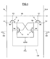
- each memory cell has two inputs E1 and E2 respectively connected on two metallizations adjacent columns BL and BLN, to receive voltages of command for reading and writing the data stored in the memory cell.
- each memory cell is selected by a WL signal carried by a line metallization or "wordline".
- the memory cell CM has two NMOS access transistors, respectively referenced T1 and T2 whose respective grids are connected on the line of word, the corresponding nodes EC thus forming an entry of selection for this memory cell.
- the memory cell CM includes two NMOS storage transistors T3 and T4.
- the storage capacity of the memorized data is formed by the gate / source capacitance of a storage transistor.
- the gate of transistor T4 and the drain of transistor T3 are connected to the drain of the access transistor T1, the corresponding node being referenced B.
- the respective sources and access transistors T1 and T2 are respectively connected to the two control inputs E1 and E2.
- the sources of the two storage transistors T3 and T4 are connected together to a first bias voltage predetermined AGND.
- the substrate BK of each transistor of the memory cell, or else the BK box of this transistor if this one is boxed, is advantageously connected to a second voltage of POL polarization.
- the transistors of the memory cell CM are arranged in a box (or even in a double box) produced within a semiconductor substrate.
- This embodiment has the advantage of offering less leakage of currents, to be less sensitive to "noise" from the substrate, and to be less sensitive to alpha particles.
- the voltages POL and AGND are advantageously chosen so that these voltages verify the following relationship: - VT ⁇ POL - AGND ⁇ 0 in which VT designates the threshold voltage of the transistors.
- the bias voltage AGND is then replaced by the bias voltage AVDD, for example 3 V.
- AVDD bias voltage
- the voltage at node B is equal to VDD - VT while the voltage at BN node is zero.
- the storage transistor T3 is therefore blocked while the storage transistor T4 is on.
- the value "1" logic is therefore stored in the gate-source capacity of the transistor T4. It should be noted here that since the transistor T3 is blocked, the voltage at node B tends to keep its high value (if we do abstraction of course of stray current leaks). Likewise, since transistor T4 is on, the voltage at node BN tends to be maintained at its zero level. Consequently, the skilled person note here the stability character of the memory cell during the writing phase. Then we deactivate the WL signal, the data is then considered written.
- FIG. 2 illustrates the operation of the memory cell in reading.
- the first step is to preload BL and BLN metallizations to a high level of tension, in this case VDD if the precharge circuit includes transistors PMOS or VDD - VT if the precharge circuit has NMOS transistors.
- the WL signal is activated line selection, which makes both passers-by T1 and T2 access transistors.
- the WL signal When the WL signal is activated, it occurs transiently a PC voltage peak at the BN node. It is essential here to avoid this voltage peak being too high and in particular that it is greater than or equal to the threshold voltage of storage transistors so as to prevent transistor T3 from become passing which would then cause the voltage at node B and block transistor T4 to drive ultimately to a loss of the stored information, to a refresh the data in the "wrong way" and by therefore when reading a data of logical value opposite to that which had been previously written.
- W1 and L1 respectively designating the width and length channel of the storage transistors while W2 and L2 designate the channel width and length of the access transistors; the length corresponds to the drain-source distance).
- the duration of the reading cycle of such a memory cell is typically of the order of 30ns while the cooling time information is much shorter, typically on the order of 5ns for a grid / source storage capacity of the order of some fentofarad and stray bit line capacitance of the order of a few hundred fentofarad.
- the structure memory according to the invention advantageously allows the use of specific extremely short refresh cycles.
- the memory cell according to the invention does not require no dedicated manufacturing process for the realization of storage capacitors, and requires only three levels of metallization for its realization in integrated circuit, whereas a memory cell to a transistor requires five levels of metallization.
Landscapes
- Engineering & Computer Science (AREA)
- Microelectronics & Electronic Packaging (AREA)
- Computer Hardware Design (AREA)
- Dram (AREA)
Applications Claiming Priority (2)
| Application Number | Priority Date | Filing Date | Title |
|---|---|---|---|
| FR9712818A FR2769745B1 (fr) | 1997-10-14 | 1997-10-14 | Dispositif de memoire vive dynamique |
| FR9712818 | 1997-10-14 |
Publications (1)
| Publication Number | Publication Date |
|---|---|
| EP0910093A1 true EP0910093A1 (de) | 1999-04-21 |
Family
ID=9512191
Family Applications (1)
| Application Number | Title | Priority Date | Filing Date |
|---|---|---|---|
| EP98402477A Withdrawn EP0910093A1 (de) | 1997-10-14 | 1998-10-06 | Dynamische Speicheranordnung |
Country Status (3)
| Country | Link |
|---|---|
| US (1) | US6177694B1 (de) |
| EP (1) | EP0910093A1 (de) |
| FR (1) | FR2769745B1 (de) |
Families Citing this family (2)
| Publication number | Priority date | Publication date | Assignee | Title |
|---|---|---|---|---|
| US6583459B1 (en) * | 2000-06-30 | 2003-06-24 | Stmicroelectronics, Inc. | Random access memory cell and method for fabricating same |
| JP4038351B2 (ja) * | 2001-05-29 | 2008-01-23 | 株式会社東芝 | 半導体記憶装置 |
Citations (2)
| Publication number | Priority date | Publication date | Assignee | Title |
|---|---|---|---|---|
| US4023149A (en) * | 1975-10-28 | 1977-05-10 | Motorola, Inc. | Static storage technique for four transistor IGFET memory cell |
| EP0681331A2 (de) * | 1994-04-29 | 1995-11-08 | Texas Instruments Incorporated | Verbesserungen in oder an dynamische Speicheranordnungen mit wahlfreiem Zugriff |
-
1997
- 1997-10-14 FR FR9712818A patent/FR2769745B1/fr not_active Expired - Fee Related
-
1998
- 1998-10-06 EP EP98402477A patent/EP0910093A1/de not_active Withdrawn
- 1998-10-13 US US09/170,611 patent/US6177694B1/en not_active Expired - Lifetime
Patent Citations (2)
| Publication number | Priority date | Publication date | Assignee | Title |
|---|---|---|---|---|
| US4023149A (en) * | 1975-10-28 | 1977-05-10 | Motorola, Inc. | Static storage technique for four transistor IGFET memory cell |
| EP0681331A2 (de) * | 1994-04-29 | 1995-11-08 | Texas Instruments Incorporated | Verbesserungen in oder an dynamische Speicheranordnungen mit wahlfreiem Zugriff |
Also Published As
| Publication number | Publication date |
|---|---|
| US6177694B1 (en) | 2001-01-23 |
| FR2769745B1 (fr) | 2000-01-28 |
| FR2769745A1 (fr) | 1999-04-16 |
Similar Documents
| Publication | Publication Date | Title |
|---|---|---|
| FR2774209A1 (fr) | Procede de controle du circuit de lecture d'un plan memoire et dispositif de memoire correspondant | |
| FR2898432A1 (fr) | Cellules memoire en technologie cmos double-grille dotee de transistors a deux grilles independantes | |
| FR2957449A1 (fr) | Micro-amplificateur de lecture pour memoire | |
| FR2650694A1 (fr) | Memoire vive pour machine de traitement de donnees | |
| CN101065809A (zh) | 用于检测薄弱单元的sram测试方法和sram测试配置 | |
| FR2775382A1 (fr) | Procede de controle du rafraichissement d'un plan memoire d'un dispositif de memoire vive dynamique, et dispositif de memoire vive correspondant | |
| FR2654865A1 (fr) | Procede d'ecriture rapide pour tester une memoire a acces aleatoire. | |
| EP3382709B1 (de) | Sram-speicherzelle | |
| FR3070788A1 (fr) | Procede de programmation d’une cellule memoire dram a un transistor et dispositif memoire | |
| EP0689713B1 (de) | Gegen kollisionen von schweren ionen unempfindliche speicherzelle | |
| US7336553B2 (en) | Enhanced sensing in a hierarchical memory architecture | |
| EP0910093A1 (de) | Dynamische Speicheranordnung | |
| EP1168179B1 (de) | Dynamischer Speicher mit redundanten Zellen | |
| EP1465200B1 (de) | Statische Direktzugriffspeicherzelle (SRAM) und Speichereinheit die diese enthält mit extrem niedrigem Leistungsverbrauch | |
| EP0910094B1 (de) | Dynamische Speicheranordnung mit verkürzter Auffrischungszeit und entsprechende Auffrischungsverfahren | |
| EP0897182B1 (de) | Strahlungsunempfindliche statische Speicherzelle | |
| EP0903746B1 (de) | Verfahren und Vorrichtung zum Lesen und Überschreiben einer dynamischen Speicherzelle | |
| FR2810150A1 (fr) | Dispositif de memoire vive dynamique et procede de commande d'un acces en lecture d'une telle memoire | |
| FR2824176A1 (fr) | Procede et dispositif de lecture de cellules de memoire dynamique | |
| EP1103979A1 (de) | Dynamische Speicheranordnung mit wahlfreiem Zugriff (DRAM) sowie entsprechendes Leseverfahren | |
| FR2810782A1 (fr) | Procede de commande d'un acces en lesture d'une memoire vive dynamique et memoire correspondante | |
| FR2976114A1 (fr) | Memoire double port permettant une lecture-ecriture simultanee | |
| FR2829280A1 (fr) | Dispositif de memoire claquable et procede de claquage d'une telle memoire | |
| FR2881564A1 (fr) | Circuit integre de memoire, en particulier de memoire sram et procede de fabrication correspondant | |
| FR2857149A1 (fr) | Procede de commande des amplificateurs de lecture d'une memoire et circuit integre de memoire correspondant |
Legal Events
| Date | Code | Title | Description |
|---|---|---|---|
| PUAI | Public reference made under article 153(3) epc to a published international application that has entered the european phase |
Free format text: ORIGINAL CODE: 0009012 |
|
| AK | Designated contracting states |
Kind code of ref document: A1 Designated state(s): DE FR GB IT |
|
| AX | Request for extension of the european patent |
Free format text: AL;LT;LV;MK;RO;SI |
|
| 17P | Request for examination filed |
Effective date: 19990507 |
|
| AKX | Designation fees paid |
Free format text: DE FR GB IT |
|
| RAP1 | Party data changed (applicant data changed or rights of an application transferred) |
Owner name: STMICROELECTRONICS S.A. |
|
| 17Q | First examination report despatched |
Effective date: 20020905 |
|
| STAA | Information on the status of an ep patent application or granted ep patent |
Free format text: STATUS: THE APPLICATION IS DEEMED TO BE WITHDRAWN |
|
| 18D | Application deemed to be withdrawn |
Effective date: 20030317 |