EP0682347A2 - Widerstand für Telefon - Google Patents
Widerstand für Telefon Download PDFInfo
- Publication number
- EP0682347A2 EP0682347A2 EP95300535A EP95300535A EP0682347A2 EP 0682347 A2 EP0682347 A2 EP 0682347A2 EP 95300535 A EP95300535 A EP 95300535A EP 95300535 A EP95300535 A EP 95300535A EP 0682347 A2 EP0682347 A2 EP 0682347A2
- Authority
- EP
- European Patent Office
- Prior art keywords
- substrate
- cold
- film
- resistive film
- fracture
- Prior art date
- Legal status (The legal status is an assumption and is not a legal conclusion. Google has not performed a legal analysis and makes no representation as to the accuracy of the status listed.)
- Granted
Links
Images


Classifications
-
- H—ELECTRICITY
- H01—ELECTRIC ELEMENTS
- H01C—RESISTORS
- H01C7/00—Non-adjustable resistors formed as one or more layers or coatings; Non-adjustable resistors made from powdered conducting material or powdered semi-conducting material with or without insulating material
- H01C7/10—Non-adjustable resistors formed as one or more layers or coatings; Non-adjustable resistors made from powdered conducting material or powdered semi-conducting material with or without insulating material voltage responsive, i.e. varistors
- H01C7/12—Overvoltage protection resistors; Arresters
-
- H—ELECTRICITY
- H01—ELECTRIC ELEMENTS
- H01H—ELECTRIC SWITCHES; RELAYS; SELECTORS; EMERGENCY PROTECTIVE DEVICES
- H01H85/00—Protective devices in which the current flows through a part of fusible material and this current is interrupted by displacement of the fusible material when this current becomes excessive
- H01H85/0039—Means for influencing the rupture process of the fusible element
- H01H85/0073—Expansion or rupture of the insulating support for the fusible element
-
- H—ELECTRICITY
- H01—ELECTRIC ELEMENTS
- H01H—ELECTRIC SWITCHES; RELAYS; SELECTORS; EMERGENCY PROTECTIVE DEVICES
- H01H85/00—Protective devices in which the current flows through a part of fusible material and this current is interrupted by displacement of the fusible material when this current becomes excessive
- H01H85/02—Details
- H01H85/04—Fuses, i.e. expendable parts of the protective device, e.g. cartridges
- H01H85/041—Fuses, i.e. expendable parts of the protective device, e.g. cartridges characterised by the type
- H01H85/046—Fuses formed as printed circuits
-
- H—ELECTRICITY
- H01—ELECTRIC ELEMENTS
- H01H—ELECTRIC SWITCHES; RELAYS; SELECTORS; EMERGENCY PROTECTIVE DEVICES
- H01H85/00—Protective devices in which the current flows through a part of fusible material and this current is interrupted by displacement of the fusible material when this current becomes excessive
- H01H85/02—Details
- H01H85/04—Fuses, i.e. expendable parts of the protective device, e.g. cartridges
- H01H85/041—Fuses, i.e. expendable parts of the protective device, e.g. cartridges characterised by the type
- H01H85/048—Fuse resistors
Definitions
- This invention relates generally to resistors of the type that fracture in response to high electrical overloads in order to interrupt the current flow through the resistor.
- resistors of the type that fracture in response to high electrical overloads in order to interrupt the current flow through the resistor.
- telephone line balancing telephone line interface resistors that are fracturing resistors.
- a resistor comprises:
- a thermal stress-caused fracture line extends generally away from and/or toward that edge having the terminals, so that the terminals remain effective to hold the ceramic substrate in position on the circuit board and prevent debris dropping onto the board or elsewhere.
- edge of the resistor having the terminals is provided with extra solder that operates as an anchor to reduce further the chances that debris will drop onto the circuit board or elsewhere.
- the fracturing resistors are provided in combination with fusible elements that operate to break the circuit or circuits in situations when the overload is not sufficiently high to cause fracturing.
- frontside heating denote heating of a substrate caused by resistive film actually present on the frontside of the substrate.
- backside heating denote heating of the substrate caused by resistive film actually present on the backside of the substrate.
- a telephone line balancing resistor pair embodying the invention and the method of the invention.
- the most common high electrical overload abuse to which such resistors (in that industry) are subjected results when the most common electrical power distribution voltages accidentally contact the telephone line.
- the most common electrical distribution voltages are 120 volts rmsAC [root mean square alternating current], 208 volts rmsAC, or 230 volts rmsAC.
- the resulting voltage delivered through the telephone line to the balancing resistors causes a substantial overload and consequent fracturing.
- the rmsAC overload voltages present at the resistor, and which cause fracture, are most commonly and typically in the range of about 60 volts rmsAC to about 230 volts rmsAC.
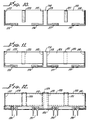
- the balancing resistor pair of Figs. 1-6 has a thin, flat, elongate rectangular substrate 10.
- the thermal coefficient of expansion of substrate 10 is sufficiently high to effect the desired fracturing but not so high that fracturing occurs at excessively low overloads.
- the frontside of substrate 10 there are two screen-printed films (“thick films”) that are serpentine in shape, each film being the mirror image of the other about the CL (vertical center line of the substrate).
- the terminals associated with the films are mirror images about the CL.
- the films and terminals being mirror images, only those at the left side of the CL in Figs. 1, 3 and 5 are described.
- Corresponding elements on the right side of the CL in such figures are given the same reference numerals but followed by the letter "a”.
- the serpentine film is numbered 11 and has its runs extending horizontally, these being numbered 12-17 from top to bottom.
- Top and bottom runs 12 and 17 extend farther to the left than do those between them and are connected by a vertical run 18 that is close to the left end of the substrate.
- the various runs 12-18 are close to each other, and 12-17 are parallel to each other.
- Top run 12 is close to the top edge T of the substrate, but run 16 is spaced from the bottom edge B thereof.
- serpentine film 11 is formed of resistive material, a large amount of frontside heating of substrate 10 is caused by such serpentine film.
- the entire serpentine film 11 is formed of resistive material--with the major exceptions stated below.
- Metalizations 20-26 are corner conductors for serpentine film 11; these greatly increase conductivity at the corners and thereby augment the uniformity of current distribution in the resistive film. Corner conductors 20, 23, and 26 are for right-angle corners, while corner conductors 21, 22, 24, and 25 are for reverse-bent corners.
- cold bars Five of the metalizations, which may be called cold bars, are provided in horizontally-elongate shape and orientation and are in vertical alignment with each other. These are numbered 28-32.
- corner conductors and cold bars are all so located on substrate 10 as to fit into the serpentine pattern of film 11, as shown in Figs. 1 and 5.
- resistive film meaning resistance film having a relatively high resistivity--namely a resistivity which is high relative to the resistivity of the connecting metalization--and that accordingly results in generation of substantial heat in the resistance film when overload current flows through it.
- the resistive film in most instances, extends between the various corner conductors and the cold bars.
- Terminals (terminal pins) 33, 34 are connected by soldering to the metalization pads at the bottom edge B of substrate 10 and are subsequently soldered into holes in line card or circuit board 36 shown in Fig. 1. In the illustrated form, there are two terminals 33 that connect to the same metalization pad 37 on the frontside of the substrate (Fig. 3).
- terminals 33 and their pad 37 are (in the present example) spaced a substantial distance to the right from the left edge of substrate 10. Terminals 34 connect to a blind pad 38 that is spaced to the right from pad 37, these also being soldered into the line card.
- the terminal pins and their mechanical connections to the substrates are preferably stiff, so as to keep the substrate sections vertical before and after fracture occurs.
- the sectional view of Fig. 9a (drawing sheet 3) applies to all of the embodiments set forth in this application--being of the conventional "jaw" type.
- the bottom run 17 of serpentine film 11 is short and at the left end of the substrate, extending along the bottom substrate edge from corner conductor 23 to pad 37.
- An overglaze 40 is provided on the frontside, as indicated in Fig. 1.
- the overglaze is not (except as stated below) present at pads 37, 38, or at the lower edge regions of the substrate inboard of outer terminals 33, nor is it present at other pads described subsequently relative to the central region of the substrate. Despite what is stated in the preceding sentence, there are narrow fingers of overglaze separating the terminal attachments on the pads, as shown.
- fracture (cracking) of substrate 10 is achieved which is reliably and repeatably in generally a particular direction and a particular area.
- the direction is generally or substantially vertical or transverse relative to the bottom edge B of substrate 10, and generally vertical or transverse relative to the top edge T.
- such bottom edge is connected to and supported by the terminals 33, 34 to circuit board or telephone line card 36, so that because the fracture is generally vertical, the pieces of the substrate may therefore not fall onto the circuit board or elsewhere, but instead remain in place.
- the fracture is substantially certain to break the circuit through the film 11 so that the desired "fuse" action is reliably achieved.
- the method is such that the location of the fracture is generally between the cold bars 28-32 and the corner conductors 24, 25 (Fig. 3). Accordingly, the fracture does not normally occur, under the most common high electrical overload abuse conditions, at the left end of the substrate (this being the end outboard of terminals 33). Because of this, and because of additional safety factors relative to certain forms of the method and article, the chances of resistor debris dropping onto the line card or elsewhere are further reduced to a very low percentage.
- the repeatable, substantially vertical fracture is, in accordance with the present method, in the great majority of instances directed toward or away from the terminals (pins) that are electrically and mechanically bonded to the bottom edge of the ceramic and to the line card or circuit board.
- the pieces created by the substantially vertical fracture are then held and may not fall away. (It is pointed out that the direction of propagation of the fracture--whether it starts at the top or bottom or is simultaneous throughout--is irrelevant.)
- the fracture is barely noticeable--being a crack in the ceramic substrate without substantial dimensional separation.
- This crack in the ceramic destroys or greatly damages the support of the resistive film (resistor deposit) which is directly over the crack, thereby causing quick opening (burnout) of the resistor at that location.
- the circuit is thus opened quickly, quick enough not to melt or damage the fine wires which are connected to the telephone system, or cause heat damage to the circuit board due to the heating of the resistors.
- the pattern of frontside cold--meaning relative cold in relation to frontside-heated areas-- is generally U-shaped, with the U opening upwardly and having its base at the bottom edge region of the substrate.
- the phantom line 42 shows the U-shaped cold area (on each side of the CL).
- U-shaped containment of a heat-generating area.
- the heat-generating area defined within the stated U-shaped region--namely, the area between the vertical cold arms of the U--rapidly expands due to the resistor heating and the thermal coefficient of expansion of the ceramic substrate material. This causes increasing strain in the ceramic between the arms of the U due to the thermal contrast in the cold area and the contained, expanding heat-generating area.
- the increasing strain results in the essentially vertical fracture, an example of which is shown at 43 on the left half of the resistor (Fig. 1), and another example is shown at 44 on the right half of such resistor.
- any cold region at the top of the substrate is intentionally made as thin as practical relative to the three sides of the U to thereby reduce greatly the possibility of random breakage as distinguished from generally vertical breakage.
- the size of the heat-generating area is intentionally made sufficiently large to achieve the stated expansion of a relatively large area (proportion) of the substrate.
- each arm of the U is intentionally made sufficiently wide that the cold there maintains sufficient thermal contrast relative to the thermal conductivity of the substrate and will contain the heated expanding ceramic so as to result in sufficient thermal stress to cause the fracture described.
- the region of the substrate to the right of corner bars 24, 25 (Fig. 3), being the right vertical arm of the U, is cold because there is no resistive film over a relatively large area that extends to the CL. (It is to be understood that there is a corresponding cold area to the right of the CL and which relates to the resistive film to the right thereof).
- the left vertical arm of the U is caused by the high-conductivity cold bars 28-32 through which the current flows without generating substantial heat.
- each vertical arm of the U is greater than 0.050 inch (1.25 mm), preferably greater than 0.060 inch (1.5 mm), and in the best embodiment of the method (and article) is about 0.1 inch (2.5mm). In at least the latter instance, the substrate breaks generally vertically at all overload voltages most frequently applied to telephone circuit balancing resistor pairs in telephone system operation.
- the vertical dimension of the base of each cold U is caused to be substantially equal to--or somewhat less than--the horizontal dimension of each arm of the U.
- the heated area continued within the U is generally square; this permits reduction in the widths of the arms (and base) of the U necessary to reliably achieve vertical fracture.
- any backside heating is, at least in the region registered with the U, such as not to interfere with the stated U-shaped containment and consequent desired vertical fracture. Stated otherwise, it does not impact the thermal contrast of the cold frontside U versus the contained heat-generating frontside area.
- One instance (not all-inclusive) where there is (or may be) such interference is where the power density on the backside is so high--at least in the vicinity of the frontside U--as to dominate the thermal effects occurring on the frontside.
- the cold area is V-shaped instead of U-shaped or substantially U-shaped.
- the resistive film within the V is normally serpentine, the runs of which progressively change in length.
- One of the advantages of the present invention is that no horizontal metalization trace is required in spaced relationship above the resistive films, nor are vertical metalization traces required at the substrate ends in spaced relationship from the resistive film. Space is thus saved, and the crack or fracture need not intersect a metalization trace.
- Figs. 2, 4, and 6 there is shown the backside of the resistor described in detail above. Except as specifically stated below, the elements of the right side of the CL in Figs. 2, 4, and 6 are the mirror images of those on the left side thereof, and are accordingly given the same reference numerals except followed in each instance by the letter "b".
- a meandering, serpentine film 46 is illustrated.
- Such film has a vertical pattern at the left end thereof and a horizontal pattern disposed between such vertical pattern and the CL. Because film 46 is formed primarily of resistive material, there is backside heating of the substrate 10 except at the central region of the substrate, and except at the lower portion of the substrate that is below the horizontal film.
- the inboard half of the horizontal film pattern on the backside is substantially registered with that portion of the frontside serpentine pattern that is inboard of cold bars 28-32.
- FIG. 4 showing metalizations, there are vertically-oriented corner conductors 47 for the return-bent corners of the horizontal portion of film 46. There are also horizontally-oriented corner conductors 48 for the return-bent corners of the vertical portion of film 46. There are also corner conductors 49 for the right angle portions of film 46.
- a shunting conductor 51 For trimming and balancing resistance values on the backside, there is a shunting conductor 51 parallel to and outwardly adjacent the uppermost vertical corner conductor 47.
- a U-shaped conductor 52 For more extensive trimming, there is a U-shaped conductor 52, and inboard of which is a vertical conductor 53. These elements 52, 53 are only--in the illustrated embodiment--provided on the left side of the CL as viewed in Fig. 4 but could be on both sides.
- the resistive film is overprinted in the illustrated meandering, serpentine pattern, extending between the various corner conductors 47, 48 and 49.
- the shunting conductor 51 is adapted to be laser cut in order to extend the length, somewhat, of the loop between the second and third (from the top) runs of the horizontal film pattern.
- a trim film 54 is provided between vertical conductor 53 and the right arm of U-shaped conductor 52.
- This film 54 is adapted to be laser-trimmed in a horizontal direction with one or more laser-cut lines in order to effect fine trimming.
- the U-shaped conductor 52 is adapted to be laser-cut in order to introduce into the film pattern that film region lying between the arms of the metalization U.
- the most trimming is effected near the bottom portion of the substrate in order that the heating of the upper portion of the substrate will not be much affected. This is especially true in those instances (not shown here) when laser trimming is provided on the frontside of the substrate instead of the backside thereof.
- the backside films are overprinted with glass 56, except at the lower edge regions (inboard of the outer terminals) and at portions of the middle.
- the backside overglaze 56 is not present along the lower edge portion of substrate 10 except at the outer end thereof where the lowermost run of the meandering serpentine film is present, and except at the indicated (Fig. 2) downwardly-extending fingers between the respective terminals 33, 34, 33a and 34a.
- Pad 61 is blind, while pad 62 connects to the lowermost inboard run portion of the horizontal serpentine film as shown in Fig. 6.
- Each set of terminals or pins connects to the pads on both sides of the substrate.
- terminals 33 connect to pads 37 and 61b; terminals 34 connect to pads 38 and 62b; terminals 34a connect to pads 38a and 62; and terminals 33a connect to pads 37a and 61.
- Fig. 9b drawing sheet 3.
- both vertical fractures will be inboard of the innermost terminals 34 and 34a.
- an extension arm 64 By extending the backside metalization pad 62 inwardly, almost but not quite to the CL, there is provided an extension arm 64. Solder will adhere, when the part is dipped in a molten bath of solder, to any metalization not covered by the glass or overglaze 56 (Fig. 2). It follows that during solder-dipping, not only are the terminals mechanically and electrically connected to their respective pads, but solder 66 is adhered over the extension arms 64 as shown in Fig. 2.
- the solder is ductile and malleable instead of brittle, it does not break when the fracture occurs. Furthermore, there is a meniscus that is formed so that at certain regions, the solder is several thousandths of an inch (several hundredths of a millimetre) thick. Accordingly, the solder provides a bridge across each crack, and this bridge tends to prevent the central region of the resistor from dropping onto the line card. It is pointed out that even a small retaining force is typically effective to prevent such dropping, in that at common overload voltages the ceramic does not break in any major or explosive manner, but instead merely cracks-the facing edge surfaces of the ceramic on opposite sides of each crack being closely adjacent each other.
- Figs. 2, 4 and 6 are exemplary of elements whose backside heating (or absence of it) is such that the functions described under the heading "Description of the Method and of the Operation of the Article as Thus Far Described" are not interfered with.
- the embodiment of Figs. 1-6 operates in the vertical-fracture manner described.
- a phantom line 71 that generally surrounds the cold areas resulting from backside heating of the substrate. These cold areas, and the backside heated areas outside of them, are exemplary of backside cold and heat regions that do not prevent the U-shaped containment described relative to Fig. 1 from operating satisfactorily.
- the front and back resistors on the left side of the CL are connected electrically to each other and combine to form "one resistor" of the resistor pair.
- the front and back resistors on the right side of the CL are connected electrically to each other and form the "other resistor" of the pair.
- Such one resistor and such other resistor are in the great majority of cases caused to have resistances that are equal to each other.
- the resistance on each side of the CL is 50 ohms.
- the front and back resistors on each side of the CL are connected in series with each other.
- the series circuits are through springs next described.
- the connections could be parallel instead of series.
- Pad 72 is blind; pad 73 is connected to metalization 26; and pad 74 is connected to a pad 76 beneath the right end of the uppermost horizontal run of film 46.
- An electrically conductive spring clip 77 is soldered to pad 73 during the above-described dipping process and has an upper end that is soldered to pad 72 and also pad 74--hooking over the upper edge of the substrate. As described in the cited patent, the spring clip 77 is soldered to pad 73 under stressed condition and is accordingly urged outwardly at the lower end thereof on the frontside of the substrate. Thus, when solder melting occurs, as a result of a low overload, the lower end of the frontside spring portion moves outwardly and breaks the circuit.
- FIG. 7 there is shown an elongate substrate 86 for a balanced pair of telephone line resistors.
- the various elements shown in Figs. 7-9 are mirror images about the CL. Thus, only the left resistor is described; the elements on the right side of the CL having the same reference numerals but followed by the letter "a".
- FIG. 8 there is a vertical high-conductivity metalization trace 87 along the left edge of substrate 86 and closely adjacent such edge. There is another metalization trace 88 parallel to trace 87 and spaced to the left of the CL. An H-shaped, high-conductivity metalization trace 89 is located intermediate traces 87, 88, being shown as midway therebetween. The metalization 89 has two vertical legs 91, 92 that are spaced horizontally from each other and connected by a cross-bar 93.
- a first rectangular resistive film 94 is screen-deposited between trace 87 and leg 91, and is also overprinted on such elements.
- a second rectangular resistive film 95 is deposited between leg 92 and trace 88 and overprinted thereon.
- the upper edges of films 94, 95 are closely adjacent the top edge of substrate 86.
- the lower edges of films 94, 95 are spaced upwardly from the bottom edge of the substrate.
- metalization pads 96, 97 are respectively connected to traces 87, 88. They have terminals or pins 98, 99 soldered thereto. As previously stated, Fig. 9a shows terminal or pin 99 and the associated line card, the solder being unshown.
- the resistive films are (in this and subsequently described embodiments) trimmed to the desired resistance value by laser-cut lines (not shown) in the resistive films, extending horizontally and varying in width.
- the backside of the substrate is plain, in the present example, except for blind metalization pads for the soldering of pins 98, 99.
- the base of the indicated U-shaped cold zone is along the bottom edge of the substrate, directly below film 95.
- the resistive films 94, 95 are in series with each other through the crossbar 93, between the pins 98, 99.
- film 95 expands rapidly but is surrounded by the above-described U-shaped cold zone.
- substantially or generally vertical cracks or fractures 104, 105 are formed to break the circuit (circuits) between the various pins.
- the substrate's surface is efficiently used in that the resistive film extends very close to the top edge of the substrate and the end edges thereof.
- an elongate substrate 110 has metalizations 111, 112, 113, 114, 115, 116, 117 and 118 thereon corresponding generally to those shown and described relative to Fig. 8.
- Metalizations 111-114 are for the ends of the resistive films, while metalizations 115-118 are pads for the terminals.
- the backside of substrate 110 is plain, except for metalization pads for connection of the terminals.
- Additional and critical metalizations 120, 121, each vertically elongate, are applied and respectively located intermediate the respective metalizations in each set 111, 112 and 113, 114 thereof.
- Resistive films 122, 123 are applied over all vertically extending metalizations (including 120, 121) as shown in Fig. 11, close to the top of the substrate but spaced from the bottom thereof.
- the adjacent ends of the resistive films are separated from each other by a vertical cold arm 124.
- Metalizations 120, 121 also form vertical cold arms because the current flows through them instead of through the resistive films.
- the metalizations 120, 121 could, alternatively, be applied over the resistive films, but this is not preferred.
- the widths of the arms, and of the base of each U, are intentionally so selected as to cause the vertical fractures.
- An elongate rectangular substrate 140 has (Fig. 13) vertical metalizations (traces) 141, 142, 143 and 144 applied in spaced relationship therealong. These connect, respectively, to pads 145, 146, 147 and 148 for pins 149, 150, 151 and 152 (Fig. 15).
- the central metalizations 142, 143 are preferably in the center of the substrate and are spaced from each other on opposite sides of the CL to form a vertical arm or gap 154.
- Metalizations 141, 144 are respectively spaced from the ends of the substrate to form vertical arms 155, 156.
- Resistive films 158, 159 are provided respectively between metalizations 141-142 and 143-144. These are close to the top of the substrate, but spaced from the bottom thereof.
- each U is substantially equal to or somewhat greater than the vertical dimension of the base of the U.
- Figs. 1-15 there is preferably the same substrate material having the expansion characteristics stated relative to the embodiment of Figs. 1-6.
- This is preferably aluminum oxide, as described in the cited patent.
- the thickness of the thin flat substrate may vary, with the thinner substrates fracturing more rapidly than those less thin. Typical thicknesses are 0.030 inch (0.75 mm), 0.040 inch (1.0 mm), 0.025 inch (0.63 mm), and 0.035 inch (0.88 mm).
- the terminals are mechanically and electrically connected to circuit boards or line cards.
- the illustrated (Figs. 1, 2, 7, 9a, 12 and 15) preferred terminals (terminal pins) are sufficiently stiff to hold the substrates vertical.
- the resistor has a low profile, namely a relatively short height above the circuit board. This is extremely desirable for the telephone line cards.
Landscapes
- Engineering & Computer Science (AREA)
- Microelectronics & Electronic Packaging (AREA)
- Physics & Mathematics (AREA)
- Electromagnetism (AREA)
- Parts Printed On Printed Circuit Boards (AREA)
- Details Of Resistors (AREA)
- Secondary Cells (AREA)
- Electron Tubes For Measurement (AREA)
- Conductive Materials (AREA)
- Telephone Set Structure (AREA)
- Networks Using Active Elements (AREA)
- Input Circuits Of Receivers And Coupling Of Receivers And Audio Equipment (AREA)
Applications Claiming Priority (2)
| Application Number | Priority Date | Filing Date | Title |
|---|---|---|---|
| US08/240,322 US5481242A (en) | 1994-05-10 | 1994-05-10 | Debris-reducing telephone resistor combination and method |
| US240322 | 1994-05-10 |
Publications (3)
| Publication Number | Publication Date |
|---|---|
| EP0682347A2 true EP0682347A2 (de) | 1995-11-15 |
| EP0682347A3 EP0682347A3 (de) | 1996-07-10 |
| EP0682347B1 EP0682347B1 (de) | 1999-03-17 |
Family
ID=22906079
Family Applications (1)
| Application Number | Title | Priority Date | Filing Date |
|---|---|---|---|
| EP95300535A Expired - Lifetime EP0682347B1 (de) | 1994-05-10 | 1995-01-27 | Widerstand für Telefon |
Country Status (7)
| Country | Link |
|---|---|
| US (1) | US5481242A (de) |
| EP (1) | EP0682347B1 (de) |
| JP (1) | JP2635301B2 (de) |
| AT (1) | ATE177870T1 (de) |
| DE (1) | DE69508301T2 (de) |
| ES (1) | ES2128656T3 (de) |
| TW (1) | TW273064B (de) |
Families Citing this family (4)
| Publication number | Priority date | Publication date | Assignee | Title |
|---|---|---|---|---|
| US5594407A (en) * | 1994-07-12 | 1997-01-14 | Caddock Electronics, Inc. | Debris-reducing film-type resistor and method |
| US5914648A (en) * | 1995-03-07 | 1999-06-22 | Caddock Electronics, Inc. | Fault current fusing resistor and method |
| CN100586605C (zh) * | 2007-10-31 | 2010-02-03 | 李世鹏 | 轮圈及轮圈的制造方法 |
| DE102013214194B4 (de) * | 2013-07-19 | 2016-05-04 | Phoenix Contact Gmbh & Co. Kg | Bauraumbegrenzte Überspannungsschutzvorrichtung und Verfahren zu dessen Herstellung |
Family Cites Families (20)
| Publication number | Priority date | Publication date | Assignee | Title |
|---|---|---|---|---|
| SE341746B (de) * | 1970-03-10 | 1972-09-18 | Ericsson Telefon Ab L M | |
| GB1371344A (en) * | 1970-10-17 | 1974-10-23 | Licentia Gmbh | Filter circuit with gyrators and capacitors |
| GB1466569A (en) * | 1973-10-05 | 1977-03-09 | Erie Electronics Ltd | Resistors |
| US4297670A (en) * | 1977-06-03 | 1981-10-27 | Angstrohm Precision, Inc. | Metal foil resistor |
| DE3245629A1 (de) * | 1982-12-09 | 1984-06-14 | Telefunken electronic GmbH, 6000 Frankfurt | Sicherungselement mit einer dickschichtwiderstandsanordnung |
| US4528546A (en) * | 1983-05-02 | 1985-07-09 | National Semiconductor Corporation | High power thick film |
| US4467310A (en) * | 1983-10-03 | 1984-08-21 | Northern Telecom Limited | Telephone subscriber line battery feed resistor arrangements |
| FR2562711B1 (fr) * | 1984-04-10 | 1987-01-23 | Renix Electronique Sa | Resistance haute tension de precision a faible encombrement en technologie couches epaisses |
| GB2163307B (en) * | 1984-08-15 | 1987-12-16 | Crystalate Electronics | Fusible electrical resistor |
| US4809324A (en) * | 1987-07-27 | 1989-02-28 | Siemens Transmission Systems, Inc. | Subscriber line interface circuit (SLIC) isolation from lighting-induced ground overshoots |
| JPH01220403A (ja) * | 1988-02-26 | 1989-09-04 | Murata Mfg Co Ltd | ケース内蔵型の正特性サーミスタ |
| US4959751A (en) * | 1988-08-16 | 1990-09-25 | Delco Electronics Corporation | Ceramic hybrid integrated circuit having surface mount device solder stress reduction |
| US4961065A (en) * | 1989-03-27 | 1990-10-02 | Cts Corporation | Fail-safe resistor |
| GB2230921B (en) * | 1989-04-25 | 1994-01-05 | Plessey Telecomm | Protective arrangement for telecommunications line interface circuit |
| US5204799A (en) * | 1990-03-22 | 1993-04-20 | Gpt Limited | Protective arrangement for telecommunications line interface circuit |
| US5254969A (en) * | 1991-04-02 | 1993-10-19 | Caddock Electronics, Inc. | Resistor combination and method |
| EP0507465B1 (de) * | 1991-04-02 | 1998-12-02 | Caddock Electronics, Inc. | Widerstand, der imstande ist, als Überlastschalter zu agieren |
| EP0508615B1 (de) * | 1991-04-10 | 1997-07-02 | Caddock Electronics, Inc. | Schichtwiderstand |
| US5252944A (en) * | 1991-09-12 | 1993-10-12 | Caddock Electronics, Inc. | Film-type electrical resistor combination |
| US5404126A (en) * | 1992-09-15 | 1995-04-04 | Okaya Electric Industries Co., Ltd. | Fuse Resistor, and discharging-type surge absorbing device with security mechanism |
-
1994
- 1994-05-10 US US08/240,322 patent/US5481242A/en not_active Expired - Lifetime
- 1994-10-03 TW TW083108051A patent/TW273064B/zh not_active IP Right Cessation
- 1994-12-21 JP JP6318780A patent/JP2635301B2/ja not_active Expired - Fee Related
-
1995
- 1995-01-27 DE DE69508301T patent/DE69508301T2/de not_active Expired - Lifetime
- 1995-01-27 ES ES95300535T patent/ES2128656T3/es not_active Expired - Lifetime
- 1995-01-27 AT AT95300535T patent/ATE177870T1/de not_active IP Right Cessation
- 1995-01-27 EP EP95300535A patent/EP0682347B1/de not_active Expired - Lifetime
Also Published As
| Publication number | Publication date |
|---|---|
| EP0682347B1 (de) | 1999-03-17 |
| JPH07307209A (ja) | 1995-11-21 |
| EP0682347A3 (de) | 1996-07-10 |
| DE69508301T2 (de) | 1999-07-15 |
| TW273064B (de) | 1996-03-21 |
| US5481242A (en) | 1996-01-02 |
| ES2128656T3 (es) | 1999-05-16 |
| ATE177870T1 (de) | 1999-04-15 |
| DE69508301D1 (de) | 1999-04-22 |
| JP2635301B2 (ja) | 1997-07-30 |
Similar Documents
| Publication | Publication Date | Title |
|---|---|---|
| US3978443A (en) | Fusible resistor | |
| US4494104A (en) | Thermal Fuse | |
| CN1327467C (zh) | 熔断器件及其制造方法 | |
| EP0649562B1 (de) | Schaltungsschutzeinrichtung | |
| US5057811A (en) | Electrothermal sensor | |
| NZ314160A (en) | Components mounted to printed circuit board by soldering into contoured grooves | |
| US5793274A (en) | Surface mount fusing device | |
| EP0682347B1 (de) | Widerstand für Telefon | |
| US5254969A (en) | Resistor combination and method | |
| US5204799A (en) | Protective arrangement for telecommunications line interface circuit | |
| GB2205455A (en) | Thermal fuse | |
| CA2255587A1 (en) | Thermally fused resistor | |
| US5594407A (en) | Debris-reducing film-type resistor and method | |
| JP2005510079A (ja) | サージ電流チップ抵抗 | |
| US5361300A (en) | Balancing resistor and thermistor network for telephone circuits, and combination thereof with relay | |
| EP0395231B1 (de) | Schutzanordnung für eine Leitungsschnittstellenschaltung einer Fernmeldeanlage | |
| US5581227A (en) | Hybrid circuit having ceramic strip to increase loading capacity | |
| JPH1196886A (ja) | チップ形ヒューズ及びその製造方法 | |
| JP7606842B2 (ja) | シャント抵抗装置、および電流検出用シャント抵抗装置の特性調整方法 | |
| EP0507465B1 (de) | Widerstand, der imstande ist, als Überlastschalter zu agieren | |
| CN211507558U (zh) | 具有金属线型导电熔丝的芯片型保险丝 | |
| JPH0714940A (ja) | ハイブリッドic | |
| JPH0230144Y2 (de) | ||
| JPH074761Y2 (ja) | ヒューズ抵抗器 | |
| JPH10209618A (ja) | 回路基板装置及びその製造方法 |
Legal Events
| Date | Code | Title | Description |
|---|---|---|---|
| PUAI | Public reference made under article 153(3) epc to a published international application that has entered the european phase |
Free format text: ORIGINAL CODE: 0009012 |
|
| AK | Designated contracting states |
Kind code of ref document: A2 Designated state(s): AT BE CH DE DK ES FR GB GR IE IT LI NL PT SE |
|
| PUAL | Search report despatched |
Free format text: ORIGINAL CODE: 0009013 |
|
| AK | Designated contracting states |
Kind code of ref document: A3 Designated state(s): AT BE CH DE DK ES FR GB GR IE IT LI NL PT SE |
|
| 17P | Request for examination filed |
Effective date: 19970103 |
|
| GRAG | Despatch of communication of intention to grant |
Free format text: ORIGINAL CODE: EPIDOS AGRA |
|
| 17Q | First examination report despatched |
Effective date: 19980227 |
|
| GRAG | Despatch of communication of intention to grant |
Free format text: ORIGINAL CODE: EPIDOS AGRA |
|
| GRAH | Despatch of communication of intention to grant a patent |
Free format text: ORIGINAL CODE: EPIDOS IGRA |
|
| GRAH | Despatch of communication of intention to grant a patent |
Free format text: ORIGINAL CODE: EPIDOS IGRA |
|
| GRAA | (expected) grant |
Free format text: ORIGINAL CODE: 0009210 |
|
| AK | Designated contracting states |
Kind code of ref document: B1 Designated state(s): AT BE CH DE DK ES FR GB GR IE IT LI NL PT SE |
|
| PG25 | Lapsed in a contracting state [announced via postgrant information from national office to epo] |
Ref country code: LI Free format text: LAPSE BECAUSE OF FAILURE TO SUBMIT A TRANSLATION OF THE DESCRIPTION OR TO PAY THE FEE WITHIN THE PRESCRIBED TIME-LIMIT Effective date: 19990317 Ref country code: GR Free format text: LAPSE BECAUSE OF NON-PAYMENT OF DUE FEES Effective date: 19990317 Ref country code: CH Free format text: LAPSE BECAUSE OF FAILURE TO SUBMIT A TRANSLATION OF THE DESCRIPTION OR TO PAY THE FEE WITHIN THE PRESCRIBED TIME-LIMIT Effective date: 19990317 Ref country code: BE Free format text: LAPSE BECAUSE OF FAILURE TO SUBMIT A TRANSLATION OF THE DESCRIPTION OR TO PAY THE FEE WITHIN THE PRESCRIBED TIME-LIMIT Effective date: 19990317 Ref country code: AT Free format text: LAPSE BECAUSE OF FAILURE TO SUBMIT A TRANSLATION OF THE DESCRIPTION OR TO PAY THE FEE WITHIN THE PRESCRIBED TIME-LIMIT Effective date: 19990317 |
|
| REF | Corresponds to: |
Ref document number: 177870 Country of ref document: AT Date of ref document: 19990415 Kind code of ref document: T |
|
| REG | Reference to a national code |
Ref country code: CH Ref legal event code: EP |
|
| REG | Reference to a national code |
Ref country code: IE Ref legal event code: FG4D |
|
| REF | Corresponds to: |
Ref document number: 69508301 Country of ref document: DE Date of ref document: 19990422 |
|
| REG | Reference to a national code |
Ref country code: ES Ref legal event code: FG2A Ref document number: 2128656 Country of ref document: ES Kind code of ref document: T3 |
|
| ITF | It: translation for a ep patent filed | ||
| PG25 | Lapsed in a contracting state [announced via postgrant information from national office to epo] |
Ref country code: PT Free format text: LAPSE BECAUSE OF FAILURE TO SUBMIT A TRANSLATION OF THE DESCRIPTION OR TO PAY THE FEE WITHIN THE PRESCRIBED TIME-LIMIT Effective date: 19990617 Ref country code: DK Free format text: LAPSE BECAUSE OF FAILURE TO SUBMIT A TRANSLATION OF THE DESCRIPTION OR TO PAY THE FEE WITHIN THE PRESCRIBED TIME-LIMIT Effective date: 19990617 |
|
| ET | Fr: translation filed | ||
| REG | Reference to a national code |
Ref country code: CH Ref legal event code: PL |
|
| PLBE | No opposition filed within time limit |
Free format text: ORIGINAL CODE: 0009261 |
|
| STAA | Information on the status of an ep patent application or granted ep patent |
Free format text: STATUS: NO OPPOSITION FILED WITHIN TIME LIMIT |
|
| PG25 | Lapsed in a contracting state [announced via postgrant information from national office to epo] |
Ref country code: IE Free format text: LAPSE BECAUSE OF NON-PAYMENT OF DUE FEES Effective date: 20000127 |
|
| 26N | No opposition filed | ||
| REG | Reference to a national code |
Ref country code: IE Ref legal event code: MM4A |
|
| REG | Reference to a national code |
Ref country code: GB Ref legal event code: IF02 |
|
| PGFP | Annual fee paid to national office [announced via postgrant information from national office to epo] |
Ref country code: ES Payment date: 20030218 Year of fee payment: 9 |
|
| PG25 | Lapsed in a contracting state [announced via postgrant information from national office to epo] |
Ref country code: ES Free format text: LAPSE BECAUSE OF NON-PAYMENT OF DUE FEES Effective date: 20040128 |
|
| PG25 | Lapsed in a contracting state [announced via postgrant information from national office to epo] |
Ref country code: IT Free format text: LAPSE BECAUSE OF NON-PAYMENT OF DUE FEES Effective date: 20050127 |
|
| REG | Reference to a national code |
Ref country code: ES Ref legal event code: FD2A Effective date: 20040128 |
|
| PGFP | Annual fee paid to national office [announced via postgrant information from national office to epo] |
Ref country code: NL Payment date: 20110117 Year of fee payment: 17 Ref country code: FR Payment date: 20110128 Year of fee payment: 17 Ref country code: DE Payment date: 20110119 Year of fee payment: 17 Ref country code: SE Payment date: 20110111 Year of fee payment: 17 |
|
| PGFP | Annual fee paid to national office [announced via postgrant information from national office to epo] |
Ref country code: GB Payment date: 20110126 Year of fee payment: 17 |
|
| REG | Reference to a national code |
Ref country code: NL Ref legal event code: V1 Effective date: 20120801 |
|
| REG | Reference to a national code |
Ref country code: SE Ref legal event code: EUG |
|
| GBPC | Gb: european patent ceased through non-payment of renewal fee |
Effective date: 20120127 |
|
| REG | Reference to a national code |
Ref country code: FR Ref legal event code: ST Effective date: 20120928 |
|
| PG25 | Lapsed in a contracting state [announced via postgrant information from national office to epo] |
Ref country code: DE Free format text: LAPSE BECAUSE OF NON-PAYMENT OF DUE FEES Effective date: 20120801 Ref country code: GB Free format text: LAPSE BECAUSE OF NON-PAYMENT OF DUE FEES Effective date: 20120127 Ref country code: SE Free format text: LAPSE BECAUSE OF NON-PAYMENT OF DUE FEES Effective date: 20120128 |
|
| REG | Reference to a national code |
Ref country code: DE Ref legal event code: R119 Ref document number: 69508301 Country of ref document: DE Effective date: 20120801 |
|
| PG25 | Lapsed in a contracting state [announced via postgrant information from national office to epo] |
Ref country code: FR Free format text: LAPSE BECAUSE OF NON-PAYMENT OF DUE FEES Effective date: 20120131 |
|
| PG25 | Lapsed in a contracting state [announced via postgrant information from national office to epo] |
Ref country code: NL Free format text: LAPSE BECAUSE OF NON-PAYMENT OF DUE FEES Effective date: 20120801 |