EP0682360A2 - Verfahren zur Herstellung eines Kondensators aus einer Polysiliziumschicht - Google Patents
Verfahren zur Herstellung eines Kondensators aus einer Polysiliziumschicht Download PDFInfo
- Publication number
- EP0682360A2 EP0682360A2 EP95302951A EP95302951A EP0682360A2 EP 0682360 A2 EP0682360 A2 EP 0682360A2 EP 95302951 A EP95302951 A EP 95302951A EP 95302951 A EP95302951 A EP 95302951A EP 0682360 A2 EP0682360 A2 EP 0682360A2
- Authority
- EP
- European Patent Office
- Prior art keywords
- phosphorous
- depth
- ions
- polysilicon layer
- silicon nitride
- Prior art date
- Legal status (The legal status is an assumption and is not a legal conclusion. Google has not performed a legal analysis and makes no representation as to the accuracy of the status listed.)
- Withdrawn
Links
Images


Classifications
-
- H—ELECTRICITY
- H10—SEMICONDUCTOR DEVICES; ELECTRIC SOLID-STATE DEVICES NOT OTHERWISE PROVIDED FOR
- H10B—ELECTRONIC MEMORY DEVICES
- H10B12/00—Dynamic random access memory [DRAM] devices
- H10B12/01—Manufacture or treatment
- H10B12/02—Manufacture or treatment for one transistor one-capacitor [1T-1C] memory cells
- H10B12/03—Making the capacitor or connections thereto
- H10B12/033—Making the capacitor or connections thereto the capacitor extending over the transistor
-
- H—ELECTRICITY
- H10—SEMICONDUCTOR DEVICES; ELECTRIC SOLID-STATE DEVICES NOT OTHERWISE PROVIDED FOR
- H10B—ELECTRONIC MEMORY DEVICES
- H10B12/00—Dynamic random access memory [DRAM] devices
- H10B12/30—DRAM devices comprising one-transistor - one-capacitor [1T-1C] memory cells
- H10B12/31—DRAM devices comprising one-transistor - one-capacitor [1T-1C] memory cells having a storage electrode stacked over the transistor
-
- H—ELECTRICITY
- H10—SEMICONDUCTOR DEVICES; ELECTRIC SOLID-STATE DEVICES NOT OTHERWISE PROVIDED FOR
- H10D—INORGANIC ELECTRIC SEMICONDUCTOR DEVICES
- H10D1/00—Resistors, capacitors or inductors
- H10D1/60—Capacitors
- H10D1/68—Capacitors having no potential barriers
- H10D1/692—Electrodes
- H10D1/711—Electrodes having non-planar surfaces, e.g. formed by texturisation
-
- H—ELECTRICITY
- H10—SEMICONDUCTOR DEVICES; ELECTRIC SOLID-STATE DEVICES NOT OTHERWISE PROVIDED FOR
- H10D—INORGANIC ELECTRIC SEMICONDUCTOR DEVICES
- H10D1/00—Resistors, capacitors or inductors
- H10D1/60—Capacitors
- H10D1/68—Capacitors having no potential barriers
- H10D1/692—Electrodes
- H10D1/711—Electrodes having non-planar surfaces, e.g. formed by texturisation
- H10D1/712—Electrodes having non-planar surfaces, e.g. formed by texturisation being rough surfaces, e.g. using hemispherical grains
-
- Y—GENERAL TAGGING OF NEW TECHNOLOGICAL DEVELOPMENTS; GENERAL TAGGING OF CROSS-SECTIONAL TECHNOLOGIES SPANNING OVER SEVERAL SECTIONS OF THE IPC; TECHNICAL SUBJECTS COVERED BY FORMER USPC CROSS-REFERENCE ART COLLECTIONS [XRACs] AND DIGESTS
- Y10—TECHNICAL SUBJECTS COVERED BY FORMER USPC
- Y10S—TECHNICAL SUBJECTS COVERED BY FORMER USPC CROSS-REFERENCE ART COLLECTIONS [XRACs] AND DIGESTS
- Y10S148/00—Metal treatment
- Y10S148/014—Capacitor
-
- Y—GENERAL TAGGING OF NEW TECHNOLOGICAL DEVELOPMENTS; GENERAL TAGGING OF CROSS-SECTIONAL TECHNOLOGIES SPANNING OVER SEVERAL SECTIONS OF THE IPC; TECHNICAL SUBJECTS COVERED BY FORMER USPC CROSS-REFERENCE ART COLLECTIONS [XRACs] AND DIGESTS
- Y10—TECHNICAL SUBJECTS COVERED BY FORMER USPC
- Y10S—TECHNICAL SUBJECTS COVERED BY FORMER USPC CROSS-REFERENCE ART COLLECTIONS [XRACs] AND DIGESTS
- Y10S438/00—Semiconductor device manufacturing: process
- Y10S438/964—Roughened surface
Definitions
- This invention relates to integrated circuit manufacture. We will describe a capacitor with enhanced area and dielectric formed by implantation of conductive and insulative layers within a polysilicon material.
- a capacitor is an electronic component capable of storing electrical energy.
- a capacitor consists of two conductive plates insulated from each other by a dielectric.
- Capacitors can be configured in many ways.
- the plates and adjacent dielectrics can take on a planar shape, a trenched shape, a stacked shape or a fin shape.
- a planar capacitor entails a dielectric placed between a pair of planar conductors, wherein the conductors can be polysilicon and/or silicon.
- the polysilicon and silicon are generally formed on or near the substrate topography.
- Each side of the plate is electrically connected to other active devices formed upon the substrate to complete the connection.
- capacitors are sometimes laid out in a trench such that the insulative and conductive regions extend into the substrate instead of across the substrate.
- a trench capacitor thereby occupies a substrate area roughly equal to the thickness of the dielectric and adjoining plates rather than the area of the plates.
- capacitor Another way in which to conserve substrate area is to stack the capacitor on top of the transistors to which they are connected. Stacking of capacitors was favorably introduced in DRAM applications where conservation of area is crucial. It is understood that “capacitor” set forth herein below comprises electrically conductive plates spaced from each other by an insulative material, wherein the plates and insulative material are arranged in a planar, trenched or stacked configuration.
- capacitance value C indicates that in order to increase the capacitance, dielectric constant k and/or area A must be increased or, conversely, thickness t must be decreased.
- a majority of plated capacitors utilize silicon nitride as a preferred dielectric material. Silicon nitride is generally deposited from a chemical vapor deposition (CVD) chamber onto the lower conductive plate. The CVD reaction used for preparing high-temperature silicon nitride is as follows: 3SiH4+NHa--+SiaN4+12H2. Silicon nitride is relatively impermeable to oxygen (as well as phosphorous and boron) and provides an efficient barrier against diffusion between the plates.
- silicon nitride has a dielectric constant K much higherthan, for example, silicon dioxide. While silicon nitride is the preferred dielectric, silicon nitride often exhibits numerous pinholes which may or may not extend through the nitride. Regardless of the CVD techniques used, silicon nitride remains more prone to pinholes that other dielectrics. Pinholes, resulting from deposition, must be avoided in order to ensure the conductive plates do not short to one another.
- conventional capacitors utilize four deposition steps: a first conductive deposition step, followed by an insulative deposition step, followed by a wet oxide step, followed by a second conductive deposition step. All four steps require two separate masking and photolithography steps thereby adding to the complexity of the manufacturing process.
- the plated structure results in a relatively thick combination of conductive and insulative layers which, if placed on an even substrate surfaee, substantially adds to the unevenness of the circuit topography. Subsequent planarization steps involving selective removal of overlaying oxide and/or application of spin-on glass (SOG) are needed to re-planarize the upper surface.
- SOG spin-on glass
- capacitance C can be increased by increasing area A.
- Recent work has been performed in the area of texturization, in which additional area is provided at the juncture between the insulative layer and one of the adjacent conductive layers.
- the conductive layer can be texturized after it has been deposited by growing a sacrificial oxide upon the upper surface of the conductive (generally polysilicon) layer. Doping of the underlying polysilicon prior to oxide growth enhances oxide growth rate and, when performed at a specific temperature, leads to a roughness or texture in the areas at which oxide is grown.
- Oxide grown upon the exposed surface of the deposited polysilicon is then removed leaving a roughened or textured upper surface on which silicon nitride is subsequently placed.
- the method of polysilicon texturization to enhance capacitor surface area is well studied and set forth in U.S. Patent Nos. 5,043,780 to Fazan, et al.; 5,082,797 to Ghan, et al.; 5,102,832 to Tuttle; 5,138,411 to Sandhu; 5,191,509 to Wen; and 5,208,176 to Ahmad, et al. All of the above teach the importance of texturization, but in the context of depositing a polysilicon layer to be textured followed by deposition of a dielectric and another polysilicon thereover.
- a second conductive layer of phosphorous is implanted adjacent the nitrogen layer and opposite the first conductive layer to complete the plated capacitor structure.
- the capacitor is activated by annealing phosphorous atoms and the nitrogen atoms toward silicon atoms.
- nitrogen atoms Proper placement of nitrogen atoms within the polysilicon bulk allows more precise control over the thickness of the ensuing silicon nitride dielectric and also ensures that silicon nitride extends along the entire region between the phosphorous layers in a uniform manner.
- silicon nitride (from a nitrogen implant source) can be relatively thin and substantially void of pinholes and contamination often encountered in conventional non-implanted, layer-by-layer deposition techniques. Further, conventional wet oxidation step, masks, etc.
- a method forfabricating a capacitor comprising the steps of forming an upper surface topography upon a semiconductor substrate and thereafter depositing a polysilicon layer upon the upper surface topography.
- a first plurality of phosphorous ions are then implanted into the polysilicon layer to a concentration peak density at a first depth relative to the upper surface of the polysilicon layer.
- the first plurality of polysilicon ions are implanted at a beam energy sufficient to amorphize a region of the polysilicon layer to a depth greater than the first depth.
- a plurality of nitrogen atoms are then implanted into the polysilicon layer to a concentration peak density at a second depth relative to the upper surface of the polysilicon layer.
- the second depth is less than the first depth, and the nitrogen ions are implanted only within the amorphized region to prevent channelling of the nitrogen ions to a depth equal to or less than the first depth.
- a second plurality of polysilicon ions are then implanted into the polysilicon layer to a concentration peak density at a third depth relative to the upper surface of the polysilicon layer.
- the third depth is less than the second depth, and the second plurality of phosphorous ions are implanted only within the amorphized region to prevent channelling of the second plurality of phosphorous ions to a depth equal to or greater than the second depth.
- the polysilicon layer is then annealed to form a capacitor comprising an insulative silicon nitride layer of implanted nitrogen ions combined with silicon atoms and configured between a conductive first and second phosphorous layer of respective implanted first and second plurality of phosphorous ions.
- a juncture between the silicon nitride layer and both phosphorous layers are textured as a result of diffusion of silicon nitride and phosphorous across the juncture and, further, wherein the silicon nitride occupies diffusion sites within the conductive silicon nitride layer such that electrically conductive paths within the silicon nitride are substantially eliminated.
- the upper surface topography is formed by growing a field oxide and a gate oxide upon the substrate, depositing a conductor upon the field and gate oxides, and depositing a dielectric upon the conductor.
- the dielectric may include oxide formed on the substrate upper surface as well as polysilicon upper surface to electrically separate the polysilicon conductor from the overlying capacitor.
- the annealing step generally includes the steps of subjecting the polysilicon layer to a temperature exceeding 600° C and for a time period exceeding several seconds. Resulting from the heating of the polysilicon layer, the amorphize region recrystallizes and the combination of nitrogen and silicon atoms diffuse across the juncture. Moreover, nitrogen combines with silicon atoms to form silicon nitride having a dielectric constant greater than 3.0. Diffusion across the juncture allows for a texturized interface and provides enhanced surface area of the capacitor. Still further, the silicon nitride insulative layer is substantially free of conductive paths or pinholes between the adjacent conductive layers. By implanting the dielectric rather than depositing it, the dielectric is virtually free of pinholes and has a suitable dielectric constant.
- Fig. 1 is a cross-sectional view of a semiconductor substrate 10, upon which an upper surface topography 12 is formed.
- Substrate 10 can be either n-type or p-type and can include various reverse-doped well regions known in MOS or bipolar technologies.
- Topography 12 includes at least one field oxide region 14 and at least one gate oxide region 16. Deposited upon field and gate oxide 14 and 16, respectively, are conductors 18.
- Conductors 18 can be made of any conductive material, including polycrystalline (polysilicon). Conductors 18 in active regions form a template for implanting self- aligned source/drain or emitter/collector regions 20.
- Upper surface topography 12 contains many peaks and valleys upon which subsequent layers are deposited. The peaks and valleys may lend to extreme disparities in the planarization of the upper surface. Rather than having to deposit numerous layers and, in some instances, relatively thin layers upon the upper surface, only one relatively thick polysilicon layer 22 is deposited according to the present invention, as shown Fig. 2.
- Polysilicon layer 22 is according to an exemplary embodiment approximately 1000 Angstroms thick and is deposited according to chemical vapor deposition (CVD) techniques. In order to maintain relatively small grain size, CVD occurs within a chamber heated at approximately 500° C to 600° C. An appropriate temperature is selected in order to minimize grain size but shall not be so small as would substantially increase the resistivity of polysilicon 22. As shown in Fig. 2, polysilicon 22 is deposited across the entire surface of topography 12 and is insulated from conductors 18 by a previously grown oxide layer 24.
- CVD chemical vapor deposition
- a subsequent processing step is shown, whereby the upper surface polysilicon 22 receives a first plurality of phosphorous ions P 1 .
- Phosphorous ions P 1 are implanted from an ion implanter, preferably a medium to very low energy implanter.
- Phosphorous ions P 1 are implanted using plasma immersion implantation techniques generally described in Cheung, "Plasma immersion ion implantation for ULSI processing.” Trends & Applications, 1991, pp. 811-820 (herein incorporated by reference). Plasma immersion implantation allows for even implantation at areas perpendicular to substrate 10 as well as areas which are angled relative to substrate 10, as shown by arrows 26.
- phosphorous ions P 1 are implanted evenly along the uneven polysilicon layer 22.
- the phosphorous ions are accelerated at a beam current and time period selected such that the implanted ions achieve a dose within polysilicon 22 equal to or greater than approximately 1x10 15 atoms/cm 2 .
- phosphorous ions are implanted at an energy of approximately 40 keV such that the ions are implanted within polysilicon 22 at a first depth 28 of approximately 520 Angstroms relative to the upper surface of polysilicon 22.
- the "upper surface" of polysilicon is defined as the surface upon which the implanted ions initially strike the polysilicon.
- the upper surface includes the exposed upper surface, regardless of whether the exposed surface is parallel with or arranged at an angle with substrate 10.
- Phosphorous ions P 1 are necessary to implant dopant atoms into polysilicon 22.
- the minority carriers are subsequently activated by an anneal step described herein below.
- a subsequent processing step shown in Fig. 4, is needed to form an insulative layer adjacent to the previously deposited phosphorous layer.
- Fig. 4 illustrates a cross-sectional view of polysilicon 22 configured to receive nitrogen ions N. Nitrogen ions are implanted according to plasma immersion techniques to a fairly high dosage in order to subsequently bring about a combination with silicon atoms at the implant sites, wherein the combination of silicon and nitride form silicon nitride in stoichiometric or near stoichiometric proportions.
- nitrogen ions are implanted at a dose of approximately 5x10 15 atoms/cm 2 and at an implant energy of 2.4 keV.
- the implant energy is chosen such that a concentration peak density of the implanted nitrogen is at a second depth 30 relative to the upper surface polysilicon 22.
- the peak concentration appears approximately equal to 3.9x10 23 cm- 3 , and ARp is approximately equal to 51 Angstroms.
- Second depth 30 is approximately 80 Angstroms, as measured from the upper surface, and is less than the first depth 28.
- a second plurality of phosphorous ions P 2 are implanted into polysilicon 22 to a third depth 32, as shown in Fig. 5.
- Phosphorous ions P 2 similar to phosphorous P 1 and nitrogen ions N, are implanted according to plasma immersion techniques to ensure uniform implantation within polysilicon 22 regardless of the angle of implantation or the upper surface configuration of the target surface.
- Phosphorous ions P 2 are implanted at a dose of approximately J X 10 13 atoms/cm 2 and at an implant energy of 0.5 keV. The implant energy is chosen such that the concentration peak density at third depth 32 is approximately at a depth of 22 Angstroms as measured from the upper surface of polysilicon 22.
- first depth 28 is less than second depth 30, and second depth 30 is less than third depth 32.
- first depth 28 is less than second depth 30, and second depth 30 is less than third depth 32.
- a graph of ion concentration verses depth for the first plurality of phosphorous ions P 1 is shown.
- Phosphorous ions P 1 are implanted at a concentration peak density 34 corresponding to first depth 28.
- Depth 28 (often referred to as “range,” or “R") is determined by incremental energy loss resulting from nuclear S n and electronic S c stopping power. Projected range is characterized by its mean value (centered at the maximum concentration point) as well as by the standard deviation, or ARp, along the direction of the incident ion. The latter term of standard deviation is sometimes characterized as "straggle". In general, the standard deviation decreases as the implant energy increases and as the atomic number of the implanted species increases.
- lighter ions have a larger relative dispersion at low energies than heavy ions.
- Phosphorous being a heavier ion than nitrogen, will thereby display a lesser standard deviation than nitrogen. Nonetheless, the concentration curve density for phosphorous ions P 1 shown in Fig. 6, are not entirely Gaussian. Instead, a tail 36 will exist evidencing ion straggle in the forward direction of implant. Ion straggle in the forward direction is often characterized as ion "channeling". Channeling is a well known phenomena and results from the steering of ions through the semiconductor lattice along -areas where energy loss is minimum. Channeled beams result in greatly increased penetration depth as illustrated by tail 36.
- Channeling is prevalent whenever ions are implanted into a single crystal lattice or into a polycrystalline lattice. After the lattice is amorphized or "preamorphized” channeling becomes less prevalent since there is no defined pattern through which the ions can be channeled. High energy implantation of first plurality of phosphorous ions P 1 amorphizes or "preamorphizes" the lattice structure in the cross-hatched area 38. Amorphized region 38 is thereafter advantageously used to prevent or substantial minimize channelling and any tail effects therefrom whenever subsequent implantation occurs.
- a graph of ion concentration verses depth for the first and second plurality of phosphorous ions P 1 and P 2 as well as the plurality of nitrogen ions N are shown.
- High energy implantation of phosphorous ions P, to first depth 28 forms an amorphized region 38 in which subsequent ions of nitrogen N and phosphorous P 2 are implanted.
- Nitrogen ions are implanted at a concentration peak density at second depth 30, which is less than the first depth 28.
- phosphorous ions P 2 are implanted at a concentration peak density at a third depth 32 less than respective second and first depths 30 and 28.
- An important advantage of the embodiment is implantation of nitrogen necessary to form a thin dielectric layer centered about second depth 30.
- Nitrogen ions N are implanted in amorphized region 38 such that little if any channeling or tail affects occur.
- the edge or deepest part of implantation is substantially less for the implanted nitrogen ions than it would be if the nitrogen were implanted in a non- preamorphized polysilicon.
- nitrogen does not experience a tail 40, as shown in Fig. 7 in phantom.
- tail 36 formed by P 1 implant into non-preamorphized polysilicon there is substantially no tail of nitrogen and phosphorous P 2 implanted in amorphous region 38.
- Absence of a tail in subsequently implanted nitrogen N and phosphorous P 2 ensures a fine line demarcation between the implanted regions such that the implanted regions do not overlap one another. It is important that the implanted regions which form the insulative and conductive layers be separate from one another in order that subsequent anneal not lessen the conductive and insulative properties of the ensuing layers.
- an annealing step is used to recrystallize the amorphous region 38 and to anneal out lattice damage caused by the implantation step.
- the composite (implanted) polysilicon layer 22 takes on capacitor characterizes. Namely, the implanted phosphorous ions P 1 and P 2 become electrically active and become conductive when current is applied via, e.g., a metal layer44 contacted therewith. High concentrations of nitrogen atoms in and around second depth 30 combine with silicon atoms to form a silicon nitride of stoichiometric or nearly stoichiometric proportions.
- the silicon nitride is derived from implantation, it achieves the same advantages of deposited thin film silicon nitride.
- implanted silicon nitride is void of pinholes often present in conventional silicon nitride layers.
- the nitride can be implanted with very small standard deviation to achieve an extremely thin silicon nitride layer.
- the silicon nitride layer can, in the present instance be 50 angstroms or less in thickness. By minimizing channeling or tailing of the implanted nitride, thin silicon nitride dielectric formation is ensured.
- the silicon nitride is preferably formed as a layer 46 near the middle of the thickness of polysilicon 22. By decreasing energy to a very small amount, the peak carrier concentration of nitrogen is very high for a given dose greater than or equal to 1x10²².
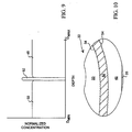
- a graph of ion concentration verses depth is shown after an anneal step for implanted phosphorous P 1 and P 2 as well as implanted nitrogen N. Concentration of nitrogen remains higher than concentration of phosphorous ions P 1 and P 2 . The peak densities are reduced and extended substantially across the respective conductive and insulative regions. Phosphorous ions P 1 form the lower conductive plate 48, phosphorous P 2 form the upper conductive plate 50, and nitrogen combined with silicon, forms the intermediate insulative material 52. At the juncture between conductive plate 48 and insulative material 52 is a slight decrease in phosphorous concentration. Likewise, at the interface between conductive plate 50 and insulative material 52, a slight decrease in phosphorous concentration is shown. Phosphorous ions P 1 can be used to form a source/drain n + region.
- Fig. 10 Part of the reason for the decrease in phosphorous concentration is due to cross-diffusion of nitrogen and phosphorous at the juncture. As shown in Fig. 10, diffusion across the juncture causes a textured demarcation between each region. The textured junction provides enhancement in the surface between the insulative and conductive regions. An increase in area, as shown by the textured juncture 54 causes a corresponding direct increase in capacitance.
- the detailed drawing of Fig. 10 is illustrative of a small portion of polysilicon 22, taken from Fig. 8. The remaining portions of polysilicon 22 demonstrate similar texturization between insulative region 52 and conductive regions 48 and 50.
- the present methodology can avoid contamination caused by deposition and thereby minimize any pinholes in the insulative region which would deleteriously affect capacitor operation. More importantly, the entire capacitor configuration can be formed from a single polysilicon layer which is preferably quite thin, e.g., approximately 1,000 Angstroms.
Landscapes
- Engineering & Computer Science (AREA)
- Manufacturing & Machinery (AREA)
- Semiconductor Integrated Circuits (AREA)
- Semiconductor Memories (AREA)
Applications Claiming Priority (2)
| Application Number | Priority Date | Filing Date | Title |
|---|---|---|---|
| US08/239,453 US5429972A (en) | 1994-05-09 | 1994-05-09 | Method of fabricating a capacitor with a textured polysilicon interface and an enhanced dielectric |
| US239453 | 1994-05-09 |
Publications (2)
| Publication Number | Publication Date |
|---|---|
| EP0682360A2 true EP0682360A2 (de) | 1995-11-15 |
| EP0682360A3 EP0682360A3 (de) | 1998-05-20 |
Family
ID=22902195
Family Applications (1)
| Application Number | Title | Priority Date | Filing Date |
|---|---|---|---|
| EP95302951A Withdrawn EP0682360A3 (de) | 1994-05-09 | 1995-05-01 | Verfahren zur Herstellung eines Kondensators aus einer Polysiliziumschicht |
Country Status (3)
| Country | Link |
|---|---|
| US (1) | US5429972A (de) |
| EP (1) | EP0682360A3 (de) |
| JP (1) | JPH0851189A (de) |
Families Citing this family (36)
| Publication number | Priority date | Publication date | Assignee | Title |
|---|---|---|---|---|
| US6001712A (en) * | 1993-03-16 | 1999-12-14 | Semiconductor Energy Laboratory Co., Ltd. | Insulated gate field effect semiconductor device and forming method thereof |
| US6507072B2 (en) | 1993-03-16 | 2003-01-14 | Semiconductor Energy Laboratory Co., Ltd. | Insulated gate field effect semiconductor device and forming method thereof |
| US5793076A (en) * | 1995-09-21 | 1998-08-11 | Micron Technology, Inc. | Scalable high dielectric constant capacitor |
| US5801104A (en) * | 1995-10-24 | 1998-09-01 | Micron Technology, Inc. | Uniform dielectric film deposition on textured surfaces |
| US5783470A (en) * | 1995-12-14 | 1998-07-21 | Lsi Logic Corporation | Method of making CMOS dynamic random-access memory structures and the like |
| KR0171098B1 (ko) * | 1995-12-19 | 1999-02-01 | 문정환 | 캐패시터 제조방법 |
| JP3125915B2 (ja) * | 1996-01-09 | 2001-01-22 | 日本電気株式会社 | 半導体装置の製造方法 |
| US5754390A (en) * | 1996-01-23 | 1998-05-19 | Micron Technology, Inc. | Integrated capacitor bottom electrode for use with conformal dielectric |
| JPH09307076A (ja) * | 1996-05-16 | 1997-11-28 | Nec Corp | 半導体装置の製造方法 |
| US5872049A (en) * | 1996-06-19 | 1999-02-16 | Advanced Micro Devices, Inc. | Nitrogenated gate structure for improved transistor performance and method for making same |
| US5882993A (en) | 1996-08-19 | 1999-03-16 | Advanced Micro Devices, Inc. | Integrated circuit with differing gate oxide thickness and process for making same |
| US5888295A (en) * | 1996-08-20 | 1999-03-30 | Micron Technology, Inc. | Method of forming a silicon film |
| US6528436B1 (en) | 1996-10-21 | 2003-03-04 | Micron Technology. Inc. | Method of forming silicon nitride layer directly on HSG polysilicon |
| US5770500A (en) * | 1996-11-15 | 1998-06-23 | Micron Technology, Inc. | Process for improving roughness of conductive layer |
| US5739064A (en) * | 1996-11-27 | 1998-04-14 | Micron Technology, Inc. | Second implanted matrix for agglomeration control and thermal stability |
| US6037639A (en) * | 1997-06-09 | 2000-03-14 | Micron Technology, Inc. | Fabrication of integrated devices using nitrogen implantation |
| US6249019B1 (en) | 1997-06-27 | 2001-06-19 | Micron Technology, Inc. | Container capacitor with increased surface area and method for making same |
| US5917213A (en) | 1997-08-21 | 1999-06-29 | Micron Technology, Inc. | Depletion compensated polysilicon electrodes |
| TW380295B (en) * | 1997-10-18 | 2000-01-21 | United Microelectronics Corp | Manufacturing method for DRAM capacitor dielectric |
| TW357430B (en) * | 1997-12-22 | 1999-05-01 | United Microelectronics Corp | Manufacturing method of capacitors |
| KR19990060472A (ko) * | 1997-12-31 | 1999-07-26 | 구본준 | 반도체소자의 산화막 형성방법 |
| US6268296B1 (en) * | 1997-12-31 | 2001-07-31 | Texas Instruments Incorporated | Low temperature process for multiple voltage devices |
| KR100258882B1 (ko) * | 1998-02-27 | 2000-06-15 | 김영환 | 반도체 소자의 제조 방법 |
| US6066525A (en) * | 1998-04-07 | 2000-05-23 | Lsi Logic Corporation | Method of forming DRAM capacitor by forming separate dielectric layers in a CMOS process |
| US6531364B1 (en) | 1998-08-05 | 2003-03-11 | Advanced Micro Devices, Inc. | Advanced fabrication technique to form ultra thin gate dielectric using a sacrificial polysilicon seed layer |
| US6177696B1 (en) | 1998-08-13 | 2001-01-23 | International Business Machines Corporation | Integration scheme enhancing deep trench capacitance in semiconductor integrated circuit devices |
| US6124164A (en) * | 1998-09-17 | 2000-09-26 | Micron Technology, Inc. | Method of making integrated capacitor incorporating high K dielectric |
| US6373114B1 (en) | 1998-10-23 | 2002-04-16 | Micron Technology, Inc. | Barrier in gate stack for improved gate dielectric integrity |
| US6238998B1 (en) | 1998-11-20 | 2001-05-29 | International Business Machines Corporation | Shallow trench isolation on a silicon substrate using nitrogen implant into the side wall |
| US6159874A (en) * | 1999-10-27 | 2000-12-12 | Infineon Technologies North America Corp. | Method of forming a hemispherical grained capacitor |
| US6458714B1 (en) | 2000-11-22 | 2002-10-01 | Micron Technology, Inc. | Method of selective oxidation in semiconductor manufacture |
| US6819540B2 (en) * | 2001-11-26 | 2004-11-16 | Shipley Company, L.L.C. | Dielectric structure |
| US6967384B2 (en) * | 2003-12-12 | 2005-11-22 | International Business Machines Corporation | Structure and method for ultra-small grain size polysilicon |
| US7384853B2 (en) * | 2005-08-25 | 2008-06-10 | United Microelectronics Corp. | Method of performing salicide processes on MOS transistors |
| US7977172B2 (en) * | 2008-12-08 | 2011-07-12 | Advanced Micro Devices, Inc. | Dynamic random access memory (DRAM) cells and methods for fabricating the same |
| US8642440B2 (en) | 2011-10-24 | 2014-02-04 | International Business Machines Corporation | Capacitor with deep trench ion implantation |
Family Cites Families (10)
| Publication number | Priority date | Publication date | Assignee | Title |
|---|---|---|---|---|
| JPS6258673A (ja) * | 1985-09-09 | 1987-03-14 | Fujitsu Ltd | 半導体記憶装置 |
| US4682407A (en) * | 1986-01-21 | 1987-07-28 | Motorola, Inc. | Means and method for stabilizing polycrystalline semiconductor layers |
| US4774197A (en) * | 1986-06-17 | 1988-09-27 | Advanced Micro Devices, Inc. | Method of improving silicon dioxide |
| US5043780A (en) * | 1990-01-03 | 1991-08-27 | Micron Technology, Inc. | DRAM cell having a texturized polysilicon lower capacitor plate for increased capacitance |
| US5208176A (en) * | 1990-01-16 | 1993-05-04 | Micron Technology, Inc. | Method of fabricating an enhanced dynamic random access memory (DRAM) cell capacitor using multiple polysilicon texturization |
| US5082797A (en) * | 1991-01-22 | 1992-01-21 | Micron Technology, Inc. | Method of making stacked textured container capacitor |
| US5102832A (en) * | 1991-02-11 | 1992-04-07 | Micron Technology, Inc. | Methods for texturizing polysilicon |
| US5138411A (en) * | 1991-05-06 | 1992-08-11 | Micron Technology, Inc. | Anodized polysilicon layer lower capacitor plate of a dram to increase capacitance |
| US5250456A (en) * | 1991-09-13 | 1993-10-05 | Sgs-Thomson Microelectronics, Inc. | Method of forming an integrated circuit capacitor dielectric and a capacitor formed thereby |
| US5191509A (en) * | 1991-12-11 | 1993-03-02 | International Business Machines Corporation | Textured polysilicon stacked trench capacitor |
-
1994
- 1994-05-09 US US08/239,453 patent/US5429972A/en not_active Expired - Fee Related
-
1995
- 1995-05-01 EP EP95302951A patent/EP0682360A3/de not_active Withdrawn
- 1995-05-08 JP JP7109464A patent/JPH0851189A/ja not_active Withdrawn
Also Published As
| Publication number | Publication date |
|---|---|
| US5429972A (en) | 1995-07-04 |
| EP0682360A3 (de) | 1998-05-20 |
| JPH0851189A (ja) | 1996-02-20 |
Similar Documents
| Publication | Publication Date | Title |
|---|---|---|
| US5429972A (en) | Method of fabricating a capacitor with a textured polysilicon interface and an enhanced dielectric | |
| US6331468B1 (en) | Formation of integrated circuit structure using one or more silicon layers for implantation and out-diffusion in formation of defect-free source/drain regions and also for subsequent formation of silicon nitride spacers | |
| US4269636A (en) | Method of fabricating self-aligned bipolar transistor process and device utilizing etching and self-aligned masking | |
| US6015739A (en) | Method of making gate dielectric for sub-half micron MOS transistors including a graded dielectric constant | |
| US4575920A (en) | Method of manufacturing an insulated-gate field-effect transistor | |
| KR100642627B1 (ko) | 다결정 실리콘 구조물의 제조 방법 | |
| US7084034B2 (en) | High voltage MOS-gated power device and related manufacturing process | |
| EP0859402A2 (de) | Verfahren zur Herstellung einer MOS Elektrode | |
| WO1996032738A1 (en) | A METHOD FOR INTRODUCTION OF AN IMPURITY DOPANT IN SiC, A SEMICONDUCTOR DEVICE FORMED BY THE METHOD AND A USE OF A HIGHLY DOPED AMORPHOUS LAYER AS A SOURCE FOR DOPANT DIFFUSION INTO SiC | |
| EP0852394B1 (de) | Verfahren zum Herstellen von flachen Übergängen in Siliziumbauelementen | |
| CA1204370A (en) | Method of forming a shallow and high conductivity boron doped layer in silicon | |
| EP0508679A1 (de) | Verfahren zur Herstellung einer Silizidschicht durch Ionenimplantation und so hergestelltes Halbleiterelement | |
| US5683920A (en) | Method for fabricating semiconductor devices | |
| US5599734A (en) | Method for fabricating MOS transistor utilizing doped disposable layer | |
| GB2314676A (en) | Method for forming shallow junction of a semiconductor device | |
| EP0110103B1 (de) | Verfahren zum Herstellen einer CMOS-Struktur | |
| JP3464247B2 (ja) | 半導体装置の製造方法 | |
| US5712196A (en) | Method for producing a low resistivity polycide | |
| US5468677A (en) | Isolation structure of semiconductor device and method for forming the same | |
| JP2624709B2 (ja) | 半導体装置の製造方法 | |
| US5973381A (en) | MOS capacitor and MOS capacitor fabrication method | |
| US7118977B2 (en) | System and method for improved dopant profiles in CMOS transistors | |
| US7700431B2 (en) | Method for manufacturing a semiconductor device having polysilicon plugs | |
| RU1830156C (ru) | Способ изготовлени полупроводниковых приборов | |
| CN1072390C (zh) | 在半导体基底上进行离子注入的方法 |
Legal Events
| Date | Code | Title | Description |
|---|---|---|---|
| PUAI | Public reference made under article 153(3) epc to a published international application that has entered the european phase |
Free format text: ORIGINAL CODE: 0009012 |
|
| AK | Designated contracting states |
Kind code of ref document: A2 Designated state(s): AT BE DE DK ES FR GB GR IE IT LU NL PT SE |
|
| PUAL | Search report despatched |
Free format text: ORIGINAL CODE: 0009013 |
|
| AK | Designated contracting states |
Kind code of ref document: A3 Designated state(s): AT BE DE DK ES FR GB GR IE IT LU NL PT SE |
|
| 17P | Request for examination filed |
Effective date: 19981026 |
|
| 17Q | First examination report despatched |
Effective date: 19991111 |
|
| STAA | Information on the status of an ep patent application or granted ep patent |
Free format text: STATUS: THE APPLICATION IS DEEMED TO BE WITHDRAWN |
|
| 18D | Application deemed to be withdrawn |
Effective date: 20031202 |