EP0682367A1 - Dispositif semi-conducteur encapsulé et son procédé de fabrication - Google Patents
Dispositif semi-conducteur encapsulé et son procédé de fabrication Download PDFInfo
- Publication number
- EP0682367A1 EP0682367A1 EP95109303A EP95109303A EP0682367A1 EP 0682367 A1 EP0682367 A1 EP 0682367A1 EP 95109303 A EP95109303 A EP 95109303A EP 95109303 A EP95109303 A EP 95109303A EP 0682367 A1 EP0682367 A1 EP 0682367A1
- Authority
- EP
- European Patent Office
- Prior art keywords
- jig
- interconnection member
- resin package
- package body
- interconnection
- Prior art date
- Legal status (The legal status is an assumption and is not a legal conclusion. Google has not performed a legal analysis and makes no representation as to the accuracy of the status listed.)
- Granted
Links
Images


Classifications
-
- H—ELECTRICITY
- H10—SEMICONDUCTOR DEVICES; ELECTRIC SOLID-STATE DEVICES NOT OTHERWISE PROVIDED FOR
- H10P—GENERIC PROCESSES OR APPARATUS FOR THE MANUFACTURE OR TREATMENT OF DEVICES COVERED BY CLASS H10
- H10P72/00—Handling or holding of wafers, substrates or devices during manufacture or treatment thereof
- H10P72/04—Apparatus for manufacture or treatment
- H10P72/0441—Apparatus for sealing, encapsulating, glassing, decapsulating or the like
-
- H—ELECTRICITY
- H05—ELECTRIC TECHNIQUES NOT OTHERWISE PROVIDED FOR
- H05K—PRINTED CIRCUITS; CASINGS OR CONSTRUCTIONAL DETAILS OF ELECTRIC APPARATUS; MANUFACTURE OF ASSEMBLAGES OF ELECTRICAL COMPONENTS
- H05K3/00—Apparatus or processes for manufacturing printed circuits
- H05K3/30—Assembling printed circuits with electric components, e.g. with resistors
- H05K3/32—Assembling printed circuits with electric components, e.g. with resistors electrically connecting electric components or wires to printed circuits
- H05K3/34—Assembling printed circuits with electric components, e.g. with resistors electrically connecting electric components or wires to printed circuits by soldering
- H05K3/3465—Application of solder
- H05K3/3478—Application of solder preforms; Transferring prefabricated solder patterns
-
- H—ELECTRICITY
- H10—SEMICONDUCTOR DEVICES; ELECTRIC SOLID-STATE DEVICES NOT OTHERWISE PROVIDED FOR
- H10W—GENERIC PACKAGES, INTERCONNECTIONS, CONNECTORS OR OTHER CONSTRUCTIONAL DETAILS OF DEVICES COVERED BY CLASS H10
- H10W70/00—Package substrates; Interposers; Redistribution layers [RDL]
- H10W70/01—Manufacture or treatment
- H10W70/04—Manufacture or treatment of leadframes
- H10W70/041—Connecting or disconnecting interconnections to or from leadframes, e.g. connecting bond wires or bumps
-
- H—ELECTRICITY
- H10—SEMICONDUCTOR DEVICES; ELECTRIC SOLID-STATE DEVICES NOT OTHERWISE PROVIDED FOR
- H10W—GENERIC PACKAGES, INTERCONNECTIONS, CONNECTORS OR OTHER CONSTRUCTIONAL DETAILS OF DEVICES COVERED BY CLASS H10
- H10W70/00—Package substrates; Interposers; Redistribution layers [RDL]
- H10W70/40—Leadframes
- H10W70/464—Additional interconnections in combination with leadframes
-
- H—ELECTRICITY
- H10—SEMICONDUCTOR DEVICES; ELECTRIC SOLID-STATE DEVICES NOT OTHERWISE PROVIDED FOR
- H10W—GENERIC PACKAGES, INTERCONNECTIONS, CONNECTORS OR OTHER CONSTRUCTIONAL DETAILS OF DEVICES COVERED BY CLASS H10
- H10W74/00—Encapsulations, e.g. protective coatings
- H10W74/01—Manufacture or treatment
- H10W74/016—Manufacture or treatment using moulds
-
- H—ELECTRICITY
- H05—ELECTRIC TECHNIQUES NOT OTHERWISE PROVIDED FOR
- H05K—PRINTED CIRCUITS; CASINGS OR CONSTRUCTIONAL DETAILS OF ELECTRIC APPARATUS; MANUFACTURE OF ASSEMBLAGES OF ELECTRICAL COMPONENTS
- H05K2203/00—Indexing scheme relating to apparatus or processes for manufacturing printed circuits covered by H05K3/00
- H05K2203/01—Tools for processing; Objects used during processing
- H05K2203/0104—Tools for processing; Objects used during processing for patterning or coating
- H05K2203/0113—Female die used for patterning or transferring, e.g. temporary substrate having recessed pattern
-
- H—ELECTRICITY
- H05—ELECTRIC TECHNIQUES NOT OTHERWISE PROVIDED FOR
- H05K—PRINTED CIRCUITS; CASINGS OR CONSTRUCTIONAL DETAILS OF ELECTRIC APPARATUS; MANUFACTURE OF ASSEMBLAGES OF ELECTRICAL COMPONENTS
- H05K2203/00—Indexing scheme relating to apparatus or processes for manufacturing printed circuits covered by H05K3/00
- H05K2203/03—Metal processing
- H05K2203/0338—Transferring metal or conductive material other than a circuit pattern, e.g. bump, solder, printed component
-
- H—ELECTRICITY
- H05—ELECTRIC TECHNIQUES NOT OTHERWISE PROVIDED FOR
- H05K—PRINTED CIRCUITS; CASINGS OR CONSTRUCTIONAL DETAILS OF ELECTRIC APPARATUS; MANUFACTURE OF ASSEMBLAGES OF ELECTRICAL COMPONENTS
- H05K2203/00—Indexing scheme relating to apparatus or processes for manufacturing printed circuits covered by H05K3/00
- H05K2203/04—Soldering or other types of metallurgic bonding
- H05K2203/041—Solder preforms in the shape of solder balls
-
- H—ELECTRICITY
- H05—ELECTRIC TECHNIQUES NOT OTHERWISE PROVIDED FOR
- H05K—PRINTED CIRCUITS; CASINGS OR CONSTRUCTIONAL DETAILS OF ELECTRIC APPARATUS; MANUFACTURE OF ASSEMBLAGES OF ELECTRICAL COMPONENTS
- H05K2203/00—Indexing scheme relating to apparatus or processes for manufacturing printed circuits covered by H05K3/00
- H05K2203/08—Treatments involving gases
- H05K2203/082—Suction, e.g. for holding solder balls or components
-
- H—ELECTRICITY
- H10—SEMICONDUCTOR DEVICES; ELECTRIC SOLID-STATE DEVICES NOT OTHERWISE PROVIDED FOR
- H10W—GENERIC PACKAGES, INTERCONNECTIONS, CONNECTORS OR OTHER CONSTRUCTIONAL DETAILS OF DEVICES COVERED BY CLASS H10
- H10W74/00—Encapsulations, e.g. protective coatings
-
- H—ELECTRICITY
- H10—SEMICONDUCTOR DEVICES; ELECTRIC SOLID-STATE DEVICES NOT OTHERWISE PROVIDED FOR
- H10W—GENERIC PACKAGES, INTERCONNECTIONS, CONNECTORS OR OTHER CONSTRUCTIONAL DETAILS OF DEVICES COVERED BY CLASS H10
- H10W90/00—Package configurations
- H10W90/701—Package configurations characterised by the relative positions of pads or connectors relative to package parts
- H10W90/751—Package configurations characterised by the relative positions of pads or connectors relative to package parts of bond wires
- H10W90/754—Package configurations characterised by the relative positions of pads or connectors relative to package parts of bond wires between a chip and a stacked insulating package substrate, interposer or RDL
Definitions
- the present invention generally relates to packaging of semiconductor devices, and more particularly to a packaged semiconductor device that can be produced with a reduced cost.
- the integration density of integrated circuits formed on a semiconductor chip is increasing ever and ever.
- the packages used for accommodating the semiconductor chip is also required to have a capability of providing a large number of interconnections leads in correspondence to the increased number of terminals on the chip.
- FIG.1 shows a conventional package 10 of the so-called QFP (quad flat package) type wherein a number of leads 11 are provided along the side of a package body 12.
- the leads 11 project laterally in the outward direction from the package body 12 and bent downward. Further, the leads 11 are bent again in the horizontal direction and form the terminals 11a that extend laterally from the body 12. Thereby, a so-called gull-wing type terminal is formed.
- this type of package having the leads along the side wall of the package body, has a problem of insufficient location for providing the interconnection leads and is not suitable for accommodating semiconductor devices having a large integration density. Further, this type of package tends to show a variation in the vertical level of the terminal part 11a of the lead 11. Generally, the level of the terminal 11a may change as much as 100 ⁇ m. However, such a large variation in the level of the terminal is not desirable from the view point of reliable interconnection.
- a so-called PGA (pin grid array) package is proposed as shown in FIG.2, wherein a large number of interconnection pins 21 are arranged in rows and columns on the bottom surface of a package body 22.
- This PGA package has a problem in that a process for embedding the pins 21 on the package body 22 is necessary.
- this process includes processes of introducing a large number of minute metal rods on a package body, and apply shaking until the metal rods are settled in the holes formed in the package body as the pins 21. After the pins are settled, it is necessary to fix the pins on the package body 22.
- the process for fabricating the PGA package is time consuming and increases the cost of the device.
- Another object of the present invention is to provide a packaged semiconductor device and a manufacturing method therefore, wherein the cost for manufacturing the device is reduced.
- Another object of the present invention is to provide a semiconductor device having a package and a manufacturing method thereof, wherein metal spheres are arranged in a row and column formation on a bottom surface of a package body as interconnection leads.
- arrangement of the spheres in the row and column formation is achieved easily by using a jig that has a number of depressions arranged in correspondence to the row and column pattern of the interconnection leads. By applying a suction through the depressions, one can hold the spheres on the jig stably, and the spheres are connected mechanically as well as electrically to a lead frame either by welding or other processes such as passing through an annealing furnace.
- the spheres in the desired pattern such as the row and column formation, and the cost for manufacturing the device is decreased significantly. Further, by forming the depressions with a uniform diameter, one can set the amount of projection of the spheres from the bottom surface of the package body at exactly the same level. Thereby, a reliable electric interconnection to the external apparatuses can be achieved when the semiconductor device is mounted on a printed circuit board and the like.
- FIGS.3(A) and 3(B) show a semiconductor device 31 according to a first embodiment of the present invention.
- a semiconductor chip 35 (not shown in these drawings, see FIGS.4(A) - 4(C)) is accommodated in a plastic package body 32, and a number of interconnection leads 33 are provided on the bottom surface of the package body 32 similar to the device of the PGA type.
- the interconnection leads are formed from a number of metal spheres arranged in the row and column formation, and projects downward from the bottom surface of the package body 32 by a distance of about 30 ⁇ m or less.
- the magnitude of projection d is extremely uniform throughout the spheres. The deviation is less than 5 ⁇ m, usually less than 1 ⁇ m.
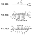
- FIGS.4(A) - 4(F) show the process for manufacturing the device of FIGS.3(A) and 3(B) according to the first embodiment.
- the semiconductor chip 35 mentioned previously is mounted on a lead frame 34. Further, the bonding pads formed on the semiconductor chip 35 are connected to an inner lead 34a of the lead frame 34 by a bonding wire as usual.
- the metal spheres 33 each having a same diameter of 1mm, for example, are supplied to a jig 36.
- a number of depressions 39 are formed in a row and column formation in correspondence to the row and column formation of the spheres 33 on the bottom surface of the package body 32 shown in FIG.3(B).
- a hole 10 is formed to penetrate through the body of the jig 36.
- the jig 36 is turned over as shown in FIG.4(C) and the spheres 33 that have failed settling in the depressions 39 fall off from the jig 36.
- the foregoing lead frame 34 is placed on the jig 36 as shown in FIG.4(D).
- the jig 36 is formed with a support member 38a that extends to surround the region where the depressions 33 is formed, and the lead frame 34 thus placed is held by the support member 38a.
- guide pins 37a and 37b are formed on the jig 36, and the guide pins engage with corresponding openings formed on the lead frame 34 when the lead frame 34 is properly positioned.
- the uppermost part of the spheres 33 is aligned on a flat plane and is contacted to the flat lower major surface of the lead frame 34 with precision.
- these metal spheres can be manufactured with high precision.
- the JIS Japanese Industrial Standard
- the allowance of diameter of metal spheres be less than 5 ⁇ m.
- the lead frame 34 is held stably on the jig 36 by the air pressure that is caused by the vacuum suction applied to the rear side of the jig 36.
- the penetrating hole 40 is provided also in correspondence to the support member 38a.
- a laser beam 12 is irradiated onto the lead frame 34 in correspondence to where the spheres 33 are located underneath.
- a part 34a of the lead frame 34 is caused to melt to form a fused region 34a that fuses with the metal sphere 33 as shown in FIG.4(E).
- a laser welding of the spheres 33 and the lead frame 34 is established.
- the lead frame 34 is removed from the jig 36 together with the semiconductor chip 35 as well as the metal spheres 33 that are welded to the lead frame 34, and the lead frame 34 is placed on a second jig 43 as shown in FIG.4(F).
- the jig 43 includes an upper mold 43a and a lower mold 43b, wherein the upper and lower molds are formed with spaces 43c and 43d corresponding to the resin package body 32 of the device of FIG.3(A).
- a number of depressions 45 are formed in the row and column formation in correspondence to the row and column formation of the metal spheres on the lead frame 34. Further, each depression 45 is evacuated via a hole 47 penetrating through the lower mold 43b.
- guide pins 44a and 44b are provided on the lower mold 43b, and corresponding depressions are provided in the upper mold 43a.
- the pins 44a and 44b may be provided to engage with the openings formed in the lead frame 34 for accommodating the guide pins 37a and 37b of the jig 36.
- FIG.5 shows the process for achieving a uniform projection d of the spherical leads 33 in the semiconductor device 31.
- the depression 45 has a diameter x that is set smaller than the diameter of the spheres 33.
- a space 48 is formed between the sphere 33 and the mold 43b, and this space 48 is evacuated via the penetrating hole 47.
- the metal spheres can be manufactured to have a highly uniform diameter with the tolerance of less than 5 ⁇ m, typically less than 1 ⁇ m, one can determine the vertical positioning level of the spheres 33 on the mold 43b by setting the diameter x of the circular opening formed at the surface of the mold 43b in correspondence to the semi-spherical depression 45.
- the variation of the projection d can be set smaller than a few microns.
- the space 48 of course produces a negative pressure when evacuated via the hole 47 and the lead frame 34 is firmly held on the mold 43b.
- the diameter of the spheres is set to 0.5 - 2mm.
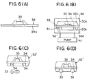
- the semiconductor chip 35 is mounted on the lead frame 34 and electric connection between the chip 35 and the inner lead 34a is established similarly to the first embodiment.
- the lead frame 34 is incorporated into a jig 50 that includes an upper mold 50a and a lower mold 50b.
- the upper mold 50a is formed with a space 50c corresponding to the package body 32 of FIG.3(A).
- the lower mold 50b is formed with a space 50d corresponding to the package body 32 of FIG.3(B).
- the lower mold 50b there are formed a number of projections 51 in correspondence to the space 50d, such that the projections 51 support the lead frame 34 when the lead frame 34 is mounted on the mold 50b.
- a hole 52 is formed and the lead frame 34 is held firmly on the projections 51 when a vacuum is applied by the pump 41.
- the projections 51 are arranged in a row and column formation in correspondence to the row and column arrangement of the spherical leads 33 on the bottom surface of the package body 32 shown in FIG.3(B).
- the region of the lead frame 34 that is supported by the projections 51 is not covered by the plastic.
- a packaged body 32' having a number of holes 54 at the bottom surface is obtained upon the curing of the plastic. See FIG.6(C).
- the holes 54 are arranged in the row and column formation, and the lead frame 34 is exposed through these holes 54.
- the package body 32' is turned over and the metal spheres 33 are poured on the bottom surface now facing upward.
- the package body 32' is passed through an annealing process.
- a metal having a low melting point such as solder is used for the sphere 33.
- the surface of the sphere 33 is coated by such a metal.
- the spheres 33 cause melting upon annealing and establishes a mechanical as well as electric connection to the lead frame 34. See FIG.6(D).
- the step for using the jig is reduced and the efficiency of production is improved further.
- the present embodiment can be applicable to the QFP type package.
- the projections 51 of the jig 50 are arranged along the lateral edge of the package body 32' to be formed, in conformity with the leads that extends laterally from the package body 32'.
- grooves extending laterally are formed in the bottom surface of the package body 32' instead of the holes 54.
- the vertical level of the pins 33a is aligned exactly on a horizontal plane S, and the problem of the variation in the level of the leads pertinent to the conventional QFP type devices that use the gull-wing type leads, is successfully eliminated.
- FIG.8 shows another embodiment wherein the present invention is applied to the TAB (Tape Automated Bonding) process.
- the semiconductor chip 35 is mounted on a tape carrier 60 on which a conductor pattern 31 is formed.
- the spherical lead 33 is connected to this conductor pattern 31 on the carrier 60.
- a jig similar to the jig 36 of the first embodiment is used. As the process is readily derived from the previous description, further description of the present invention will be omitted.
- FIG.9 shows still other embodiment of the present invention, wherein the present invention is applied to the COB (Chip on Board) process.
- COB Chip on Board
- the semiconductor chip 35 is mounted on a board or substrate 62 that carries conductor patterns 63 and 64 respectively on the upper and lower major surfaces of the substrate 62.
- the upper conductor pattern 63 is connected to the lower conductor pattern 64 via a through hole formed in the substrate 62.
- the spherical leads 33 are mounted on the lower conductor pattern 63 as illustrated. In this case, too, the spheres 33 are held on the depressions formed in a jig similar to the jig 36.
- another jig similar to the jig 43 may be used.
- the leads used in the present invention is not limited to the spherical leads as described with reference to the first and second embodiments, but any lead may be used as long as it can easily roll on the jig when arranging the leads in a predetermined pattern.
- the arrangement of the lead is not limited to the row and column formation but any other pattern may be used.
- the connection of the leads to the lead frame may be made by various welding processes other than the laser beam welding. For example, an electric welding may be used in the process of FIG.4(E).
Landscapes
- Engineering & Computer Science (AREA)
- Manufacturing & Machinery (AREA)
- Microelectronics & Electronic Packaging (AREA)
- Lead Frames For Integrated Circuits (AREA)
- Encapsulation Of And Coatings For Semiconductor Or Solid State Devices (AREA)
Applications Claiming Priority (3)
| Application Number | Priority Date | Filing Date | Title |
|---|---|---|---|
| JP2165979A JPH0462865A (ja) | 1990-06-25 | 1990-06-25 | 半導体装置及びその製造方法 |
| JP165979/90 | 1990-06-25 | ||
| EP91110062A EP0463559B1 (fr) | 1990-06-25 | 1991-06-19 | Dispositif semi-conducteur encapsulé et son procédé de fabrication |
Related Parent Applications (1)
| Application Number | Title | Priority Date | Filing Date |
|---|---|---|---|
| EP91110062.6 Division | 1991-06-19 |
Publications (2)
| Publication Number | Publication Date |
|---|---|
| EP0682367A1 true EP0682367A1 (fr) | 1995-11-15 |
| EP0682367B1 EP0682367B1 (fr) | 1997-09-03 |
Family
ID=15822631
Family Applications (2)
| Application Number | Title | Priority Date | Filing Date |
|---|---|---|---|
| EP95109303A Expired - Lifetime EP0682367B1 (fr) | 1990-06-25 | 1991-06-19 | Dispositif semi-conducteur encapsulé et son procédé de fabrication |
| EP91110062A Expired - Lifetime EP0463559B1 (fr) | 1990-06-25 | 1991-06-19 | Dispositif semi-conducteur encapsulé et son procédé de fabrication |
Family Applications After (1)
| Application Number | Title | Priority Date | Filing Date |
|---|---|---|---|
| EP91110062A Expired - Lifetime EP0463559B1 (fr) | 1990-06-25 | 1991-06-19 | Dispositif semi-conducteur encapsulé et son procédé de fabrication |
Country Status (4)
| Country | Link |
|---|---|
| EP (2) | EP0682367B1 (fr) |
| JP (1) | JPH0462865A (fr) |
| KR (1) | KR960000599B1 (fr) |
| DE (2) | DE69125657T2 (fr) |
Cited By (2)
| Publication number | Priority date | Publication date | Assignee | Title |
|---|---|---|---|---|
| EP0874400A1 (fr) * | 1997-04-21 | 1998-10-28 | Oki Electric Industry Co., Ltd. | Dispositif semi-conducteur |
| EP0780896A3 (fr) * | 1995-12-19 | 1999-04-14 | Texas Instruments Incorporated | Boítier électronique amélioré |
Families Citing this family (3)
| Publication number | Priority date | Publication date | Assignee | Title |
|---|---|---|---|---|
| JP2531382B2 (ja) * | 1994-05-26 | 1996-09-04 | 日本電気株式会社 | ボ―ルグリッドアレイ半導体装置およびその製造方法 |
| FR2722915B1 (fr) * | 1994-07-21 | 1997-01-24 | Sgs Thomson Microelectronics | Boitier bga a moulage par injection |
| KR101479511B1 (ko) | 2008-05-26 | 2015-01-07 | 삼성전자주식회사 | 반도체 패키지 및 그 제조 방법 |
Citations (3)
| Publication number | Priority date | Publication date | Assignee | Title |
|---|---|---|---|---|
| US3959874A (en) * | 1974-12-20 | 1976-06-01 | Western Electric Company, Inc. | Method of forming an integrated circuit assembly |
| JPS62266857A (ja) * | 1986-05-15 | 1987-11-19 | Oki Electric Ind Co Ltd | 半導体装置 |
| WO1988006395A1 (fr) * | 1987-02-19 | 1988-08-25 | Olin Corporation | Procede de production de grilles de fiches en plastique et grilles ainsi produites |
Family Cites Families (4)
| Publication number | Priority date | Publication date | Assignee | Title |
|---|---|---|---|---|
| DE3173078D1 (en) * | 1981-12-29 | 1986-01-09 | Ibm | Soldering method of pins to eyelets of conductors formed on a ceramic substrate |
| JPS6049655A (ja) * | 1983-08-26 | 1985-03-18 | Fujitsu Ltd | リ−ドレスチップキャリアのバンプ形成方法 |
| JPS62142338A (ja) * | 1985-12-17 | 1987-06-25 | Shinko Electric Ind Co Ltd | 半導体装置用パツケ−ジ |
| EP0263222B1 (fr) * | 1986-10-08 | 1992-03-25 | International Business Machines Corporation | Procédé pour la formation de bornes de brasure pour un module en céramique sans broches |
-
1990
- 1990-06-25 JP JP2165979A patent/JPH0462865A/ja active Pending
-
1991
- 1991-06-19 EP EP95109303A patent/EP0682367B1/fr not_active Expired - Lifetime
- 1991-06-19 DE DE69125657T patent/DE69125657T2/de not_active Expired - Fee Related
- 1991-06-19 EP EP91110062A patent/EP0463559B1/fr not_active Expired - Lifetime
- 1991-06-19 DE DE69127559T patent/DE69127559T2/de not_active Expired - Fee Related
- 1991-06-25 KR KR1019910010572A patent/KR960000599B1/ko not_active Expired - Fee Related
Patent Citations (3)
| Publication number | Priority date | Publication date | Assignee | Title |
|---|---|---|---|---|
| US3959874A (en) * | 1974-12-20 | 1976-06-01 | Western Electric Company, Inc. | Method of forming an integrated circuit assembly |
| JPS62266857A (ja) * | 1986-05-15 | 1987-11-19 | Oki Electric Ind Co Ltd | 半導体装置 |
| WO1988006395A1 (fr) * | 1987-02-19 | 1988-08-25 | Olin Corporation | Procede de production de grilles de fiches en plastique et grilles ainsi produites |
Non-Patent Citations (3)
| Title |
|---|
| "Silicon Alignment Frame for Spherical Standoff Placement", IBM TECHNICAL DISCLOSURE BULLETIN, vol. 25, no. 5, NEW YORK US, pages 2590 * |
| J. LYMAN: "Solder Columns Secure Chip Carriers to Epoxy", ELECTRONICS DE 1984 A 1985 : ELECTRONICS WEEK., vol. 58, no. 37, NEW YORK US, pages 20 - 21, XP001450079 * |
| PATENT ABSTRACTS OF JAPAN vol. 12, no. 150 (E - 606) 10 May 1988 (1988-05-10) * |
Cited By (4)
| Publication number | Priority date | Publication date | Assignee | Title |
|---|---|---|---|---|
| EP0780896A3 (fr) * | 1995-12-19 | 1999-04-14 | Texas Instruments Incorporated | Boítier électronique amélioré |
| EP0874400A1 (fr) * | 1997-04-21 | 1998-10-28 | Oki Electric Industry Co., Ltd. | Dispositif semi-conducteur |
| US6084300A (en) * | 1997-04-21 | 2000-07-04 | Oki Electric Industry Co., Ltd. | Compact resin-sealed semiconductor device |
| KR100373569B1 (ko) * | 1997-04-21 | 2003-06-18 | 오끼 덴끼 고오교 가부시끼가이샤 | 반도체장치 |
Also Published As
| Publication number | Publication date |
|---|---|
| DE69125657T2 (de) | 1997-07-31 |
| KR960000599B1 (ko) | 1996-01-09 |
| EP0682367B1 (fr) | 1997-09-03 |
| EP0463559B1 (fr) | 1997-04-16 |
| EP0463559A3 (en) | 1992-03-25 |
| DE69127559T2 (de) | 1998-01-08 |
| EP0463559A2 (fr) | 1992-01-02 |
| DE69127559D1 (de) | 1997-10-09 |
| DE69125657D1 (de) | 1997-05-22 |
| JPH0462865A (ja) | 1992-02-27 |
Similar Documents
| Publication | Publication Date | Title |
|---|---|---|
| US5403776A (en) | Process of using a jig to align and mount terminal conductors to a semiconductor plastic package | |
| US3902148A (en) | Semiconductor lead structure and assembly and method for fabricating same | |
| US4026008A (en) | Semiconductor lead structure and assembly and method for fabricating same | |
| US5200366A (en) | Semiconductor device, its fabrication method and molding apparatus used therefor | |
| US5643835A (en) | Process for manufacturing and mounting a semiconductor device leadframe having alignment tabs | |
| JP3069792B2 (ja) | チップサイズ半導体パッケ―ジ及びその集合体並びにその製造方法 | |
| US6617193B1 (en) | Semiconductor device, semiconductor device substrate, and methods of fabricating the same | |
| JP2875139B2 (ja) | 半導体装置の製造方法 | |
| US5843798A (en) | Method for manufacturing semiconductor device having step of forming electrode pins on semiconductor chip using electrode-pin forming mask, and method for testing semiconductor chip using electrode-pin forming mask | |
| US6650020B2 (en) | Resin-sealed semiconductor device | |
| KR20030051222A (ko) | 반도체 장치 및 그 제조 방법 | |
| US5541447A (en) | Lead frame | |
| US20030218055A1 (en) | Integrated circuit packages without solder mask and method for the same | |
| EP0682367B1 (fr) | Dispositif semi-conducteur encapsulé et son procédé de fabrication | |
| US7546941B2 (en) | Ball attaching apparatus for correcting warpage of substrate and method of attaching solder balls using the same | |
| US6872650B2 (en) | Ball electrode forming method | |
| JP3288654B2 (ja) | 電気コネクタの製造方法 | |
| KR20010001159A (ko) | 비아 홀을 이용한 웨이퍼 레벨 칩 스케일 패키지 및 그 제조방법 | |
| JPH07226475A (ja) | 半導体装置及びその製造方法及びリードフレーム | |
| JPH08125062A (ja) | 半導体装置とその製造方法 | |
| JPH07302967A (ja) | 金属メッキによるバンプの形成方法 | |
| KR0182506B1 (ko) | 동시에 절단된 반도체 칩을 이용한 고밀도 실장형 패키지 및 그 제조 방법 | |
| US6551855B1 (en) | Substrate strip and manufacturing method thereof | |
| JPH11251726A (ja) | グリッドアレイ型半導体パッケージの実装方法 | |
| JPH08274205A (ja) | 半導体装置及びその製造方法 |
Legal Events
| Date | Code | Title | Description |
|---|---|---|---|
| PUAI | Public reference made under article 153(3) epc to a published international application that has entered the european phase |
Free format text: ORIGINAL CODE: 0009012 |
|
| 17P | Request for examination filed |
Effective date: 19950620 |
|
| AC | Divisional application: reference to earlier application |
Ref document number: 463559 Country of ref document: EP |
|
| AK | Designated contracting states |
Kind code of ref document: A1 Designated state(s): DE FR GB |
|
| GRAG | Despatch of communication of intention to grant |
Free format text: ORIGINAL CODE: EPIDOS AGRA |
|
| 17Q | First examination report despatched |
Effective date: 19960819 |
|
| GRAH | Despatch of communication of intention to grant a patent |
Free format text: ORIGINAL CODE: EPIDOS IGRA |
|
| GRAH | Despatch of communication of intention to grant a patent |
Free format text: ORIGINAL CODE: EPIDOS IGRA |
|
| GRAA | (expected) grant |
Free format text: ORIGINAL CODE: 0009210 |
|
| AC | Divisional application: reference to earlier application |
Ref document number: 463559 Country of ref document: EP |
|
| AK | Designated contracting states |
Kind code of ref document: B1 Designated state(s): DE FR GB |
|
| REF | Corresponds to: |
Ref document number: 69127559 Country of ref document: DE Date of ref document: 19971009 |
|
| ET | Fr: translation filed | ||
| PLBE | No opposition filed within time limit |
Free format text: ORIGINAL CODE: 0009261 |
|
| STAA | Information on the status of an ep patent application or granted ep patent |
Free format text: STATUS: NO OPPOSITION FILED WITHIN TIME LIMIT |
|
| 26N | No opposition filed | ||
| REG | Reference to a national code |
Ref country code: GB Ref legal event code: IF02 |
|
| PGFP | Annual fee paid to national office [announced via postgrant information from national office to epo] |
Ref country code: FR Payment date: 20020610 Year of fee payment: 12 |
|
| PGFP | Annual fee paid to national office [announced via postgrant information from national office to epo] |
Ref country code: GB Payment date: 20020619 Year of fee payment: 12 |
|
| PGFP | Annual fee paid to national office [announced via postgrant information from national office to epo] |
Ref country code: DE Payment date: 20020626 Year of fee payment: 12 |
|
| PG25 | Lapsed in a contracting state [announced via postgrant information from national office to epo] |
Ref country code: GB Free format text: LAPSE BECAUSE OF NON-PAYMENT OF DUE FEES Effective date: 20030619 |
|
| PG25 | Lapsed in a contracting state [announced via postgrant information from national office to epo] |
Ref country code: DE Free format text: LAPSE BECAUSE OF NON-PAYMENT OF DUE FEES Effective date: 20040101 |
|
| GBPC | Gb: european patent ceased through non-payment of renewal fee |
Effective date: 20030619 |
|
| PG25 | Lapsed in a contracting state [announced via postgrant information from national office to epo] |
Ref country code: FR Free format text: LAPSE BECAUSE OF NON-PAYMENT OF DUE FEES Effective date: 20040227 |
|
| REG | Reference to a national code |
Ref country code: FR Ref legal event code: ST |