EP0684633A2 - Méthode de fabrication d'un dispositif semi-conducteur - Google Patents
Méthode de fabrication d'un dispositif semi-conducteur Download PDFInfo
- Publication number
- EP0684633A2 EP0684633A2 EP95105463A EP95105463A EP0684633A2 EP 0684633 A2 EP0684633 A2 EP 0684633A2 EP 95105463 A EP95105463 A EP 95105463A EP 95105463 A EP95105463 A EP 95105463A EP 0684633 A2 EP0684633 A2 EP 0684633A2
- Authority
- EP
- European Patent Office
- Prior art keywords
- layer
- manufacturing
- semiconductor layer
- semiconductor
- temperature
- Prior art date
- Legal status (The legal status is an assumption and is not a legal conclusion. Google has not performed a legal analysis and makes no representation as to the accuracy of the status listed.)
- Withdrawn
Links
Images


Classifications
-
- H—ELECTRICITY
- H10—SEMICONDUCTOR DEVICES; ELECTRIC SOLID-STATE DEVICES NOT OTHERWISE PROVIDED FOR
- H10D—INORGANIC ELECTRIC SEMICONDUCTOR DEVICES
- H10D30/00—Field-effect transistors [FET]
- H10D30/01—Manufacture or treatment
- H10D30/061—Manufacture or treatment of FETs having Schottky gates
- H10D30/0612—Manufacture or treatment of FETs having Schottky gates of lateral single-gate Schottky FETs
- H10D30/0614—Manufacture or treatment of FETs having Schottky gates of lateral single-gate Schottky FETs using processes wherein the final gate is made after the completion of the source and drain regions, e.g. gate-last processes using dummy gates
-
- H—ELECTRICITY
- H10—SEMICONDUCTOR DEVICES; ELECTRIC SOLID-STATE DEVICES NOT OTHERWISE PROVIDED FOR
- H10D—INORGANIC ELECTRIC SEMICONDUCTOR DEVICES
- H10D30/00—Field-effect transistors [FET]
- H10D30/01—Manufacture or treatment
- H10D30/015—Manufacture or treatment of FETs having heterojunction interface channels or heterojunction gate electrodes, e.g. HEMT
-
- H—ELECTRICITY
- H10—SEMICONDUCTOR DEVICES; ELECTRIC SOLID-STATE DEVICES NOT OTHERWISE PROVIDED FOR
- H10D—INORGANIC ELECTRIC SEMICONDUCTOR DEVICES
- H10D30/00—Field-effect transistors [FET]
- H10D30/60—Insulated-gate field-effect transistors [IGFET]
- H10D30/67—Thin-film transistors [TFT]
- H10D30/6729—Thin-film transistors [TFT] characterised by the electrodes
- H10D30/6737—Thin-film transistors [TFT] characterised by the electrodes characterised by the electrode materials
- H10D30/6738—Schottky barrier electrodes
-
- H—ELECTRICITY
- H10—SEMICONDUCTOR DEVICES; ELECTRIC SOLID-STATE DEVICES NOT OTHERWISE PROVIDED FOR
- H10D—INORGANIC ELECTRIC SEMICONDUCTOR DEVICES
- H10D30/00—Field-effect transistors [FET]
- H10D30/60—Insulated-gate field-effect transistors [IGFET]
- H10D30/67—Thin-film transistors [TFT]
- H10D30/674—Thin-film transistors [TFT] characterised by the active materials
- H10D30/675—Group III-V materials, Group II-VI materials, Group IV-VI materials, selenium or tellurium
-
- H—ELECTRICITY
- H10—SEMICONDUCTOR DEVICES; ELECTRIC SOLID-STATE DEVICES NOT OTHERWISE PROVIDED FOR
- H10D—INORGANIC ELECTRIC SEMICONDUCTOR DEVICES
- H10D30/00—Field-effect transistors [FET]
- H10D30/80—FETs having rectifying junction gate electrodes
- H10D30/87—FETs having Schottky gate electrodes, e.g. metal-semiconductor FETs [MESFET]
- H10D30/877—FETs having Schottky gate electrodes, e.g. metal-semiconductor FETs [MESFET] having recessed gate electrodes
-
- H—ELECTRICITY
- H10—SEMICONDUCTOR DEVICES; ELECTRIC SOLID-STATE DEVICES NOT OTHERWISE PROVIDED FOR
- H10D—INORGANIC ELECTRIC SEMICONDUCTOR DEVICES
- H10D64/00—Electrodes of devices having potential barriers
- H10D64/01—Manufacture or treatment
- H10D64/012—Manufacture or treatment of electrodes comprising a Schottky barrier to a semiconductor
- H10D64/0124—Manufacture or treatment of electrodes comprising a Schottky barrier to a semiconductor to Group III-V semiconductors
- H10D64/0125—Manufacture or treatment of electrodes comprising a Schottky barrier to a semiconductor to Group III-V semiconductors characterised by the sectional shape, e.g. T or inverted T
-
- H—ELECTRICITY
- H10—SEMICONDUCTOR DEVICES; ELECTRIC SOLID-STATE DEVICES NOT OTHERWISE PROVIDED FOR
- H10D—INORGANIC ELECTRIC SEMICONDUCTOR DEVICES
- H10D64/00—Electrodes of devices having potential barriers
- H10D64/20—Electrodes characterised by their shapes, relative sizes or dispositions
- H10D64/27—Electrodes not carrying the current to be rectified, amplified, oscillated or switched, e.g. gates
- H10D64/311—Gate electrodes for field-effect devices
- H10D64/411—Gate electrodes for field-effect devices for FETs
-
- H—ELECTRICITY
- H10—SEMICONDUCTOR DEVICES; ELECTRIC SOLID-STATE DEVICES NOT OTHERWISE PROVIDED FOR
- H10D—INORGANIC ELECTRIC SEMICONDUCTOR DEVICES
- H10D64/00—Electrodes of devices having potential barriers
- H10D64/60—Electrodes characterised by their materials
- H10D64/64—Electrodes comprising a Schottky barrier to a semiconductor
-
- H—ELECTRICITY
- H10—SEMICONDUCTOR DEVICES; ELECTRIC SOLID-STATE DEVICES NOT OTHERWISE PROVIDED FOR
- H10D—INORGANIC ELECTRIC SEMICONDUCTOR DEVICES
- H10D62/00—Semiconductor bodies, or regions thereof, of devices having potential barriers
- H10D62/80—Semiconductor bodies, or regions thereof, of devices having potential barriers characterised by the materials
- H10D62/85—Semiconductor bodies, or regions thereof, of devices having potential barriers characterised by the materials being Group III-V materials, e.g. GaAs
Definitions
- the present invention relates to a method for manufacturing semiconductor devices.
- it relates to a method for manufacturing semiconductor devices provided with an electrode making schottky contact with a semiconductor layer.
- the semiconductor devices of this kind include a MESFET(Metal-Semiconductor FET), a HEMT(High Electron Mobility Transistor) and the like.
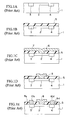
- silicon is introduced into an active region of a GaAs substrate 1 by ion implantation and activated in order to form an n-GaAs layer 2, followed by formation of n +- GaAs layers 3 and 4 on both sides of the GaAs layer 2 by the same manner.
- An insulating layer 5 consisting of a silicon oxide film, a silicon nitride film or the like is then formed on the GaAs substrate 1 by plasma CVD as illustrated in Fig.1 B.
- the insulating layer 5 is then patterned by photolithography in order to form an opening 6 in a location just over the n-GaAs layer 2, followed by formation of a tungsten silicide layer (WSi layer) 7 on the insulating layer 5 and in the opening 6 by sputtering as illustrated in Fig.1 C.
- the WSi layer 7 is formed to make schottky contact with the n-GaAs layer 2.
- the GaAs substrate 1 is heated in order to recover the crystallinity of the surface portion of the GaAs substrate 1,which has been damaged by the previous plasma CVD.
- the temperature of the thermal treatment is about 600 ° C.
- the WSi layer 7 is patterned by photolithography after the thermal treatment in order to leave it only the area in the opening 6 and the periphery thereof as illustrated in Fig.1 D, thus forming a gate electrode 8 of a T shape.
- a source electrode 10s and a drain electrode 10d are formed to make ohmic contact with the n +- GaAs layers 3 and 4 through the openings 9s and 9d.
- the variation of threshold voltage originates from the thermal treatment given at 600 °C to the GaAs substrate 1 in which the n-GaAs layer 2 makes schottky contact with the WSi layer 7 formed on the insulating layer 5 through the opening 6. This problem may arise also in the case of manufacturing an HEMT.
- the variation of threshold voltage of transistors may be avoided by lowering the temperature of the thermal treatment.
- the crystallinity of the semiconductor layer making schottky contact with the gate electrode can not be sufficiently recovered at a low temperature so that a reverse breakdown voltage to the gate electrode is decreased and therefore breakdown may frequently occur.
- the present invention has been made in order to solve the shortcomings as described above.
- an insulating layer is formed on a semiconductor layer containing an impurity.
- the semiconductor layer is damaged during formation of the insulating layer to degrade the crystallinity thereof.
- the crystallinity of the semiconductor layer is therefore recovered after the formation of the insulating layer by heating it at a first temperature.
- a first opening is formed through the insulating layer.
- a conductive layer capable of making schottky contact with the semiconductor layer is formed within the first opening.
- the semiconductor layer is then heated at a second temperature lower than the first temperature in order to recover the damage due to formation of the conductive layer.
- the first temperature is higher than 550 °C while the second temperature is no lower than 400 °C and no higher than 550 °C.
- the semiconductor layer is made from an n-type GaAs, or any other compound semiconductors.
- the insulating layer is a single-layered structure made from either of silicon oxide and silicon nitride or a dual-layered structure made from a silicon nitride layer and a silicon oxide layer.
- a semiconductor layer is heated by a first thermal treatment after an insulating layer is formed on the semiconductor layer, and heated by a second thermal treatment after formation of a conductive layer in an opening formed through the insulating layer.
- the crystallinity of the semiconductor layer is recovered by these two thermal treatments.
- the damage imparted to the semiconductor layer during formation of the insulating layer is recovered by the first thermal treatment.
- the damage imparted to the semiconductor layer during formation of the conductive layer and the opening is recovered by the second thermal treatment.
- the temperature of the first treatment is set higher than that of the second thermal treatment. For example, the temperature of the first thermal treatment is higher than 550 °C while the temperature of the second thermal treatment is no lower than 400 °C and no higher than 550 ° C.
- the damage imparted to the semiconductor layer during formation of the insulating layer is removed by recrystallization caused by the relatively high temperature during the first thermal treatment.
- the damage of the surface portion of the semiconductor layer is removed by the high temperature thermal treatment so as to increase the breakdown voltage as compared with those of conventional "T"-shaped gate devices.
- the temperature of the second thermal treatment is selected to be relatively low in order to decrease the stress due to heat applied to the conductive layer and the insulating layer. If the stress strongly appears, the threshold voltage of semiconductor devices becomes substantially dispersed. Accordingly, equality of the threshold voltage is maintained by lowering the temperature of the second thermal treatment.
- the surface portion of the semiconductor layer is removed by etching. Also, in order to decrease lattice defects just below the opening, it is effective to utilize wet etching for forming the opening.
- the introduction of an impurity into the semiconductor layer can be performed at the same time as the formation of the semiconductor layer or after the formation of the semiconductor layer by ion implantation.
- the method for manufacturing semiconductor devices in accordance with the present invention is applicable for MESFETs or HEMTs having "T"- shaped gate electrodes.
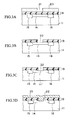
- Figs.2 through 4 are cross sectional views showing the method for forming a MESFET in accordance with a first embodiment of the present invention.
- silicon is introduced into an active region 12 of a semi-insulating gallium arsenic (GaAs) substrate 11 by ion implantation.
- the ion implantation is carried out in two steps. The first step is performed in the entirety of the active region 12 with an acceleration energy of 60 keV and a dose amount of 4x 10' 2 /cm 2 .
- the second step is performed in the both sides of the active region 12 with an acceleration energy of 120 keV and a dose amount of 2x 10 13 /cm 2 .
- the surface of the GaAs substrate 11 is then coated with a silicon oxide (Si0 2 ) film 13 by CVD followed by giving thermal treatment at about 800 °C in order to activate the silicon introduced into the GaAs substrate 11.
- a silicon oxide (Si0 2 ) film 13 by CVD followed by giving thermal treatment at about 800 °C in order to activate the silicon introduced into the GaAs substrate 11.
- n-GaAs region 14 serving as a channel region
- n +- GaAs regions 15 and 16 serving as contact regions (source and drain regions).
- the activation of the silicon may be carried out after formation of an insulating layer 19 (described supra) depending upon the actual case in practice.
- the temperature of the thermal treatment is no lower than 800 ° C in this case.
- a silicon nitride (SiN) layer 17 and a silicon oxide (Si0 2 ) layer 18 are formed on the GaAs substrate 11 respectively to a thickness of 100nm and a thickness of 200nm by plasma CVD to form an insulating layer 19 as illustrated in Fig.2C.
- the SiN layer 17 is grown with a growth gas of SiH 4 and N 2 at a growth temperature of 300 ° C in a pressure of about 1 Torr.
- the Si0 2 layer 18 is grown with a growth gas of SiH 4 and 0 2 at a growth temperature of 300 ° C in a pressure of 1 Torr.
- the SiN layer 17 is particularly suitable for forming a passivation film while the Si0 2 layer 18 is more appropriate than the SiN layer 17 in term of causing weaker stress.
- the insulating layer 19 is not limited to such a dual layered structure but also can be formed only of either one of the SiN layer 17 and the Si0 2 layer 18 or formed of another film such as a silicon nitride oxide (SiON) film.
- the GaAs substrate 11 is heated at a temperature of higher than 550 °C for about 30 minutes as illustrated in Fig.2D.
- the crystallinity of the surface of the GaAs substrate 11 is recovered from the substantial damage received due to plasma CVD.
- a resist film 20 is coated on the GaAs substrate 11 and then patterned to from an opening 21 through exposure and development, as illustrated in Fig.3A, in a location where a gate electrode is to be formed.
- RIE reactive ion etching
- the surface portion of the n-GaAs region 14 is subjected to wet etching to form a recess 22' to a depth of 10 to 20 nm.
- a recess structure is thus formed on the n-GaAs region 14.
- the etchant solution utilized in this process is, for example, a solution containing hydrofluoric acid and hydrogen peroxide.
- a tungsten silicide layer 23 is formed on the insulating layer 19 and in the opening 22 as illustrated in Fig.3D.
- the GaAs substrate 11 is then heated at 400 to 550 °C for about 30 minutes in order to recover the crystallinity of the GaAs substrate 11 in which lattice defects have occurred during formation of the opening 22 and the WSi layer 23.
- a titanium (Ti) layer 24 and a gold (Au) layer 25 are deposited on the WSi layer 23 by sputtering in this order, followed by patterning the Ti layer 24, the Au layer 25 and the WSi layer 23 to leave the three layers only in the periphery of the opening 22 and the inside of the opening 22.
- a "T"-shaped gate electrode 26 in schottky contact with the n-GaAs region 14 through the opening 22 is formed by this process, as illustrated in Fig. 4C.
- the insulating layer 19 is patterned to form openings 27 and 28 to expose the n +- GaAs regions 15 and 16.
- the upper surface of the structure is covered by a resist film (not shown in the figure) except for the exposed surfaces of the n +- GaAs regions 15 and 16.
- the entire surface of the structure is then coated with a triple-layered conductive film (not shown in the figure) consisting of a gold-germanium (AuGe) film, an nickel (Ni) film and gold (Au) film disposed in this order.
- the resist film is then removed to pattern the triple-layered conductive film by the lift-off technique.
- a source and a drain electrodes 29 and 30 are formed making contact with the n +- GaAs regions 15 and 16 respectively through the openings 27 and 28.
- the MESFET is then substantially completed.
- n-GaAs region 14 and the n +- GaAs regions 15 and 16 can be formed within a GaAs layer epitaxially grown on the GaAs substrate 11.
- thermal treatment is performed in two steps at different temperatures before and after the formation of the WSi layer 23 serving as a gate electrode 26 in the manufacturing process of the MESFET.
- the GaAs substrate 11 is heated, for example, at 650 °C before the formation of the WSi layer 23 on the GaAs substrate 11 and at 500 °C after the formation of the WSi layer 23 on the GaAs substrate 11.
- the variation of threshold voltage of transistors was limited and the withstand voltage (breakdown voltage) between the gate electrode and the drain electrode is improved.
- the inventors of the present invention conducted an comparative experiment in which thermal treatment was performed only after the formation of the WSi layer 23 for recovery of the crystallinity of the semiconductor layer of the GaAs substrate 11 in the manufacture process as illustrated in Figs.lA to 1E.
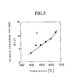
- the variation of threshold voltage of transistors and the reverse breakdown voltage Vr applied on the gate electrode were measured while the temperature of the thermal treatment is varied.
- Figs.5 to 7 are graphical diagrams in which the measurement results are plotted.
- the breakdown voltage Vr to the gate electrode was increased as the temperature of thermal treatment was elevated.
- the variation of threshold voltage of transistors was widened as the temperature of thermal treatment was elevated.
- variation of the drain saturation current I dss which has been measured by setting the gate voltage to be 0 and the drain voltage to be 3V, was increased as the temperature of thermal treatment was elevated.
- the abscissa of the diagram in Fig.6 represents the standard deviation 6vth of the threshold voltage while the vertical line passing through solid circles in the direction of the abscissa of the diagram in Fig.7 represent the respective standard deviations of the drain saturation current.
- Breakdown due to the reverse voltage applied to the gate electrode easily occurs near lattice defects.
- lattice defects caused during formation of the insulating layer 19 on the surface of the GaAs substrate 11 tend to form a current path, resulting in breakdown. Namely, the lattice defects on the surface of the GaAs substrate 11 often become the cause of breakdown. Accordingly, when the gate voltage is 7V, recrystallization of the surface portion of the GaAs substrate 11 can not be dispensed with, as will be understood from Fig.5.
- the temperature for the recrystallization is preferably no higher than, e.g., 900 ° C.
- the recrystallization temperature In order to suppress the variation of the threshold voltage, the recrystallization temperature must be lowered as will be understood from Figs.6 and 7.
- the thermal treatment When it is desired to limit the standard deviation ⁇ Vth below 0.2V and the drain saturation current I dss below 100mA/mm, the thermal treatment must be carried out at a temperature no higher than 550 ° C as will be understood from Figs.6 and 7. Since it is difficult to perform recrystallization at a temperature no higher than 400 °C in practice, the thermal treatment is carried out at a temperature no lower than 400 ° C and no higher than 550 ° C to perform recrystallization.
- thermal treatment at a temperature no lower than 550 ° C can be performed before the formation of the WSi layer 23 serving as a gate electrode 26 in order to avoid the generation of lattice defects in the surface portion of the GaAs substrate 11 and minimize the thermal stress applied to the gate electrode 26 and the insulating layer 19.
- the GaAs substrate 11 when the GaAs substrate 11 is recrystallized to remove lattice defects caused during formation of the opening 22 of the insulating layer 19 or formation of the WSi layer 23, thermal treatment is given to the GaAs substrate 11 after the formation of the WSi layer 23 at a temperature no lower than 400 ° C and no higher than 550 ° C to perform recrystallization of the GaAs substrate 11.
- the crystallinity of the GaAs substrate 11 is usually sufficient by thermal treatment at the temperature no lower than 400 °C and no higher than 550 °C. However, if the recovery of crystallinity near the surface of the GaAs substrate 11 is not sufficient, the surface portion of the GaAs substrate 11 is removed as described above.
- the crystallinity of the GaAs substrate 11 is improved by thermal treatment at 650 °C after formation of the insulating layer 19.
- the reverse breakdown voltage Vr to the gate electrode could be expected to be about 11 V by the thermal treatment at 650 °C as illustrated in Fig. 5.
- the crystallinity of the GaAs substrate 11 is improved again by thermal treatment at 460 °C after formation of the WSi layer 23 on the insulating layer 19.
- the drain saturation current I dss was about 11 OmA/mm only with a limited standard deviation as illustrated in Fig.7 with an open circle.
- the reverse breakdown voltage was measured after thermal treatment at 460 °C, the result of measurement was about 11 V in agreement with that expected from the open circle in Fig.5.
- thermal treatment can be performed at a temperature no lower than 620 ° C before the formation of the WSi layer 23 and at a temperature no lower than 400 °C to 550 ° C after the formation of the WSi layer 23 to meet the requirements.
- Fig.8 illustrates one example of such a MESFET provided with an n-GaAs layer 34 epitaxially grown on a semi-insulating GaAs substrate 31 through an n-GaAs layer 32 and an AIGaAs buffer layer 33.
- the reverse breakdown voltage Vr and the variation of the threshold voltage can be improved also in this case.
- the same numerals are given to similar elements also in Fig.8 as compared with Figs.2 to 4.
- the thermal treatment performed in two steps at different temperatures before and after the formation of the conductive layer serving as a gate electrode can be applied for the manufacturing process of the HEMT having a "T"-shaped gate electrode as illustrated in Fig.9.
- the reverse breakdown voltage and the variation of the threshold voltage can be improved also in this case.
- a un-doped GaAs layer 42, an n-AIGaAs layer 43 and an insulating layer 44 are formed on a semi-insulating GaAs substrate 41 in this order.
- First to third openings 45 to 47 are formed through the insulating layer 44.
- a "T"- shaped gate electrode 48 is formed in the first opening 45, making schottky contact with the n-AIGaAs layer 43.
- a source electrode 49 and a drain electrode 50 are formed, making ohmic contact with the n-AIGaAs layer 43 respectively through the second opening 46 and the third opening 47.
- Two dimensional electron gas exists near the junction between the un-doped GaAs layer 42 and the n-AIGaAs layer 43.
- a recess 52 is formed in the n-AIGaAs layer 43 just below the gate electrode 48.
- the description of the above embodiments have been made to the MESFET provided with the gate electrode made from WSi.
- the gate electrode can be made from aluminum, tungsten titanium and so forth instead.
- the description of the above embodiments have been made to the MESFET provided with the semiconductor layer serving as a channel region made from GaAs.
- other semiconductors such as an InGaAs can be utilized for the same purpose.
- a un-doped InGaAs layer can be used in place of the un-doped GaAs layer while an InGaP layer, an InGaAs layer and the like doped with an n-type impurity can be utilized in place of the n-AIGaAs layer.
- N-type impurities available for forming n-type compound semiconductors include, for example, selenium and tin besides silicon as employed in the above.
Landscapes
- Junction Field-Effect Transistors (AREA)
Applications Claiming Priority (2)
| Application Number | Priority Date | Filing Date | Title |
|---|---|---|---|
| JP6112837A JPH07321128A (ja) | 1994-05-26 | 1994-05-26 | 半導体装置の製造方法 |
| JP112837/94 | 1994-05-26 |
Publications (2)
| Publication Number | Publication Date |
|---|---|
| EP0684633A2 true EP0684633A2 (fr) | 1995-11-29 |
| EP0684633A3 EP0684633A3 (fr) | 1997-06-04 |
Family
ID=14596779
Family Applications (1)
| Application Number | Title | Priority Date | Filing Date |
|---|---|---|---|
| EP95105463A Withdrawn EP0684633A3 (fr) | 1994-05-26 | 1995-04-11 | Méthode de fabrication d'un dispositif semi-conducteur. |
Country Status (2)
| Country | Link |
|---|---|
| EP (1) | EP0684633A3 (fr) |
| JP (1) | JPH07321128A (fr) |
Cited By (1)
| Publication number | Priority date | Publication date | Assignee | Title |
|---|---|---|---|---|
| FR2758207A1 (fr) * | 1997-01-07 | 1998-07-10 | Fujitsu Ltd | Procede de fabrication d'un dispositif a semiconducteur composite haute vitesse presentant une capacite et une resistance parasites minimisees et un hemt, un mesfet et un hbt selon ce procede |
-
1994
- 1994-05-26 JP JP6112837A patent/JPH07321128A/ja active Pending
-
1995
- 1995-04-11 EP EP95105463A patent/EP0684633A3/fr not_active Withdrawn
Non-Patent Citations (2)
| Title |
|---|
| INTERNATIONAL CONFERENCE ON SOLID STATE DEVICES AND MATERIALS, 1 August 1992, pages 573-575, XP000312270 YOHTARO UMEDA ET AL: "HIGH-PERFORMANCE INALAS/INGAAS HEMTS AND THEIR APPLICATION TO A 40-GHZ MONOLITHIC AMPLIFIER" * |
| MICROELECTRONIC ENGINEERING, vol. 18, no. 3, 1 August 1992, pages 215-223, XP000334737 YA-MIN LEE J ET AL: "A NOVEL LIFT-OFF PROCESS USING LOW-TEMPERATURE PECVD SILICON NITRIDE FOR THE FABRICATION OF SELF-ALIGNED GATE GAAS MESFETS AND INP MISFETS" * |
Cited By (3)
| Publication number | Priority date | Publication date | Assignee | Title |
|---|---|---|---|---|
| FR2758207A1 (fr) * | 1997-01-07 | 1998-07-10 | Fujitsu Ltd | Procede de fabrication d'un dispositif a semiconducteur composite haute vitesse presentant une capacite et une resistance parasites minimisees et un hemt, un mesfet et un hbt selon ce procede |
| US5939737A (en) * | 1997-01-07 | 1999-08-17 | Fujitsu Limited | High-speed compound semiconductor device having a minimized parasitic capacitance and resistance |
| US6586319B1 (en) | 1997-01-07 | 2003-07-01 | Fujitsu Limited | High-speed compound semiconductor device having a minimized parasitic capacitance and resistance |
Also Published As
| Publication number | Publication date |
|---|---|
| JPH07321128A (ja) | 1995-12-08 |
| EP0684633A3 (fr) | 1997-06-04 |
Similar Documents
| Publication | Publication Date | Title |
|---|---|---|
| US5041393A (en) | Fabrication of GaAs integrated circuits | |
| US4711858A (en) | Method of fabricating a self-aligned metal-semiconductor FET having an insulator spacer | |
| US5614739A (en) | HIGFET and method | |
| EP0283278A2 (fr) | Composé semi-conducteur à contacts ohmiques sans alliage | |
| EP0631324A1 (fr) | Procédé pour la fabrication de contacts chimique pour des dispositifs à semi-conducteurs complémentaires | |
| EP0631323A1 (fr) | Dispositif semi-conducteur III-V complémentaire à structure hétérogène avec des contacts chimiques compatibles sans or | |
| US4679311A (en) | Method of fabricating self-aligned field-effect transistor having t-shaped gate electrode, sub-micron gate length and variable drain to gate spacing | |
| JP3233207B2 (ja) | 電界効果トランジスタの製造方法 | |
| KR900005560B1 (ko) | 반도체장치 및 그 제조방법 | |
| JPH11354541A (ja) | 半導体装置およびその製造方法 | |
| EP0244840B1 (fr) | Procédé pour la fabrication d'un MESFET | |
| US5693544A (en) | N-type higfet and method | |
| JP3187764B2 (ja) | GaAsを基本としたMOSFET及びその製品 | |
| US5411903A (en) | Self-aligned complementary HFETS | |
| EP0684633A2 (fr) | Méthode de fabrication d'un dispositif semi-conducteur | |
| US4895811A (en) | Method of manufacturing semiconductor device | |
| US5837570A (en) | Heterostructure semiconductor device and method of fabricating same | |
| JPH0750781B2 (ja) | 化合物半導体集積回路装置 | |
| JPH0249012B2 (fr) | ||
| JP2817217B2 (ja) | 金属・半導体接合を有する半導体装置およびその製造方法 | |
| JPS6038882A (ja) | シヨツトキゲ−ト型fetの製造方法 | |
| JPS6143443A (ja) | 半導体装置の製造方法 | |
| JP3347837B2 (ja) | 化合物半導体電界効果トランジスタ | |
| JP4186267B2 (ja) | 化合物半導体装置の製造方法 | |
| JP2000323429A (ja) | 半導体装置およびその製造方法 |
Legal Events
| Date | Code | Title | Description |
|---|---|---|---|
| PUAI | Public reference made under article 153(3) epc to a published international application that has entered the european phase |
Free format text: ORIGINAL CODE: 0009012 |
|
| AK | Designated contracting states |
Kind code of ref document: A2 Designated state(s): DE FR GB |
|
| PUAL | Search report despatched |
Free format text: ORIGINAL CODE: 0009013 |
|
| AK | Designated contracting states |
Kind code of ref document: A3 Designated state(s): DE FR GB |
|
| 17P | Request for examination filed |
Effective date: 19971125 |
|
| 17Q | First examination report despatched |
Effective date: 19990512 |
|
| STAA | Information on the status of an ep patent application or granted ep patent |
Free format text: STATUS: THE APPLICATION IS DEEMED TO BE WITHDRAWN |
|
| 18D | Application deemed to be withdrawn |
Effective date: 19990923 |