EP0685885B1 - Verbesserungen in Bezug auf die Herstellung von Halbleitervorrichtungen - Google Patents
Verbesserungen in Bezug auf die Herstellung von Halbleitervorrichtungen Download PDFInfo
- Publication number
- EP0685885B1 EP0685885B1 EP95303615A EP95303615A EP0685885B1 EP 0685885 B1 EP0685885 B1 EP 0685885B1 EP 95303615 A EP95303615 A EP 95303615A EP 95303615 A EP95303615 A EP 95303615A EP 0685885 B1 EP0685885 B1 EP 0685885B1
- Authority
- EP
- European Patent Office
- Prior art keywords
- layer
- metal leads
- porous dielectric
- disposable solid
- metal
- Prior art date
- Legal status (The legal status is an assumption and is not a legal conclusion. Google has not performed a legal analysis and makes no representation as to the accuracy of the status listed.)
- Expired - Lifetime
Links
Images



Classifications
-
- H—ELECTRICITY
- H10—SEMICONDUCTOR DEVICES; ELECTRIC SOLID-STATE DEVICES NOT OTHERWISE PROVIDED FOR
- H10P—GENERIC PROCESSES OR APPARATUS FOR THE MANUFACTURE OR TREATMENT OF DEVICES COVERED BY CLASS H10
- H10P14/00—Formation of materials, e.g. in the shape of layers or pillars
- H10P14/60—Formation of materials, e.g. in the shape of layers or pillars of insulating materials
- H10P14/69—Inorganic materials
- H10P14/692—Inorganic materials composed of oxides, glassy oxides or oxide-based glasses
- H10P14/6921—Inorganic materials composed of oxides, glassy oxides or oxide-based glasses containing silicon
- H10P14/6922—Inorganic materials composed of oxides, glassy oxides or oxide-based glasses containing silicon the material containing Si, O and at least one of H, N, C, F or other non-metal elements, e.g. SiOC, SiOC:H or SiONC
-
- H—ELECTRICITY
- H10—SEMICONDUCTOR DEVICES; ELECTRIC SOLID-STATE DEVICES NOT OTHERWISE PROVIDED FOR
- H10P—GENERIC PROCESSES OR APPARATUS FOR THE MANUFACTURE OR TREATMENT OF DEVICES COVERED BY CLASS H10
- H10P14/00—Formation of materials, e.g. in the shape of layers or pillars
- H10P14/60—Formation of materials, e.g. in the shape of layers or pillars of insulating materials
- H10P14/63—Formation of materials, e.g. in the shape of layers or pillars of insulating materials characterised by the formation processes
- H10P14/6326—Deposition processes
- H10P14/6342—Liquid deposition, e.g. spin-coating, sol-gel techniques or spray coating
-
- H—ELECTRICITY
- H10—SEMICONDUCTOR DEVICES; ELECTRIC SOLID-STATE DEVICES NOT OTHERWISE PROVIDED FOR
- H10P—GENERIC PROCESSES OR APPARATUS FOR THE MANUFACTURE OR TREATMENT OF DEVICES COVERED BY CLASS H10
- H10P14/00—Formation of materials, e.g. in the shape of layers or pillars
- H10P14/60—Formation of materials, e.g. in the shape of layers or pillars of insulating materials
- H10P14/65—Formation of materials, e.g. in the shape of layers or pillars of insulating materials characterised by treatments performed before or after the formation of the materials
- H10P14/6502—Formation of materials, e.g. in the shape of layers or pillars of insulating materials characterised by treatments performed before or after the formation of the materials of treatments performed before formation of the materials
- H10P14/6506—Formation of intermediate materials
-
- H—ELECTRICITY
- H10—SEMICONDUCTOR DEVICES; ELECTRIC SOLID-STATE DEVICES NOT OTHERWISE PROVIDED FOR
- H10P—GENERIC PROCESSES OR APPARATUS FOR THE MANUFACTURE OR TREATMENT OF DEVICES COVERED BY CLASS H10
- H10P14/00—Formation of materials, e.g. in the shape of layers or pillars
- H10P14/60—Formation of materials, e.g. in the shape of layers or pillars of insulating materials
- H10P14/65—Formation of materials, e.g. in the shape of layers or pillars of insulating materials characterised by treatments performed before or after the formation of the materials
- H10P14/6516—Formation of materials, e.g. in the shape of layers or pillars of insulating materials characterised by treatments performed before or after the formation of the materials of treatments performed after formation of the materials
- H10P14/6529—Formation of materials, e.g. in the shape of layers or pillars of insulating materials characterised by treatments performed before or after the formation of the materials of treatments performed after formation of the materials by exposure to a gas or vapour
-
- H—ELECTRICITY
- H10—SEMICONDUCTOR DEVICES; ELECTRIC SOLID-STATE DEVICES NOT OTHERWISE PROVIDED FOR
- H10P—GENERIC PROCESSES OR APPARATUS FOR THE MANUFACTURE OR TREATMENT OF DEVICES COVERED BY CLASS H10
- H10P14/00—Formation of materials, e.g. in the shape of layers or pillars
- H10P14/60—Formation of materials, e.g. in the shape of layers or pillars of insulating materials
- H10P14/65—Formation of materials, e.g. in the shape of layers or pillars of insulating materials characterised by treatments performed before or after the formation of the materials
- H10P14/6516—Formation of materials, e.g. in the shape of layers or pillars of insulating materials characterised by treatments performed before or after the formation of the materials of treatments performed after formation of the materials
- H10P14/6548—Formation of materials, e.g. in the shape of layers or pillars of insulating materials characterised by treatments performed before or after the formation of the materials of treatments performed after formation of the materials by forming intermediate materials, e.g. capping layers or diffusion barriers
-
- H—ELECTRICITY
- H10—SEMICONDUCTOR DEVICES; ELECTRIC SOLID-STATE DEVICES NOT OTHERWISE PROVIDED FOR
- H10P—GENERIC PROCESSES OR APPARATUS FOR THE MANUFACTURE OR TREATMENT OF DEVICES COVERED BY CLASS H10
- H10P14/00—Formation of materials, e.g. in the shape of layers or pillars
- H10P14/60—Formation of materials, e.g. in the shape of layers or pillars of insulating materials
- H10P14/66—Formation of materials, e.g. in the shape of layers or pillars of insulating materials characterised by the type of materials
- H10P14/665—Porous materials
-
- H—ELECTRICITY
- H10—SEMICONDUCTOR DEVICES; ELECTRIC SOLID-STATE DEVICES NOT OTHERWISE PROVIDED FOR
- H10W—GENERIC PACKAGES, INTERCONNECTIONS, CONNECTORS OR OTHER CONSTRUCTIONAL DETAILS OF DEVICES COVERED BY CLASS H10
- H10W20/00—Interconnections in chips, wafers or substrates
- H10W20/01—Manufacture or treatment
- H10W20/071—Manufacture or treatment of dielectric parts thereof
- H10W20/072—Manufacture or treatment of dielectric parts thereof of dielectric parts comprising air gaps
-
- H—ELECTRICITY
- H10—SEMICONDUCTOR DEVICES; ELECTRIC SOLID-STATE DEVICES NOT OTHERWISE PROVIDED FOR
- H10W—GENERIC PACKAGES, INTERCONNECTIONS, CONNECTORS OR OTHER CONSTRUCTIONAL DETAILS OF DEVICES COVERED BY CLASS H10
- H10W20/00—Interconnections in chips, wafers or substrates
- H10W20/40—Interconnections external to wafers or substrates, e.g. back-end-of-line [BEOL] metallisations or vias connecting to gate electrodes
- H10W20/45—Interconnections external to wafers or substrates, e.g. back-end-of-line [BEOL] metallisations or vias connecting to gate electrodes characterised by their insulating parts
- H10W20/46—Interconnections external to wafers or substrates, e.g. back-end-of-line [BEOL] metallisations or vias connecting to gate electrodes characterised by their insulating parts comprising air gaps
-
- H—ELECTRICITY
- H10—SEMICONDUCTOR DEVICES; ELECTRIC SOLID-STATE DEVICES NOT OTHERWISE PROVIDED FOR
- H10W—GENERIC PACKAGES, INTERCONNECTIONS, CONNECTORS OR OTHER CONSTRUCTIONAL DETAILS OF DEVICES COVERED BY CLASS H10
- H10W20/00—Interconnections in chips, wafers or substrates
- H10W20/40—Interconnections external to wafers or substrates, e.g. back-end-of-line [BEOL] metallisations or vias connecting to gate electrodes
- H10W20/495—Capacitive arrangements or effects of, or between wiring layers
Definitions
- This invention relates generally to the fabrication of semiconductor devices, and more specifically to using air gaps as a low-dielectric constant material between metal leads.
- Semiconductors are widely used in integrated circuits for electronic applications, including radios and televisions. Such integrated circuits typically use multiple transistors fabricated in single crystal silicon. Many integrated circuits now contain multiple levels of metallization for interconnections. The need to integrate more functions onto a chip has caused the semiconductor industry to search for ways to shrink, or scale, the size of individual transistors and other devices commonly integrated on a chip. However, scaling devices to smaller dimensions can create a multitude of undesirable effects. One of these effects is an increase in the capacitive coupling between conductors in a circuit. Therefore, it becomes imperative to reduce the RC time constant within today's multi-level metallization systems.
- the capacitance between conductors is highly dependent on the insulator, or dielectric, used to separate them.
- Conventional semiconductor fabrication commonly employs silicon dioxide as a dielectric, which has a dielectric constant of about 3.9.
- the lowest possible, or ideal, dielectric constant is 1.0, which is the dielectric constant of a vacuum, whereas air has a dielectric constant of less than 1.001.
- EP-A-0 501 407 shows a metallization system using air as dielectric.
- EP-A-0 333 132 shows a metallization system using a porous dielectric.
- a semiconductor device and method is disclosed herein that forms air gaps between metal leads to provide a composite low-dielectric constant of, e.g., about 1.25 between leads which will substantially reduce the capacitive coupling between conductors in a circuit.
- the present invention includes a method for forming air gaps between metal leads of a semiconductor device and semiconductor device structure for same.
- a metal layer is deposited on a substrate.
- the metal layer is etched to form metal leads.
- a disposable solid layer is formed between the metal leads.
- a porous dielectric layer is deposited on the disposable solid layer and the metal leads. The disposable solid layer is removed through the porous dielectric layer to form air gaps between the metal leads beneath the porous dielectric layer.
- a metal layer is deposited on a substrate, and a first oxide layer is deposited on the metal layer.
- the first oxide layer and the metal layer are etched to form etched oxide and metal leads, leaving portions of the substrate exposed.
- a disposable solid layer is deposited on the etched oxide, metal leads and exposed portions of the substrate.
- a top portion of the disposable solid layer is removed to lower the disposable solid layer from at least the tops of the etched oxide.
- a porous dielectric layer is deposited on the disposable solid layer and at least the tops of the etched oxide. The disposable solid layer is removed through the porous dielectric layer to form air gaps between the metal leads and portions of the etched oxide beneath the porous dielectric layer.
- An advantage of the invention includes a novel method of forming air gaps between metal leads.
- the air gaps have a low-dielectric constant and result in reduced sidewall capacitance of the metal leads.
- a further advantage of another preferred embodiment is increasing the process margin by having a relatively thick second oxide layer on top of the metal leads, which allows for a thicker formation of the disposable solid layer. Also, an air gap may be formed near the tops and top corners of the metal leads, to reduce fringing capacitance between leads.
- TEOS Tetraethoxysilane
- PETEOS Plasma-enhanced TEOS
- BPSG boron phosphate silicate glass
- Photoresist Disposable Solid Layer Polymers such as polyimide, parylene or, Teflon; electronresist; solid organics or inorganics; BCB (bisbenzocyclobutene); PMMA (poly-[methyl methacrylate]).
- Silicon dioxide-based xerogel Porous dielectric layer Aerogels Spin-on materials with pores large enough for CO 2 gas or liquids to move through.
- Air gaps "Air", as used herein, may include voids, inert gases or vacuum.
- PETEOS Non-porous dielectric layer SOG, Si 3 N 4 (silicon nitride) 26 Passivating layer Oxide or nitride layer (e.g. conformal); SiO 2 deposited by plasma at low temperature; SACVD or LPCVD oxide layer; plasma-enhanced nitride layer. 28 SiO 2 Etched portions of second oxide layer CVD oxide layer
- Figure 1A shows a cross-sectional view of a semiconductor wafer upon which a first preferred embodiment of the present invention will be performed.
- the semiconductor wafer 10 has a substrate 12 which may, for example, contain transistors, diodes, and other semiconductor elements (not shown) as are well known in the art.
- the substrate 12 may also contain metal interconnect layers.
- First oxide layer 14 has been deposited over the substrate 12 and comprises TEOS (tetraethosiloxane).
- First oxide layer 14 could also comprise PETEOS (plasma-enhanced tetraethosiloxane), BPSG (boron phosphate silicate glass) or other dielectric materials.
- a metal interconnect layer has been deposited over first oxide layer 14 .
- the metal interconnect layer preferably comprises aluminum, but may, for example, comprise a titanium-tungsten/aluminum bilayer or other metal.
- the metal interconnect layer has been etched in a predetermined pattern to form etch lines, or metal leads 16 .
- FIG 1B shows the wafer 10 after a disposable solid layer 18 has been deposited over metal leads 16 and first oxide layer 14 .
- Disposable solid layer 18 is generally a polymer, preferably photoresist, but could also be other polymers such as polyimide, parylene, Teflon, or BCB.
- the top of disposable solid layer is then removed (e.g. etched back) to expose at least the tops of the metal leads 16 , as shown in Figure 1C .
- Porous dielectric layer 20 is deposited on disposable solid layer 18 and at least tops of metal leads 16 , as shown in Figure 1D .
- Porous dielectric layer 20 is preferably comprised of a silica-based xerogel with a 10-50% porosity, although other materials with pores large enough for the molecules of the disposable solid layer 18 to move through may also be used. It is also preferable for the material used in disposable solid layer 18 to decompose in oxygen (this can be e.g. air or some other oxygen-containing atmosphere, or including an oxygen plasma or ozone).
- oxygen this can be e.g. air or some other oxygen-containing atmosphere, or including an oxygen plasma or ozone.
- the porous dielectric layer 20 may be planarized. Then the disposable solid layer 18 is removed through the porous dielectric layer 20 to form air gaps 22 as shown in Figure 1E .
- the removal of the disposable solid layer 18 is preferably accomplished by exposing the wafer to oxygen or oxygen-plasma at a high temperature (typically >100°C), to vaporize, or burn off the photoresist.
- the oxygen moves through the porous dielectric layer 20 to reach the disposable solid layer 18 and react with solid layer 18 and convert it to a gas that moves back out of porous dielectric layer 20 .
- the photoresist reacts with the oxygen to form gaseous byproducts, including either CO 2 or CO.
- the photoresist vaporizes (the reaction products of the solid form a gas).
- non-porous dielectric layer 24 is deposited on top of the porous dielectric layer 20 as shown in Figure 1F .
- the non-porous dielectric layer is preferably a CVD oxide, which seals the porous dielectric layer 20 from moisture, provides improved structural support and thermal conductivity, and passivates the porous dielectric layer 20 .
- Subsequent processing steps may then be performed (not shown), e.g. planarization of non-porous dielectric layer 24 , or further deposition and etching of semiconductor, insulative and metallic layers.
- a second embodiment is shown in Figure 2 .
- the metal leads 16 have been formed directly on the substrate 12 , and the subsequent steps of the invention as described for the first embodiment are then performed.
- the substrate 12 may comprise an insulator.
- a flow chart for the first and second embodiments shown in Figures 1 and 2 is shown in Figure 3 .
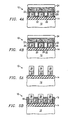
- FIG. 4A shows a third embodiment of the present invention in which a (for example, conformal) passivating layer 26 passivates both exposed surfaces of first oxide layer 14 and prevents interlead leakage.
- a fourth embodiment involves exposing the metal leads to a gas to react and form a passivating layer only around metal leads 16 .
- FIG. 5A shows a cross-sectional view of a semiconductor wafer upon which this embodiment of the present invention will be performed.
- First oxide layer 14 has been deposited over the substrate 12 of semiconductor wafer 10 .
- a metal interconnect layer has been deposited over first oxide layer 14
- a second oxide layer has been deposited over the metal interconnect layer.
- the thickness of this second oxide layer is preferably about 50-100% the height of the metal interconnect layer.
- the second oxide layer and the metal interconnect layer are etched (generally in separate etch steps) in a predetermined pattern to form etch lines, or metal leads 16 with etched portions 28 of second oxide layer remaining on top of metal leads 16 .
- a disposable solid layer 18 is deposited over etched portions 28 of second oxide layer and metal leads 16 .
- the disposable solid layer 18 is then removed (e.g. etched back) to expose at least the tops of the etched portions 28 of second oxide layer, as shown in Figure 5B .
- Preferably, 70-90% (but also suitably, 60-100%) of the etched portion 28 of second oxide layer remains covered with disposable solid layer 18 after the etch-back step.
- Porous dielectric layer 20 is deposited on disposable solid layer 18 and at least tops of etched portion 28 of second oxide layer, as shown in Figure 5C .
- the porous dielectric layer 20 may be planarized, and then the disposable solid layer 18 is removed through the porous dielectric layer 20 (as described in the first embodiment) to form air gaps 22 .
- non-porous dielectric layer 24 may be deposited on top of the porous dielectric layer 20 as shown in Figure 5D . Subsequent processing steps may then be performed (not shown), e.g. planarization of non-porous dielectric layer 24 , or further deposition and etching of semiconductor, insulative and metallic layers.
- the sixth embodiment includes the fifth embodiment with a passivation layer 26 applied over etched portions 28 of second oxide layer, metal leads 16 , and first oxide layer 14 ( Figures 6A and 6B ), as described for the third embodiment (the metal leads 16 may alternately or also be treated as in Figure 4B ).
- Another method of removing the disposable solid layer 18 may involve introducing a solvent to the wafer, such as acetone.
- the wafer can be agitated to facilitate movement of the solvent through the porous dielectric layer 20 to reach the disposable solid layer 18 .
- the solvent dissolves the polymer 18 and then a vacuum may be utilized to remove the gaseous by-products of the dissolved disposable solid layer 18 through the porous dielectric layer 20 .
- the present invention offers a novel method of forming air gaps between metal leads which is beneficial to semiconductors requiring low-dielectric constant materials.
- the air gaps have a low-dielectric constant and result in reduced sidewall capacitance of the metal leads.
- the fifth embodiment described has the further advantage of increasing the process margin by having a second oxide layer on top of the metal leads, which allows for a thicker formation of the disposable solid layer.
- an air gap may be formed near the tops and top corners of the metal leads, to reduce fringing capacitance from lead to lead. Generally xerogel-type formation of the porous layer is preferred.
- a glass-former such as TEOS
- Such processing involves significant permanent shrinkage (densification) during drying.
- Aerogel-type processing can also be used, which avoids any significant permanent shrinkage and can provide higher porosity (e.g. up to 95% porosity). Although aerogel-type porosity can provide lower interlayer capacitance, the denser layers are better structurally, and are preferred.
Landscapes
- Internal Circuitry In Semiconductor Integrated Circuit Devices (AREA)
Claims (10)
- Verfahren zum Erzeugen von Luftspalten zwischen Metallleiterbahnen eines Halbleiterbausteins, bei demeine Metallschicht auf einem Substrat abgeschieden wird;die Metallschicht in einem vorherbestimmten Muster qeätzt wird, um Metallleiterbahnen zu bilden;eine feste Hilfsschicht zwischen den Metallleiterbahnen gebildet wird;eine poröse dielektrische Schicht auf der festen Hilfsschicht und den Metallleitarbahnen abgeschieden wird; unddie feste Hilfsschicht durch die poröse dielektrische Schicht hindurch entfernt wird, um Luftspalte zwischen den Metallleiterbahnen unter der porösen dielektrischen Schicht zu erzeugen.
- Verfahren nach Anspruch 1, bei dem bei dem Schritt des Bildens einer festen Hilfsschichteine feste Hilfsschicht auf freiliegenden Teilen des Substrats und auf den Metallleiterbahnen abgeschieden wird; undder obere Teil der festen Hilfsschicht entfernt wird, um wenigstens die oberen Bereiche der Metallleiterbahnen freizulegen.
- Verfahren nach Anspruch 1 oder Anspruch 2, bei dem darüber hinaus nach dem Entfernen der festen Hilfsschicht eine nichtporöse dielektrische Schicht auf der porösen dielektrischen Schicht abgeschieden wird.
- Verfahren nach einem der vorhergehenden Ansprüche, bei dem darüber hinaus eine Passivierungsschicht auf wenigstens den Metallleiterbahnen abgeschieden wird, nachdem die Metallschicht in einem vorherbestimmten Muster geätzt wurde, um Metallleiterbahnen zu bilden.
- Verfahren nach Anspruch 4, bei dem bei dem Schritt des Bildens der Passivierungsschicht eine ein Oxid enthaltende Passivierungsschicht gebildet wird.
- verfahren nach einem der vorhergehenden Ansprüche mit Ausnahme des Anspruchs 2, bei dem darüber hinaus nach dem Schritt des Abscheidens einer Metallschicht auf einem Substrat eine Oxidschicht abgeschieden und in einem vorherbestimmten Muster geätzt wird.
- Verfahren nach einem der vorhergehenden Ansprüche, bei dem darüber hinaus die feste Hilfsschicht aus einem Polymer besteht und bei dem Schritt des Entfernens der festen Hilfsschicht durch die poröse dielektrische Schicht hindurch der Wafer in einer Sauerstoffatmosphäre erhitzt wird, um die feste Hilfsschicht zu verdampfen.
- Verfahren nach einem der Ansprüche 1 bis 6, bei dem bei dem Schritt des Entfernens der festen Hilfsschicht durch die poröse dielektrische Schicht hindurchder Wafer in ein Lösungsmittel eingebracht wird, um die feste Hilfsschicht aufzulösen, wobei das Lösungsmittel durch die poröse dielektrische Schicht hindurchläuft; unddie gelöste feste Hilfsschicht durch die poröse dielektrische Schicht hindurch entfernt wird.
- Halbleiterbaustein mit Luftspalten zwischen Metallleiterbahnen mitauf einem Substrat gebildeten Metallleiterbahnen;zwischen wenigstens einem Teil der Metallleiterbahnen gebildeten Luftspalten;einer dielektrischen Schicht, die eine Porosität zwischen 10 und 50 % aufweist und auf den Metallleiterbahnen und über den Luftspalten gebildet ist; undeiner auf der porösen dielektrischen Schicht gebildeten nichtporösen dielektrischen Schicht.
- Halbleiterbaustein nach Anspruch 9, der darüber hinaus ein strukturiertes Oxid auf den Metallleiterbahnen umfaßt, wobei das strukturierte Oxid das gleiche Muster wie die Metallleiterbahnen aufweist und seine Höhe 50-100 % der Höhe der Metallleiterbahnen beträgt.
Applications Claiming Priority (2)
| Application Number | Priority Date | Filing Date | Title |
|---|---|---|---|
| US08/250,063 US5461003A (en) | 1994-05-27 | 1994-05-27 | Multilevel interconnect structure with air gaps formed between metal leads |
| US250063 | 1999-02-12 |
Publications (2)
| Publication Number | Publication Date |
|---|---|
| EP0685885A1 EP0685885A1 (de) | 1995-12-06 |
| EP0685885B1 true EP0685885B1 (de) | 1999-11-17 |
Family
ID=22946169
Family Applications (1)
| Application Number | Title | Priority Date | Filing Date |
|---|---|---|---|
| EP95303615A Expired - Lifetime EP0685885B1 (de) | 1994-05-27 | 1995-05-26 | Verbesserungen in Bezug auf die Herstellung von Halbleitervorrichtungen |
Country Status (6)
| Country | Link |
|---|---|
| US (3) | US5461003A (de) |
| EP (1) | EP0685885B1 (de) |
| JP (1) | JP3703166B2 (de) |
| KR (1) | KR100378614B1 (de) |
| DE (1) | DE69513330T2 (de) |
| TW (1) | TW317019B (de) |
Families Citing this family (278)
| Publication number | Priority date | Publication date | Assignee | Title |
|---|---|---|---|---|
| JP3347203B2 (ja) * | 1993-12-27 | 2002-11-20 | 富士通株式会社 | 微細空洞形成方法及び微細空洞を有する微小装置 |
| US5461003A (en) * | 1994-05-27 | 1995-10-24 | Texas Instruments Incorporated | Multilevel interconnect structure with air gaps formed between metal leads |
| US5750415A (en) * | 1994-05-27 | 1998-05-12 | Texas Instruments Incorporated | Low dielectric constant layers via immiscible sol-gel processing |
| JPH0845936A (ja) * | 1994-05-31 | 1996-02-16 | Texas Instr Inc <Ti> | ダミーリードを用いた高速lsi半導体装置およびその信頼性改善方法 |
| JPH11307633A (ja) * | 1997-11-17 | 1999-11-05 | Sony Corp | 低誘電率膜を有する半導体装置、およびその製造方法 |
| EP0703611B1 (de) * | 1994-08-31 | 2007-05-02 | Texas Instruments Incorporated | Verfahren zur Isolierung von Leitungen unter Verwendung von Materialien mit niedriger dielektrischer Konstante und damit hergestellte Strukturen |
| US5658832A (en) * | 1994-10-17 | 1997-08-19 | Regents Of The University Of California | Method of forming a spacer for field emission flat panel displays |
| US5550405A (en) * | 1994-12-21 | 1996-08-27 | Advanced Micro Devices, Incorporated | Processing techniques for achieving production-worthy, low dielectric, low interconnect resistance and high performance ICS |
| US5670828A (en) * | 1995-02-21 | 1997-09-23 | Advanced Micro Devices, Inc. | Tunneling technology for reducing intra-conductive layer capacitance |
| US5627082A (en) * | 1995-03-29 | 1997-05-06 | Texas Instruments Incorporated | High thermal resistance backfill material for hybrid UFPA's |
| JPH08304173A (ja) * | 1995-04-28 | 1996-11-22 | Texas Instr Inc <Ti> | ハイブリッド熱検出器構造体およびその製造方法 |
| US5641712A (en) * | 1995-08-07 | 1997-06-24 | Motorola, Inc. | Method and structure for reducing capacitance between interconnect lines |
| TW308719B (de) * | 1995-10-23 | 1997-06-21 | Dow Corning | |
| JP2763023B2 (ja) * | 1995-12-18 | 1998-06-11 | 日本電気株式会社 | 半導体装置の製造方法 |
| US5677241A (en) * | 1995-12-27 | 1997-10-14 | Micron Technology, Inc. | Integrated circuitry having a pair of adjacent conductive lines and method of forming |
| JP3887035B2 (ja) | 1995-12-28 | 2007-02-28 | 株式会社東芝 | 半導体装置の製造方法 |
| US5994776A (en) * | 1996-01-11 | 1999-11-30 | Advanced Micro Devices, Inc. | Interlevel dielectric with multiple air gaps between conductive lines of an integrated circuit |
| US6017814A (en) * | 1996-03-13 | 2000-01-25 | International Business Machines Corporation | Structure and fabrication method for stackable, air-gap-containing low epsilon dielectric layers |
| WO1997039484A1 (en) * | 1996-04-12 | 1997-10-23 | W.L. Gore & Associates, Inc. | Method of fabricating an interconnect structure comprising lamination of a porous dielectric membrane |
| US6376330B1 (en) * | 1996-06-05 | 2002-04-23 | Advanced Micro Devices, Inc. | Dielectric having an air gap formed between closely spaced interconnect lines |
| US6429120B1 (en) | 2000-01-18 | 2002-08-06 | Micron Technology, Inc. | Methods and apparatus for making integrated-circuit wiring from copper, silver, gold, and other metals |
| JP3311243B2 (ja) * | 1996-07-16 | 2002-08-05 | 東芝マイクロエレクトロニクス株式会社 | 半導体装置及び半導体装置のパターン配置方法 |
| US5895263A (en) * | 1996-12-19 | 1999-04-20 | International Business Machines Corporation | Process for manufacture of integrated circuit device |
| US6576976B2 (en) | 1997-01-03 | 2003-06-10 | Integrated Device Technology, Inc. | Semiconductor integrated circuit with an insulation structure having reduced permittivity |
| US6054769A (en) * | 1997-01-17 | 2000-04-25 | Texas Instruments Incorporated | Low capacitance interconnect structures in integrated circuits having an adhesion and protective overlayer for low dielectric materials |
| KR100532801B1 (ko) | 1997-01-21 | 2005-12-02 | 굿리치 코포레이션 | 용량성 결합을 감소시키기 위하여 에어 갭을 가진 반도체 디바이스를 제조하는 방법 |
| US5818111A (en) * | 1997-03-21 | 1998-10-06 | Texas Instruments Incorporated | Low capacitance interconnect structures in integrated circuits using a stack of low dielectric materials |
| US6141072A (en) | 1997-04-04 | 2000-10-31 | Georgia Tech Research Corporation | System and method for efficient manufacturing of liquid crystal displays |
| JP2962272B2 (ja) * | 1997-04-18 | 1999-10-12 | 日本電気株式会社 | 半導体装置の製造方法 |
| US6008540A (en) * | 1997-05-28 | 1999-12-28 | Texas Instruments Incorporated | Integrated circuit dielectric and method |
| US5883219A (en) * | 1997-05-29 | 1999-03-16 | International Business Machines Corporation | Integrated circuit device and process for its manufacture |
| US6277728B1 (en) * | 1997-06-13 | 2001-08-21 | Micron Technology, Inc. | Multilevel interconnect structure with low-k dielectric and method of fabricating the structure |
| US6437441B1 (en) * | 1997-07-10 | 2002-08-20 | Kawasaki Microelectronics, Inc. | Wiring structure of a semiconductor integrated circuit and a method of forming the wiring structure |
| JPH1140665A (ja) * | 1997-07-18 | 1999-02-12 | Nec Corp | 半導体集積回路およびその製造方法 |
| US6492732B2 (en) * | 1997-07-28 | 2002-12-10 | United Microelectronics Corp. | Interconnect structure with air gap compatible with unlanded vias |
| US5943599A (en) * | 1997-08-27 | 1999-08-24 | Vanguard International Semiconductor Corporation | Method of fabricating a passivation layer for integrated circuits |
| US5965465A (en) * | 1997-09-18 | 1999-10-12 | International Business Machines Corporation | Etching of silicon nitride |
| GB2330001B (en) * | 1997-10-06 | 1999-09-01 | United Microelectronics Corp | Method of forming an integrated circuit device |
| US6333556B1 (en) * | 1997-10-09 | 2001-12-25 | Micron Technology, Inc. | Insulating materials |
| US6858526B2 (en) | 1998-07-14 | 2005-02-22 | Micron Technology, Inc. | Methods of forming materials between conductive electrical components, and insulating materials |
| US6251470B1 (en) | 1997-10-09 | 2001-06-26 | Micron Technology, Inc. | Methods of forming insulating materials, and methods of forming insulating materials around a conductive component |
| JP3509510B2 (ja) * | 1997-11-05 | 2004-03-22 | セイコーエプソン株式会社 | 半導体装置およびその製造方法 |
| US6242336B1 (en) * | 1997-11-06 | 2001-06-05 | Matsushita Electronics Corporation | Semiconductor device having multilevel interconnection structure and method for fabricating the same |
| NL1007464C2 (nl) * | 1997-11-06 | 1999-05-07 | United Microelectronics Corp | Verbindingsstructuur met gas-diëlektricum die compatibel is met contactpuntloze doorgangen. |
| US6033996A (en) * | 1997-11-13 | 2000-03-07 | International Business Machines Corporation | Process for removing etching residues, etching mask and silicon nitride and/or silicon dioxide |
| US6150282A (en) * | 1997-11-13 | 2000-11-21 | International Business Machines Corporation | Selective removal of etching residues |
| JPH11150185A (ja) * | 1997-11-14 | 1999-06-02 | Nippon Steel Corp | 半導体装置及びその製造方法 |
| JPH11154675A (ja) * | 1997-11-20 | 1999-06-08 | Toshiba Corp | 半導体装置及びその製造方法 |
| US6136687A (en) * | 1997-11-26 | 2000-10-24 | Integrated Device Technology, Inc. | Method of forming air gaps for reducing interconnect capacitance |
| US6376893B1 (en) * | 1997-12-13 | 2002-04-23 | Hyundai Electronics Industries Co., Ltd. | Trench isolation structure and fabrication method thereof |
| US6248168B1 (en) * | 1997-12-15 | 2001-06-19 | Tokyo Electron Limited | Spin coating apparatus including aging unit and solvent replacement unit |
| EP0924760A3 (de) * | 1997-12-19 | 2001-05-16 | Texas Instruments Incorporated | Adressübergangs-detektorschaltkreis |
| US6380607B2 (en) * | 1997-12-31 | 2002-04-30 | Lg Semicon Co., Ltd. | Semiconductor device and method for reducing parasitic capacitance between data lines |
| US6169664B1 (en) * | 1998-01-05 | 2001-01-02 | Texas Instruments Incorporated | Selective performance enhancements for interconnect conducting paths |
| TW363278B (en) * | 1998-01-16 | 1999-07-01 | Winbond Electronics Corp | Preparation method for semiconductor to increase the inductive resonance frequency and Q value |
| US5949143A (en) * | 1998-01-22 | 1999-09-07 | Advanced Micro Devices, Inc. | Semiconductor interconnect structure with air gap for reducing intralayer capacitance in metal layers in damascene metalization process |
| US6025260A (en) | 1998-02-05 | 2000-02-15 | Integrated Device Technology, Inc. | Method for fabricating air gap with borderless contact |
| US6274292B1 (en) | 1998-02-25 | 2001-08-14 | Micron Technology, Inc. | Semiconductor processing methods |
| US7804115B2 (en) | 1998-02-25 | 2010-09-28 | Micron Technology, Inc. | Semiconductor constructions having antireflective portions |
| US6093656A (en) * | 1998-02-26 | 2000-07-25 | Vlsi Technology, Inc. | Method of minimizing dishing during chemical mechanical polishing of semiconductor metals for making a semiconductor device |
| EP0948035A1 (de) * | 1998-03-19 | 1999-10-06 | Applied Materials, Inc. | Verfahren zum Anbringen einer dielektrischen Deckschicht über einem dielektrischen Stapel |
| JP2921759B1 (ja) | 1998-03-31 | 1999-07-19 | 株式会社半導体理工学研究センター | 半導体装置の製造方法 |
| US6149987A (en) | 1998-04-07 | 2000-11-21 | Applied Materials, Inc. | Method for depositing low dielectric constant oxide films |
| JP3214441B2 (ja) | 1998-04-10 | 2001-10-02 | 日本電気株式会社 | 半導体装置及びその製造方法 |
| US6104077A (en) * | 1998-04-14 | 2000-08-15 | Advanced Micro Devices, Inc. | Semiconductor device having gate electrode with a sidewall air gap |
| US6284675B1 (en) * | 1998-05-27 | 2001-09-04 | Texas Instruments Incorporated | Method of forming integrated circuit dielectric by evaporating solvent to yield phase separation |
| CN1171290C (zh) | 1998-06-05 | 2004-10-13 | 佐治亚技术研究公司 | 多孔性绝缘材料及其制备方法 |
| US6395651B1 (en) | 1998-07-07 | 2002-05-28 | Alliedsignal | Simplified process for producing nanoporous silica |
| US6093636A (en) * | 1998-07-08 | 2000-07-25 | International Business Machines Corporation | Process for manufacture of integrated circuit device using a matrix comprising porous high temperature thermosets |
| US6333141B1 (en) | 1998-07-08 | 2001-12-25 | International Business Machines Corporation | Process for manufacture of integrated circuit device using inorganic/organic matrix comprising polymers of three dimensional architecture |
| US6117796A (en) * | 1998-08-13 | 2000-09-12 | International Business Machines Corporation | Removal of silicon oxide |
| US6200891B1 (en) | 1998-08-13 | 2001-03-13 | International Business Machines Corporation | Removal of dielectric oxides |
| US6384466B1 (en) | 1998-08-27 | 2002-05-07 | Micron Technology, Inc. | Multi-layer dielectric and method of forming same |
| US6140200A (en) * | 1998-09-02 | 2000-10-31 | Micron Technology, Inc. | Methods of forming void regions dielectric regions and capacitor constructions |
| US6281100B1 (en) | 1998-09-03 | 2001-08-28 | Micron Technology, Inc. | Semiconductor processing methods |
| US6268282B1 (en) * | 1998-09-03 | 2001-07-31 | Micron Technology, Inc. | Semiconductor processing methods of forming and utilizing antireflective material layers, and methods of forming transistor gate stacks |
| FR2784230B1 (fr) * | 1998-10-05 | 2000-12-29 | St Microelectronics Sa | Procede de realisation d'un isolement inter et/ou intra-metallique par air dans un circuit integre et circuit integre obtenu |
| TW429576B (en) * | 1998-10-14 | 2001-04-11 | United Microelectronics Corp | Manufacturing method for metal interconnect |
| US6268261B1 (en) * | 1998-11-03 | 2001-07-31 | International Business Machines Corporation | Microprocessor having air as a dielectric and encapsulated lines and process for manufacture |
| US6211561B1 (en) * | 1998-11-16 | 2001-04-03 | Conexant Systems, Inc. | Interconnect structure and method employing air gaps between metal lines and between metal layers |
| US6268276B1 (en) * | 1998-12-21 | 2001-07-31 | Chartered Semiconductor Manufacturing Ltd. | Area array air gap structure for intermetal dielectric application |
| JP3533968B2 (ja) | 1998-12-22 | 2004-06-07 | セイコーエプソン株式会社 | 半導体装置の製造方法 |
| US6828683B2 (en) | 1998-12-23 | 2004-12-07 | Micron Technology, Inc. | Semiconductor devices, and semiconductor processing methods |
| US6159842A (en) * | 1999-01-11 | 2000-12-12 | Taiwan Semiconductor Manufacturing Company | Method for fabricating a hybrid low-dielectric-constant intermetal dielectric (IMD) layer with improved reliability for multilevel interconnections |
| US7235499B1 (en) | 1999-01-20 | 2007-06-26 | Micron Technology, Inc. | Semiconductor processing methods |
| US6071805A (en) * | 1999-01-25 | 2000-06-06 | Chartered Semiconductor Manufacturing, Ltd. | Air gap formation for high speed IC processing |
| US6770572B1 (en) | 1999-01-26 | 2004-08-03 | Alliedsignal Inc. | Use of multifunctional si-based oligomer/polymer for the surface modification of nanoporous silica films |
| US6469390B2 (en) | 1999-01-26 | 2002-10-22 | Agere Systems Guardian Corp. | Device comprising thermally stable, low dielectric constant material |
| US6399666B1 (en) | 1999-01-27 | 2002-06-04 | International Business Machines Corporation | Insulative matrix material |
| US6150232A (en) * | 1999-02-05 | 2000-11-21 | Chartered Semiconductor Manufacturing Ltd. | Formation of low k dielectric |
| KR100286126B1 (ko) | 1999-02-13 | 2001-03-15 | 윤종용 | 다층의 패시배이션막을 이용한 도전층 사이에 공기 공간을 형성하는 방법 |
| US6667552B1 (en) * | 1999-02-18 | 2003-12-23 | Advanced Micro Devices, Inc. | Low dielectric metal silicide lined interconnection system |
| US6245658B1 (en) | 1999-02-18 | 2001-06-12 | Advanced Micro Devices, Inc. | Method of forming low dielectric semiconductor device with rigid, metal silicide lined interconnection system |
| US6280794B1 (en) * | 1999-03-10 | 2001-08-28 | Conexant Systems, Inc. | Method of forming dielectric material suitable for microelectronic circuits |
| US6022802A (en) * | 1999-03-18 | 2000-02-08 | Taiwan Semiconductor Manufacturing Company | Low dielectric constant intermetal dielectric (IMD) by formation of air gap between metal lines |
| JP4787412B2 (ja) * | 1999-03-30 | 2011-10-05 | シチズンホールディングス株式会社 | 薄膜基板の形成方法およびその方法によって形成された薄膜基板 |
| US6130151A (en) * | 1999-05-07 | 2000-10-10 | Taiwan Semiconductor Manufacturing Company | Method of manufacturing air gap in multilevel interconnection |
| US6306754B1 (en) | 1999-06-29 | 2001-10-23 | Micron Technology, Inc. | Method for forming wiring with extremely low parasitic capacitance |
| US6251798B1 (en) * | 1999-07-26 | 2001-06-26 | Chartered Semiconductor Manufacturing Company | Formation of air gap structures for inter-metal dielectric application |
| US6350679B1 (en) | 1999-08-03 | 2002-02-26 | Micron Technology, Inc. | Methods of providing an interlevel dielectric layer intermediate different elevation conductive metal layers in the fabrication of integrated circuitry |
| US7335965B2 (en) | 1999-08-25 | 2008-02-26 | Micron Technology, Inc. | Packaging of electronic chips with air-bridge structures |
| US6140249A (en) | 1999-08-27 | 2000-10-31 | Micron Technology, Inc. | Low dielectric constant dielectric films and process for making the same |
| US6140197A (en) * | 1999-08-30 | 2000-10-31 | Chartered Semiconductor Manufacturing Ltd. | Method of making spiral-type RF inductors having a high quality factor (Q) |
| US6121131A (en) * | 1999-08-31 | 2000-09-19 | Micron Technology, Inc. | Method for forming conductive structures |
| US7067414B1 (en) | 1999-09-01 | 2006-06-27 | Micron Technology, Inc. | Low k interlevel dielectric layer fabrication methods |
| US6211057B1 (en) | 1999-09-03 | 2001-04-03 | Taiwan Semiconductor Manufacturing Company | Method for manufacturing arch air gap in multilevel interconnection |
| US6888247B2 (en) * | 1999-09-03 | 2005-05-03 | United Microelectronics Corp. | Interconnect structure with an enlarged air gaps disposed between conductive structures or surrounding a conductive structure within the same |
| KR100331554B1 (ko) * | 1999-09-27 | 2002-04-06 | 윤종용 | 인접된 커패시터 사이의 크로스토크가 억제된 반도체 소자의 커패시터 어레이 및 그 제조방법 |
| US7105420B1 (en) * | 1999-10-07 | 2006-09-12 | Chartered Semiconductor Manufacturing Ltd. | Method to fabricate horizontal air columns underneath metal inductor |
| US6730571B1 (en) * | 1999-10-14 | 2004-05-04 | Chartered Semiconductor Manufacturing Ltd. | Method to form a cross network of air gaps within IMD layer |
| DE19959966C2 (de) * | 1999-12-13 | 2003-09-11 | Mosel Vitelic Inc | Verfahren zur Bildung von dielektrischen Schichten mit Lufteinschlüssen |
| TW439147B (en) * | 1999-12-20 | 2001-06-07 | United Microelectronics Corp | Manufacturing method to form air gap using hardmask to improve isolation effect |
| FR2803092B1 (fr) * | 1999-12-24 | 2002-11-29 | St Microelectronics Sa | Procede de realisation d'interconnexions metalliques isolees dans des circuits integres |
| US7262130B1 (en) | 2000-01-18 | 2007-08-28 | Micron Technology, Inc. | Methods for making integrated-circuit wiring from copper, silver, gold, and other metals |
| US6420262B1 (en) | 2000-01-18 | 2002-07-16 | Micron Technology, Inc. | Structures and methods to enhance copper metallization |
| US6440860B1 (en) | 2000-01-18 | 2002-08-27 | Micron Technology, Inc. | Semiconductor processing methods of transferring patterns from patterned photoresists to materials, and structures comprising silicon nitride |
| US6261942B1 (en) * | 2000-01-24 | 2001-07-17 | Chartered Semiconductor Manufacturing Ltd. | Dual metal-oxide layer as air bridge |
| US6677209B2 (en) * | 2000-02-14 | 2004-01-13 | Micron Technology, Inc. | Low dielectric constant STI with SOI devices |
| US6573030B1 (en) * | 2000-02-17 | 2003-06-03 | Applied Materials, Inc. | Method for depositing an amorphous carbon layer |
| WO2001067500A2 (en) * | 2000-03-07 | 2001-09-13 | Micron Technology, Inc. | Methods for making nearly planar dielectric films in integrated circuits |
| US6228770B1 (en) | 2000-03-21 | 2001-05-08 | Chartered Semiconductor Manufacturing Ltd. | Method to form self-sealing air gaps between metal interconnects |
| US6265321B1 (en) | 2000-04-17 | 2001-07-24 | Chartered Semiconductor Manufacturing Ltd. | Air bridge process for forming air gaps |
| US6287979B1 (en) | 2000-04-17 | 2001-09-11 | Chartered Semiconductor Manufacturing Ltd. | Method for forming an air gap as low dielectric constant material using buckminsterfullerene as a porogen in an air bridge or a sacrificial layer |
| US6423629B1 (en) | 2000-05-31 | 2002-07-23 | Kie Y. Ahn | Multilevel copper interconnects with low-k dielectrics and air gaps |
| JP2002194547A (ja) * | 2000-06-08 | 2002-07-10 | Applied Materials Inc | アモルファスカーボン層の堆積方法 |
| US6524944B1 (en) * | 2000-07-17 | 2003-02-25 | Advanced Micro Devices, Inc. | Low k ILD process by removable ILD |
| US6445072B1 (en) | 2000-07-17 | 2002-09-03 | Advanced Micro Devices, Inc. | Deliberate void in innerlayer dielectric gapfill to reduce dielectric constant |
| US6387818B1 (en) * | 2000-07-21 | 2002-05-14 | Advanced Micro Devices, Inc. | Method of porous dielectric formation with anodic template |
| SG105459A1 (en) | 2000-07-24 | 2004-08-27 | Micron Technology Inc | Mems heat pumps for integrated circuit heat dissipation |
| US6753270B1 (en) | 2000-08-04 | 2004-06-22 | Applied Materials Inc. | Process for depositing a porous, low dielectric constant silicon oxide film |
| TWI226103B (en) | 2000-08-31 | 2005-01-01 | Georgia Tech Res Inst | Fabrication of semiconductor devices with air gaps for ultra low capacitance interconnections and methods of making same |
| US6346484B1 (en) | 2000-08-31 | 2002-02-12 | International Business Machines Corporation | Method for selective extraction of sacrificial place-holding material used in fabrication of air gap-containing interconnect structures |
| US6413852B1 (en) * | 2000-08-31 | 2002-07-02 | International Business Machines Corporation | Method of forming multilevel interconnect structure containing air gaps including utilizing both sacrificial and placeholder material |
| TWI227043B (en) | 2000-09-01 | 2005-01-21 | Koninkl Philips Electronics Nv | Method of manufacturing a semiconductor device |
| JP3654830B2 (ja) * | 2000-11-17 | 2005-06-02 | 松下電器産業株式会社 | 半導体装置及びその製造方法 |
| US6380106B1 (en) | 2000-11-27 | 2002-04-30 | Chartered Semiconductor Manufacturing Inc. | Method for fabricating an air gap metallization scheme that reduces inter-metal capacitance of interconnect structures |
| DE60037255D1 (de) * | 2000-12-11 | 2008-01-10 | St Microelectronics Srl | Verfahren zur Herstellung von Zwischenverbindungen in Halbleitervorrichtungen |
| US6432811B1 (en) * | 2000-12-20 | 2002-08-13 | Intel Corporation | Method of forming structural reinforcement of highly porous low k dielectric films by Cu diffusion barrier structures |
| US6465343B1 (en) * | 2001-02-28 | 2002-10-15 | Advanced Micro Devices, Inc. | Method for forming backend interconnect with copper etching and ultra low-k dielectric materials |
| DE10109778A1 (de) * | 2001-03-01 | 2002-09-19 | Infineon Technologies Ag | Hohlraumstruktur und Verfahren zum Herstellen einer Hohlraumstruktur |
| WO2003001251A1 (en) * | 2001-06-25 | 2003-01-03 | Massachusetts Institute Of Technology | Air gaps for optical applications |
| US7085616B2 (en) | 2001-07-27 | 2006-08-01 | Applied Materials, Inc. | Atomic layer deposition apparatus |
| DE10142201C2 (de) * | 2001-08-29 | 2003-10-16 | Infineon Technologies Ag | Verfahren zur Erzeugung von Hohlräumen mit Submikrometer-Strukturen in einer Halbleitereinrichtung mittels einer gefrierenden Prozessflüssigkeit |
| DE10142223C2 (de) | 2001-08-29 | 2003-10-16 | Infineon Technologies Ag | Verfahren zum Erzeugen von Hohlräumen mit Submikrometer-Abmessungen in einer Halbleitereinrichtung mittels Polymerisation |
| DE10142224C2 (de) | 2001-08-29 | 2003-11-06 | Infineon Technologies Ag | Verfahren zum Erzeugen von Hohlräumen mit Submikrometer-Abmessungen in einer Halbleitereinrichtung mittels eines Quellvorgangs |
| DE10144847A1 (de) * | 2001-09-12 | 2003-03-27 | Infineon Technologies Ag | Verfahren zur Herstellung einer Membran |
| JP3725811B2 (ja) * | 2001-10-11 | 2005-12-14 | ローム株式会社 | 半導体装置の製造方法 |
| US7042092B1 (en) * | 2001-12-05 | 2006-05-09 | National Semiconductor Corporation | Multilevel metal interconnect and method of forming the interconnect with capacitive structures that adjust the capacitance of the interconnect |
| DE10161312A1 (de) * | 2001-12-13 | 2003-07-10 | Infineon Technologies Ag | Verfahren zum Herstellen einer Schicht-Anordnung und Schicht-Anordnung |
| US6835616B1 (en) | 2002-01-29 | 2004-12-28 | Cypress Semiconductor Corporation | Method of forming a floating metal structure in an integrated circuit |
| US7026235B1 (en) | 2002-02-07 | 2006-04-11 | Cypress Semiconductor Corporation | Dual-damascene process and associated floating metal structures |
| US6541397B1 (en) * | 2002-03-29 | 2003-04-01 | Applied Materials, Inc. | Removable amorphous carbon CMP stop |
| WO2003085719A2 (en) | 2002-04-02 | 2003-10-16 | Dow Global Technologies Inc. | Process for making air gap containing semiconducting devices and resulting semiconducting device |
| DE60327962D1 (de) * | 2002-04-03 | 2009-07-30 | Panasonic Corp | Eingebautes Halbleitermodul im Millimeterwellenband |
| US6780753B2 (en) * | 2002-05-31 | 2004-08-24 | Applied Materials Inc. | Airgap for semiconductor devices |
| DE10227615A1 (de) * | 2002-06-20 | 2004-01-15 | Infineon Technologies Ag | Schicht-Anordnung und Verfahren zum Herstellen einer Schicht-Anordnung |
| DE10228344B4 (de) * | 2002-06-25 | 2007-02-08 | Infineon Technologies Ag | Verfahren zur Herstellung von Mikrostrukturen sowie Anordnung von Mikrostrukturen |
| US7018942B1 (en) | 2002-06-26 | 2006-03-28 | Cypress Semiconductor Corporation | Integrated circuit with improved RC delay |
| US6660661B1 (en) | 2002-06-26 | 2003-12-09 | Cypress Semiconductor Corporation | Integrated circuit with improved RC delay |
| US7192867B1 (en) | 2002-06-26 | 2007-03-20 | Cypress Semiconductor Corporation | Protection of low-k dielectric in a passivation level |
| US6903001B2 (en) * | 2002-07-18 | 2005-06-07 | Micron Technology Inc. | Techniques to create low K ILD for BEOL |
| JP4574145B2 (ja) * | 2002-09-13 | 2010-11-04 | ローム・アンド・ハース・エレクトロニック・マテリアルズ,エル.エル.シー. | エアギャップ形成 |
| JP2004274020A (ja) * | 2002-09-24 | 2004-09-30 | Rohm & Haas Electronic Materials Llc | 電子デバイス製造 |
| US6867125B2 (en) * | 2002-09-26 | 2005-03-15 | Intel Corporation | Creating air gap in multi-level metal interconnects using electron beam to remove sacrificial material |
| US20040087162A1 (en) * | 2002-10-17 | 2004-05-06 | Nantero, Inc. | Metal sacrificial layer |
| US20040075159A1 (en) * | 2002-10-17 | 2004-04-22 | Nantero, Inc. | Nanoscopic tunnel |
| JP3775375B2 (ja) * | 2002-10-29 | 2006-05-17 | Jsr株式会社 | 多層配線間の空洞形成方法 |
| US6924222B2 (en) * | 2002-11-21 | 2005-08-02 | Intel Corporation | Formation of interconnect structures by removing sacrificial material with supercritical carbon dioxide |
| US6977217B1 (en) | 2002-12-03 | 2005-12-20 | Cypress Semiconductor Corporation | Aluminum-filled via structure with barrier layer |
| WO2004073061A1 (en) * | 2003-02-05 | 2004-08-26 | Dow Global Technologies Inc. | Sacrificial benzocyclobutene copolymers for making air gap semiconductor devices |
| US7598114B2 (en) * | 2003-02-05 | 2009-10-06 | Dow Global Technologies Inc. | Sacrificial benzocyclobutene/norbornene polymers for making air gap semiconductor devices |
| US20060264065A1 (en) * | 2003-02-05 | 2006-11-23 | So Ying H | Sacrificial styrene benzocyclobutene copolymers for making air gap semiconductor devices |
| FR2851373B1 (fr) * | 2003-02-18 | 2006-01-13 | St Microelectronics Sa | Procede de fabrication d'un circuit electronique integre incorporant des cavites |
| US7192892B2 (en) | 2003-03-04 | 2007-03-20 | Micron Technology, Inc. | Atomic layer deposited dielectric layers |
| US7128843B2 (en) * | 2003-04-04 | 2006-10-31 | Hrl Laboratories, Llc | Process for fabricating monolithic membrane substrate structures with well-controlled air gaps |
| US7238604B2 (en) * | 2003-04-24 | 2007-07-03 | Intel Corporation | Forming thin hard mask over air gap or porous dielectric |
| US20040229452A1 (en) * | 2003-05-15 | 2004-11-18 | Johnston Steven W. | Densifying a relatively porous material |
| KR20060014425A (ko) * | 2003-05-26 | 2006-02-15 | 코닌클리즈케 필립스 일렉트로닉스 엔.브이. | 기판 및 그 제조 방법과 이를 포함하는 반도체 장치 |
| US6693355B1 (en) * | 2003-05-27 | 2004-02-17 | Motorola, Inc. | Method of manufacturing a semiconductor device with an air gap formed using a photosensitive material |
| JP3998609B2 (ja) | 2003-07-28 | 2007-10-31 | 株式会社東芝 | 絶縁構造体、半導体装置、及び半導体装置の製造方法 |
| US7361991B2 (en) * | 2003-09-19 | 2008-04-22 | International Business Machines Corporation | Closed air gap interconnect structure |
| US7018917B2 (en) * | 2003-11-20 | 2006-03-28 | Asm International N.V. | Multilayer metallization |
| US7084479B2 (en) * | 2003-12-08 | 2006-08-01 | International Business Machines Corporation | Line level air gaps |
| US7041571B2 (en) * | 2004-03-01 | 2006-05-09 | International Business Machines Corporation | Air gap interconnect structure and method of manufacture |
| US12439738B2 (en) * | 2021-01-04 | 2025-10-07 | Samsung Electronics Co., Ltd. | Semiconductor structure and method of manufacturing the same |
| US7638440B2 (en) * | 2004-03-12 | 2009-12-29 | Applied Materials, Inc. | Method of depositing an amorphous carbon film for etch hardmask application |
| WO2005087974A2 (en) * | 2004-03-05 | 2005-09-22 | Applied Materials, Inc. | Cvd processes for the deposition of amorphous carbon films |
| US7079740B2 (en) * | 2004-03-12 | 2006-07-18 | Applied Materials, Inc. | Use of amorphous carbon film as a hardmask in the fabrication of optical waveguides |
| US20050199585A1 (en) * | 2004-03-12 | 2005-09-15 | Applied Materials, Inc. | Method of depositing an amorphous carbon film for metal etch hardmask application |
| US7344972B2 (en) * | 2004-04-21 | 2008-03-18 | Intel Corporation | Photosensitive dielectric layer |
| US7078814B2 (en) * | 2004-05-25 | 2006-07-18 | International Business Machines Corporation | Method of forming a semiconductor device having air gaps and the structure so formed |
| US7405637B1 (en) | 2004-06-29 | 2008-07-29 | Hrl Laboratories, Llc | Miniature tunable filter having an electrostatically adjustable membrane |
| US7125782B2 (en) * | 2004-10-14 | 2006-10-24 | Infineon Technologies Ag | Air gaps between conductive lines for reduced RC delay of integrated circuits |
| US7202562B2 (en) * | 2004-12-02 | 2007-04-10 | Micron Technology, Inc. | Integrated circuit cooling system and method |
| DE102005008476B4 (de) * | 2005-02-24 | 2006-12-21 | Infineon Technologies Ag | Leitbahnanordnung sowie zugehöriges Herstellungsverfahren |
| GB2425654B (en) * | 2005-04-29 | 2010-03-17 | Seiko Epson Corp | A method of fabricating a heterojunction of organic semiconducting polymers |
| US20060273065A1 (en) * | 2005-06-02 | 2006-12-07 | The Regents Of The University Of California | Method for forming free standing microstructures |
| US7629225B2 (en) * | 2005-06-13 | 2009-12-08 | Infineon Technologies Ag | Methods of manufacturing semiconductor devices and structures thereof |
| US7861398B1 (en) | 2005-06-23 | 2011-01-04 | Hrl Laboratories, Llc | Method for fabricating a miniature tunable filter |
| TW200721379A (en) * | 2005-07-08 | 2007-06-01 | St Microelectronics Crolles 2 | Controlling lateral distribution of air gaps in interconnects |
| US7927948B2 (en) | 2005-07-20 | 2011-04-19 | Micron Technology, Inc. | Devices with nanocrystals and methods of formation |
| US7422975B2 (en) * | 2005-08-18 | 2008-09-09 | Sony Corporation | Composite inter-level dielectric structure for an integrated circuit |
| DE102005039323B4 (de) * | 2005-08-19 | 2009-09-03 | Infineon Technologies Ag | Leitbahnanordnung sowie zugehöriges Herstellungsverfahren |
| CN101331140B (zh) * | 2005-10-14 | 2015-05-06 | 凯密特尔有限责任公司 | 含有二有机基镁的合成试剂的制备方法 |
| US7601629B2 (en) * | 2005-12-20 | 2009-10-13 | Texas Instruments Incorporated | Semiconductive device fabricated using subliming materials to form interlevel dielectrics |
| DE102006017356B4 (de) * | 2006-04-11 | 2015-12-17 | Flabeg Deutschland Gmbh | Verfahren zur Herstellung eines Mehrschichtsystems auf einem Träger, insbesondere in einem elektrochromen Element |
| US7534696B2 (en) * | 2006-05-08 | 2009-05-19 | International Business Machines Corporation | Multilayer interconnect structure containing air gaps and method for making |
| US20070286954A1 (en) * | 2006-06-13 | 2007-12-13 | Applied Materials, Inc. | Methods for low temperature deposition of an amorphous carbon layer |
| US7396757B2 (en) * | 2006-07-11 | 2008-07-08 | International Business Machines Corporation | Interconnect structure with dielectric air gaps |
| US7544608B2 (en) * | 2006-07-19 | 2009-06-09 | International Business Machines Corporation | Porous and dense hybrid interconnect structure and method of manufacture |
| US7648229B2 (en) * | 2006-08-02 | 2010-01-19 | Seiko Epson Corporation | Liquid jet head and its manufacturing method |
| JP4562004B2 (ja) * | 2006-11-01 | 2010-10-13 | セイコーエプソン株式会社 | 角速度センサの製造方法 |
| JP2008118264A (ja) * | 2006-11-01 | 2008-05-22 | Seiko Epson Corp | 音叉振動子およびその製造方法 |
| KR20090104896A (ko) * | 2007-01-26 | 2009-10-06 | 어플라이드 머티어리얼스, 인코포레이티드 | 공기―갭 ild를 위한 pecvd-증착된 희생 폴리머 필름의 uv 경화 |
| WO2008094792A1 (en) * | 2007-01-29 | 2008-08-07 | Applied Materials, Inc. | Novel air gap integration scheme |
| US20080185722A1 (en) * | 2007-02-05 | 2008-08-07 | Chung-Shi Liu | Formation process of interconnect structures with air-gaps and sidewall spacers |
| US20090032964A1 (en) * | 2007-07-31 | 2009-02-05 | Micron Technology, Inc. | System and method for providing semiconductor device features using a protective layer |
| US20090093128A1 (en) * | 2007-10-08 | 2009-04-09 | Martin Jay Seamons | Methods for high temperature deposition of an amorphous carbon layer |
| US20090093100A1 (en) * | 2007-10-09 | 2009-04-09 | Li-Qun Xia | Method for forming an air gap in multilevel interconnect structure |
| US7879683B2 (en) * | 2007-10-09 | 2011-02-01 | Applied Materials, Inc. | Methods and apparatus of creating airgap in dielectric layers for the reduction of RC delay |
| US7939942B2 (en) * | 2007-12-19 | 2011-05-10 | Infineon Technologies Ag | Semiconductor devices and methods of manufacturing thereof |
| US20090269923A1 (en) * | 2008-04-25 | 2009-10-29 | Lee Sang M | Adhesion and electromigration improvement between dielectric and conductive layers |
| US7541277B1 (en) * | 2008-04-30 | 2009-06-02 | International Business Machines Corporation | Stress relaxation, selective nitride phase removal |
| US7928003B2 (en) * | 2008-10-10 | 2011-04-19 | Applied Materials, Inc. | Air gap interconnects using carbon-based films |
| US7927964B2 (en) * | 2008-11-13 | 2011-04-19 | Micron Technology, Inc. | Methods of forming electrically insulative materials, methods of forming low k dielectric regions, and methods of forming semiconductor constructions |
| US8298911B2 (en) * | 2009-03-26 | 2012-10-30 | Samsung Electronics Co., Ltd. | Methods of forming wiring structures |
| US7989337B2 (en) * | 2009-04-27 | 2011-08-02 | International Business Machines Corporation | Implementing vertical airgap structures between chip metal layers |
| US8456009B2 (en) * | 2010-02-18 | 2013-06-04 | Taiwan Semiconductor Manufacturing Company, Ltd. | Semiconductor structure having an air-gap region and a method of manufacturing the same |
| RU2436188C1 (ru) * | 2010-04-19 | 2011-12-10 | Открытое акционерное общество "НИИ молекулярной электроники и завод "Микрон" | Способ изготовления многоуровневых межсоединений интегральных микросхем с воздушными зазорами |
| JP5635301B2 (ja) * | 2010-05-12 | 2014-12-03 | ピーエスフォー ルクスコ エスエイアールエルPS4 Luxco S.a.r.l. | 半導体装置及びその製造方法 |
| CN102299095B (zh) * | 2010-06-22 | 2015-09-16 | 中国科学院微电子研究所 | 层间介质层、具有该介质层的半导体器件及制造方法 |
| KR20120025315A (ko) * | 2010-09-07 | 2012-03-15 | 삼성전자주식회사 | 반도체 소자 및 그 제조 방법 |
| KR101605821B1 (ko) * | 2010-09-10 | 2016-03-24 | 삼성디스플레이 주식회사 | 표시 장치 및 이의 제조 방법 |
| US8765573B2 (en) * | 2010-09-20 | 2014-07-01 | Applied Materials, Inc. | Air gap formation |
| US8492270B2 (en) | 2010-09-20 | 2013-07-23 | International Business Machines Corporation | Structure for nano-scale metallization and method for fabricating same |
| US8957519B2 (en) | 2010-10-22 | 2015-02-17 | International Business Machines Corporation | Structure and metallization process for advanced technology nodes |
| US8735279B2 (en) | 2011-01-25 | 2014-05-27 | International Business Machines Corporation | Air-dielectric for subtractive etch line and via metallization |
| RU2459313C1 (ru) * | 2011-03-21 | 2012-08-20 | Открытое акционерное общество "НИИ молекулярной электроники и завод "Микрон" | Способ изготовления многоуровневой металлизации интегральных микросхем с пористым диэлектрическим слоем в зазорах между проводниками |
| US8900988B2 (en) * | 2011-04-15 | 2014-12-02 | International Business Machines Corporation | Method for forming self-aligned airgap interconnect structures |
| US8890318B2 (en) | 2011-04-15 | 2014-11-18 | International Business Machines Corporation | Middle of line structures |
| US9054160B2 (en) | 2011-04-15 | 2015-06-09 | International Business Machines Corporation | Interconnect structure and method for fabricating on-chip interconnect structures by image reversal |
| CN102760687B (zh) * | 2011-04-28 | 2014-12-03 | 中芯国际集成电路制造(上海)有限公司 | 包括空气间隔的半导体器件及其制造方法 |
| US9653327B2 (en) | 2011-05-12 | 2017-05-16 | Applied Materials, Inc. | Methods of removing a material layer from a substrate using water vapor treatment |
| CN102832197B (zh) * | 2011-06-15 | 2015-11-25 | 中芯国际集成电路制造(上海)有限公司 | 金属互连结构及其形成方法 |
| CN102891100B (zh) * | 2011-07-22 | 2015-04-29 | 中芯国际集成电路制造(上海)有限公司 | 浅槽隔离结构及其形成方法 |
| US8822137B2 (en) | 2011-08-03 | 2014-09-02 | International Business Machines Corporation | Self-aligned fine pitch permanent on-chip interconnect structures and method of fabrication |
| US20130062732A1 (en) | 2011-09-08 | 2013-03-14 | International Business Machines Corporation | Interconnect structures with functional components and methods for fabrication |
| JP2013089859A (ja) * | 2011-10-20 | 2013-05-13 | Toshiba Corp | 半導体装置の製造方法 |
| CN102336394B (zh) * | 2011-10-26 | 2014-05-28 | 清华大学 | 柔性mems减阻蒙皮的制造方法 |
| JP2013197407A (ja) * | 2012-03-21 | 2013-09-30 | Toshiba Corp | 半導体装置 |
| US9087753B2 (en) | 2012-05-10 | 2015-07-21 | International Business Machines Corporation | Printed transistor and fabrication method |
| US9105634B2 (en) | 2012-06-29 | 2015-08-11 | Taiwan Semiconductor Manufacturing Company, Ltd. | Voids in interconnect structures and methods for forming the same |
| KR102054264B1 (ko) * | 2012-09-21 | 2019-12-10 | 삼성전자주식회사 | 반도체 소자 및 그의 제조 방법 |
| US20140138790A1 (en) * | 2012-11-21 | 2014-05-22 | Spansion Llc | Inter-Layer Insulator for Electronic Devices and Apparatus for Forming Same |
| KR20140101603A (ko) * | 2013-02-12 | 2014-08-20 | 삼성디스플레이 주식회사 | 액정 표시 장치 및 그 제조 방법 |
| US8921235B2 (en) | 2013-03-04 | 2014-12-30 | Applied Materials, Inc. | Controlled air gap formation |
| KR20140127112A (ko) * | 2013-04-24 | 2014-11-03 | 삼성디스플레이 주식회사 | 액정 표시 장치 모니터링 장치 및 액정 표시 장치의 제조 방법 |
| KR20140142965A (ko) * | 2013-06-05 | 2014-12-15 | 삼성디스플레이 주식회사 | 표시 장치 |
| US9012278B2 (en) | 2013-10-03 | 2015-04-21 | Asm Ip Holding B.V. | Method of making a wire-based semiconductor device |
| KR102065475B1 (ko) * | 2013-10-17 | 2020-01-13 | 삼성전자주식회사 | 반도체 소자 및 이의 제조 방법 |
| US9385068B2 (en) | 2014-03-05 | 2016-07-05 | Northrop Grumman Systems Corporation | Stacked interconnect structure and method of making the same |
| WO2015182581A1 (ja) | 2014-05-29 | 2015-12-03 | アーゼット・エレクトロニック・マテリアルズ(ルクセンブルグ) ソシエテ・ア・レスポンサビリテ・リミテ | 空隙形成用組成物、その組成物を用いて形成された空隙を具備した半導体装置、およびその組成物を用いた半導体装置の製造方法 |
| US9679852B2 (en) * | 2014-07-01 | 2017-06-13 | Micron Technology, Inc. | Semiconductor constructions |
| JP6371609B2 (ja) * | 2014-07-04 | 2018-08-08 | 日本オクラロ株式会社 | 半導体発光素子 |
| US9269668B2 (en) | 2014-07-17 | 2016-02-23 | Taiwan Semiconductor Manufacturing Company, Ltd. | Interconnect having air gaps and polymer wrapped conductive lines |
| KR20170040271A (ko) | 2014-07-31 | 2017-04-12 | 에이제트 일렉트로닉 머티어리얼스 (룩셈부르크) 에스.에이.알.엘. | 희생막용 조성물, 및 그 제조 방법, 및 그 조성물을 사용하여 형성된 공극을 구비한 반도체 장치, 및 그 조성물을 사용한 반도체 장치의 제조 방법 |
| FR3027449B1 (fr) | 2014-10-21 | 2017-10-20 | Commissariat Energie Atomique | Procede ameliore de realisation d'interconnexions pour circuit integre 3d |
| US10008382B2 (en) | 2015-07-30 | 2018-06-26 | Taiwan Semiconductor Manufacturing Company, Ltd. | Semiconductor device having a porous low-k structure |
| US9449871B1 (en) | 2015-11-18 | 2016-09-20 | International Business Machines Corporation | Hybrid airgap structure with oxide liner |
| US9865738B2 (en) | 2016-04-29 | 2018-01-09 | Samsung Electronics Co., Ltd. | Fin field effect transistor (FinFET) having air gap and method of fabricating the same |
| JP7065741B2 (ja) * | 2018-09-25 | 2022-05-12 | 東京エレクトロン株式会社 | 半導体装置の製造方法 |
| KR102801539B1 (ko) * | 2019-06-14 | 2025-05-02 | 삼성전자주식회사 | 열분해막을 이용한 반도체 소자의 제조 방법, 반도체 제조 장비 및 이를 이용하여 제조된 반도체 소자 |
| US11121029B2 (en) | 2019-08-21 | 2021-09-14 | Nanya Technology Corporation | Semiconductor device with air spacer and method for preparing the same |
| US10937791B1 (en) * | 2019-08-27 | 2021-03-02 | Nanya Technology Corporation | Method for fabricating and semiconductor device having the second bit line contact higher than the top surface of the first bit line |
| US11264323B2 (en) * | 2019-10-08 | 2022-03-01 | Nanya Technology Corporation | Semiconductor device and method for fabricating the same |
| KR102792188B1 (ko) | 2020-10-14 | 2025-04-04 | 삼성전자주식회사 | 반도체 메모리 장치 및 그 제조 방법 |
| US12087616B2 (en) * | 2022-01-27 | 2024-09-10 | Taiwan Semiconductor Manufacturing Company, Ltd. | Air gap formation method |
| US12600159B2 (en) * | 2022-02-25 | 2026-04-14 | Intel Corporation | Reusable composite stencil for spray processes |
Family Cites Families (26)
| Publication number | Priority date | Publication date | Assignee | Title |
|---|---|---|---|---|
| JPS60100471A (ja) * | 1983-11-05 | 1985-06-04 | Fujitsu Ltd | 半導体装置 |
| IT1184723B (it) * | 1985-01-28 | 1987-10-28 | Telettra Lab Telefon | Transistore mesfet con strato d'aria tra le connessioni dell'elettrodo di gate al supporto e relativo procedimento difabbricazione |
| US4652467A (en) * | 1985-02-25 | 1987-03-24 | The United States Of America As Represented By The United States Department Of Energy | Inorganic-polymer-derived dielectric films |
| JPS625643A (ja) * | 1985-07-01 | 1987-01-12 | Nec Corp | 半導体集積回路 |
| JPS63179548A (ja) * | 1987-01-21 | 1988-07-23 | Mitsubishi Electric Corp | 半導体集積回路装置の配線構造 |
| US4797294A (en) * | 1987-06-29 | 1989-01-10 | Pq Corporation | Chillproofing with magnesium silicate/silica gel agents |
| JPS6481343A (en) * | 1987-09-24 | 1989-03-27 | Nec Corp | Manufacture of integrated circuit |
| JPH01235254A (ja) * | 1988-03-15 | 1989-09-20 | Nec Corp | 半導体装置及びその製造方法 |
| US4987101A (en) * | 1988-12-16 | 1991-01-22 | International Business Machines Corporation | Method for providing improved insulation in VLSI and ULSI circuits |
| US5119164A (en) * | 1989-07-25 | 1992-06-02 | Advanced Micro Devices, Inc. | Avoiding spin-on-glass cracking in high aspect ratio cavities |
| CA2017720C (en) * | 1990-05-29 | 1999-01-19 | Luc Ouellet | Sog with moisture-resistant protective capping layer |
| JPH04268750A (ja) * | 1991-02-25 | 1992-09-24 | Toshiba Corp | 半導体集積回路 |
| JPH0521617A (ja) * | 1991-07-12 | 1993-01-29 | Fujitsu Ltd | 半導体装置の製造方法 |
| KR950002948B1 (ko) * | 1991-10-10 | 1995-03-28 | 삼성전자 주식회사 | 반도체 장치의 금속층간 절연막 형성방법 |
| JPH05145094A (ja) * | 1991-11-22 | 1993-06-11 | Mitsubishi Electric Corp | 半導体装置およびその製造方法 |
| US5276414A (en) * | 1991-12-10 | 1994-01-04 | Mitsubishi Denki Kabushiki Kaisha | Moistureproof structure for module circuits |
| US5310700A (en) * | 1993-03-26 | 1994-05-10 | Integrated Device Technology, Inc. | Conductor capacitance reduction in integrated circuits |
| US5324683A (en) * | 1993-06-02 | 1994-06-28 | Motorola, Inc. | Method of forming a semiconductor structure having an air region |
| US5486493A (en) * | 1994-02-25 | 1996-01-23 | Jeng; Shin-Puu | Planarized multi-level interconnect scheme with embedded low-dielectric constant insulators |
| US5470802A (en) * | 1994-05-20 | 1995-11-28 | Texas Instruments Incorporated | Method of making a semiconductor device using a low dielectric constant material |
| US5488015A (en) * | 1994-05-20 | 1996-01-30 | Texas Instruments Incorporated | Method of making an interconnect structure with an integrated low density dielectric |
| US5461003A (en) * | 1994-05-27 | 1995-10-24 | Texas Instruments Incorporated | Multilevel interconnect structure with air gaps formed between metal leads |
| US5407860A (en) * | 1994-05-27 | 1995-04-18 | Texas Instruments Incorporated | Method of forming air gap dielectric spaces between semiconductor leads |
| US5494858A (en) * | 1994-06-07 | 1996-02-27 | Texas Instruments Incorporated | Method for forming porous composites as a low dielectric constant layer with varying porosity distribution electronics applications |
| US5504042A (en) * | 1994-06-23 | 1996-04-02 | Texas Instruments Incorporated | Porous dielectric material with improved pore surface properties for electronics applications |
| US5472913A (en) * | 1994-08-05 | 1995-12-05 | Texas Instruments Incorporated | Method of fabricating porous dielectric material with a passivation layer for electronics applications |
-
1994
- 1994-05-27 US US08/250,063 patent/US5461003A/en not_active Expired - Lifetime
-
1995
- 1995-05-26 KR KR1019950013396A patent/KR100378614B1/ko not_active Expired - Fee Related
- 1995-05-26 DE DE69513330T patent/DE69513330T2/de not_active Expired - Lifetime
- 1995-05-26 JP JP12848895A patent/JP3703166B2/ja not_active Expired - Fee Related
- 1995-05-26 EP EP95303615A patent/EP0685885B1/de not_active Expired - Lifetime
- 1995-09-06 TW TW084109291A patent/TW317019B/zh not_active IP Right Cessation
-
1996
- 1996-04-12 US US08/631,437 patent/US5668398A/en not_active Expired - Lifetime
-
1997
- 1997-03-04 US US08/811,021 patent/US5936295A/en not_active Expired - Lifetime
Also Published As
| Publication number | Publication date |
|---|---|
| DE69513330T2 (de) | 2000-07-27 |
| US5668398A (en) | 1997-09-16 |
| US5461003A (en) | 1995-10-24 |
| JP3703166B2 (ja) | 2005-10-05 |
| KR100378614B1 (ko) | 2003-06-18 |
| US5936295A (en) | 1999-08-10 |
| JPH0883839A (ja) | 1996-03-26 |
| EP0685885A1 (de) | 1995-12-06 |
| DE69513330D1 (de) | 1999-12-23 |
| TW317019B (de) | 1997-10-01 |
Similar Documents
| Publication | Publication Date | Title |
|---|---|---|
| US5936295A (en) | Multilevel interconnect structure with air gaps formed between metal leads | |
| US5750415A (en) | Low dielectric constant layers via immiscible sol-gel processing | |
| EP0687005B1 (de) | Herstellungsverfahren von Verbindungen über Halbleitervorrichtungen | |
| US7768130B2 (en) | BEOL interconnect structures with simultaneous high-k and low-k dielectric regions | |
| US5607773A (en) | Method of forming a multilevel dielectric | |
| JP5308414B2 (ja) | 半導体デバイスおよびその構造体の製造方法 | |
| US5453157A (en) | Low temperature anisotropic ashing of resist for semiconductor fabrication | |
| US6559046B1 (en) | Insulator for integrated circuits and process | |
| USRE41581E1 (en) | Monolithic low dielectric constant platform for passive components and method | |
| EP0703610A1 (de) | Verfahren zur Herstellung von Verbindungsstrukturen für ein Halbleiterbauelement, unter Verwendung von Isolierschichten aus porösem dielektrischen Material, und damit hergestellte Strukturen | |
| US7378692B2 (en) | Integrated electronic circuit comprising superposed components | |
| WO2002019416A1 (en) | Method of manufacturing a semiconductor device having a porous dielectric layer and air gaps | |
| US5432128A (en) | Reliability enhancement of aluminum interconnects by reacting aluminum leads with a strengthening gas | |
| US7009272B2 (en) | PECVD air gap integration | |
| EP0703611B1 (de) | Verfahren zur Isolierung von Leitungen unter Verwendung von Materialien mit niedriger dielektrischer Konstante und damit hergestellte Strukturen | |
| US6140221A (en) | Method for forming vias through porous dielectric material and devices formed thereby | |
| US6187649B1 (en) | Shallow trench isolation process | |
| US6706635B2 (en) | Innovative method to build a high precision analog capacitor with low voltage coefficient and hysteresis | |
| US6544886B2 (en) | Process for isolating an exposed conducting surface | |
| US20020132484A1 (en) | Method for fabricating electrically insulating layers | |
| KR20020018610A (ko) | 집적 디바이스를 위한 이중 상감 콘택트 | |
| EP1369914A2 (de) | Innovatives Herstellungsverfahren für einen präzisions Analogkondensator mit niedrigem Spannungskoeffizienten und niedriger Hysterese | |
| US20020068437A1 (en) | Method of forming unlanded via | |
| JP2002093902A (ja) | 半導体装置およびその製造方法 |
Legal Events
| Date | Code | Title | Description |
|---|---|---|---|
| PUAI | Public reference made under article 153(3) epc to a published international application that has entered the european phase |
Free format text: ORIGINAL CODE: 0009012 |
|
| AK | Designated contracting states |
Kind code of ref document: A1 Designated state(s): DE FR GB IT NL |
|
| 17P | Request for examination filed |
Effective date: 19960607 |
|
| 17Q | First examination report despatched |
Effective date: 19971107 |
|
| GRAG | Despatch of communication of intention to grant |
Free format text: ORIGINAL CODE: EPIDOS AGRA |
|
| GRAG | Despatch of communication of intention to grant |
Free format text: ORIGINAL CODE: EPIDOS AGRA |
|
| GRAH | Despatch of communication of intention to grant a patent |
Free format text: ORIGINAL CODE: EPIDOS IGRA |
|
| GRAH | Despatch of communication of intention to grant a patent |
Free format text: ORIGINAL CODE: EPIDOS IGRA |
|
| GRAA | (expected) grant |
Free format text: ORIGINAL CODE: 0009210 |
|
| ITF | It: translation for a ep patent filed | ||
| AK | Designated contracting states |
Kind code of ref document: B1 Designated state(s): DE FR GB IT NL |
|
| REF | Corresponds to: |
Ref document number: 69513330 Country of ref document: DE Date of ref document: 19991223 |
|
| ET | Fr: translation filed | ||
| PLBE | No opposition filed within time limit |
Free format text: ORIGINAL CODE: 0009261 |
|
| STAA | Information on the status of an ep patent application or granted ep patent |
Free format text: STATUS: NO OPPOSITION FILED WITHIN TIME LIMIT |
|
| 26N | No opposition filed | ||
| PG25 | Lapsed in a contracting state [announced via postgrant information from national office to epo] |
Ref country code: NL Free format text: LAPSE BECAUSE OF NON-PAYMENT OF DUE FEES Effective date: 20001201 |
|
| NLV4 | Nl: lapsed or anulled due to non-payment of the annual fee |
Effective date: 20001201 |
|
| PGFP | Annual fee paid to national office [announced via postgrant information from national office to epo] |
Ref country code: FR Payment date: 20010920 Year of fee payment: 7 |
|
| PG25 | Lapsed in a contracting state [announced via postgrant information from national office to epo] |
Ref country code: FR Free format text: LAPSE BECAUSE OF NON-PAYMENT OF DUE FEES Effective date: 20011130 |
|
| REG | Reference to a national code |
Ref country code: FR Ref legal event code: ST |
|
| REG | Reference to a national code |
Ref country code: GB Ref legal event code: IF02 |
|
| REG | Reference to a national code |
Ref country code: FR Ref legal event code: RN |
|
| REG | Reference to a national code |
Ref country code: FR Ref legal event code: IC |
|
| PGFP | Annual fee paid to national office [announced via postgrant information from national office to epo] |
Ref country code: IT Payment date: 20070627 Year of fee payment: 13 |
|
| PG25 | Lapsed in a contracting state [announced via postgrant information from national office to epo] |
Ref country code: IT Free format text: LAPSE BECAUSE OF NON-PAYMENT OF DUE FEES Effective date: 20080526 |
|
| PGFP | Annual fee paid to national office [announced via postgrant information from national office to epo] |
Ref country code: DE Payment date: 20100531 Year of fee payment: 16 |
|
| PGFP | Annual fee paid to national office [announced via postgrant information from national office to epo] |
Ref country code: GB Payment date: 20100401 Year of fee payment: 16 |
|
| REG | Reference to a national code |
Ref country code: DE Ref legal event code: R119 Ref document number: 69513330 Country of ref document: DE |
|
| REG | Reference to a national code |
Ref country code: DE Ref legal event code: R119 Ref document number: 69513330 Country of ref document: DE |
|
| GBPC | Gb: european patent ceased through non-payment of renewal fee |
Effective date: 20110526 |
|
| PG25 | Lapsed in a contracting state [announced via postgrant information from national office to epo] |
Ref country code: GB Free format text: LAPSE BECAUSE OF NON-PAYMENT OF DUE FEES Effective date: 20110526 |
|
| PG25 | Lapsed in a contracting state [announced via postgrant information from national office to epo] |
Ref country code: DE Free format text: LAPSE BECAUSE OF NON-PAYMENT OF DUE FEES Effective date: 20111130 |