EP0703610A1 - Verfahren zur Herstellung von Verbindungsstrukturen für ein Halbleiterbauelement, unter Verwendung von Isolierschichten aus porösem dielektrischen Material, und damit hergestellte Strukturen - Google Patents
Verfahren zur Herstellung von Verbindungsstrukturen für ein Halbleiterbauelement, unter Verwendung von Isolierschichten aus porösem dielektrischen Material, und damit hergestellte Strukturen Download PDFInfo
- Publication number
- EP0703610A1 EP0703610A1 EP95112382A EP95112382A EP0703610A1 EP 0703610 A1 EP0703610 A1 EP 0703610A1 EP 95112382 A EP95112382 A EP 95112382A EP 95112382 A EP95112382 A EP 95112382A EP 0703610 A1 EP0703610 A1 EP 0703610A1
- Authority
- EP
- European Patent Office
- Prior art keywords
- layer
- porous dielectric
- cap layer
- conductors
- substrate
- Prior art date
- Legal status (The legal status is an assumption and is not a legal conclusion. Google has not performed a legal analysis and makes no representation as to the accuracy of the status listed.)
- Withdrawn
Links
Images

Classifications
-
- H—ELECTRICITY
- H10—SEMICONDUCTOR DEVICES; ELECTRIC SOLID-STATE DEVICES NOT OTHERWISE PROVIDED FOR
- H10P—GENERIC PROCESSES OR APPARATUS FOR THE MANUFACTURE OR TREATMENT OF DEVICES COVERED BY CLASS H10
- H10P14/00—Formation of materials, e.g. in the shape of layers or pillars
- H10P14/60—Formation of materials, e.g. in the shape of layers or pillars of insulating materials
- H10P14/66—Formation of materials, e.g. in the shape of layers or pillars of insulating materials characterised by the type of materials
- H10P14/668—Formation of materials, e.g. in the shape of layers or pillars of insulating materials characterised by the type of materials the materials being characterised by the deposition precursor materials
- H10P14/6681—Formation of materials, e.g. in the shape of layers or pillars of insulating materials characterised by the type of materials the materials being characterised by the deposition precursor materials the precursor containing a compound comprising Si
- H10P14/6684—Formation of materials, e.g. in the shape of layers or pillars of insulating materials characterised by the type of materials the materials being characterised by the deposition precursor materials the precursor containing a compound comprising Si the compound comprising silicon and oxygen
- H10P14/6686—Formation of materials, e.g. in the shape of layers or pillars of insulating materials characterised by the type of materials the materials being characterised by the deposition precursor materials the precursor containing a compound comprising Si the compound comprising silicon and oxygen the compound being a molecule comprising at least one silicon-oxygen bond and the compound having hydrogen or an organic group attached to the silicon or oxygen, e.g. a siloxane
-
- H—ELECTRICITY
- H10—SEMICONDUCTOR DEVICES; ELECTRIC SOLID-STATE DEVICES NOT OTHERWISE PROVIDED FOR
- H10P—GENERIC PROCESSES OR APPARATUS FOR THE MANUFACTURE OR TREATMENT OF DEVICES COVERED BY CLASS H10
- H10P14/00—Formation of materials, e.g. in the shape of layers or pillars
- H10P14/60—Formation of materials, e.g. in the shape of layers or pillars of insulating materials
- H10P14/65—Formation of materials, e.g. in the shape of layers or pillars of insulating materials characterised by treatments performed before or after the formation of the materials
- H10P14/6502—Formation of materials, e.g. in the shape of layers or pillars of insulating materials characterised by treatments performed before or after the formation of the materials of treatments performed before formation of the materials
- H10P14/6506—Formation of intermediate materials
-
- H—ELECTRICITY
- H10—SEMICONDUCTOR DEVICES; ELECTRIC SOLID-STATE DEVICES NOT OTHERWISE PROVIDED FOR
- H10P—GENERIC PROCESSES OR APPARATUS FOR THE MANUFACTURE OR TREATMENT OF DEVICES COVERED BY CLASS H10
- H10P14/00—Formation of materials, e.g. in the shape of layers or pillars
- H10P14/60—Formation of materials, e.g. in the shape of layers or pillars of insulating materials
- H10P14/65—Formation of materials, e.g. in the shape of layers or pillars of insulating materials characterised by treatments performed before or after the formation of the materials
- H10P14/6516—Formation of materials, e.g. in the shape of layers or pillars of insulating materials characterised by treatments performed before or after the formation of the materials of treatments performed after formation of the materials
- H10P14/6529—Formation of materials, e.g. in the shape of layers or pillars of insulating materials characterised by treatments performed before or after the formation of the materials of treatments performed after formation of the materials by exposure to a gas or vapour
-
- H—ELECTRICITY
- H10—SEMICONDUCTOR DEVICES; ELECTRIC SOLID-STATE DEVICES NOT OTHERWISE PROVIDED FOR
- H10P—GENERIC PROCESSES OR APPARATUS FOR THE MANUFACTURE OR TREATMENT OF DEVICES COVERED BY CLASS H10
- H10P14/00—Formation of materials, e.g. in the shape of layers or pillars
- H10P14/60—Formation of materials, e.g. in the shape of layers or pillars of insulating materials
- H10P14/65—Formation of materials, e.g. in the shape of layers or pillars of insulating materials characterised by treatments performed before or after the formation of the materials
- H10P14/6516—Formation of materials, e.g. in the shape of layers or pillars of insulating materials characterised by treatments performed before or after the formation of the materials of treatments performed after formation of the materials
- H10P14/6534—Formation of materials, e.g. in the shape of layers or pillars of insulating materials characterised by treatments performed before or after the formation of the materials of treatments performed after formation of the materials by exposure to a liquid
-
- H—ELECTRICITY
- H10—SEMICONDUCTOR DEVICES; ELECTRIC SOLID-STATE DEVICES NOT OTHERWISE PROVIDED FOR
- H10P—GENERIC PROCESSES OR APPARATUS FOR THE MANUFACTURE OR TREATMENT OF DEVICES COVERED BY CLASS H10
- H10P14/00—Formation of materials, e.g. in the shape of layers or pillars
- H10P14/60—Formation of materials, e.g. in the shape of layers or pillars of insulating materials
- H10P14/65—Formation of materials, e.g. in the shape of layers or pillars of insulating materials characterised by treatments performed before or after the formation of the materials
- H10P14/6516—Formation of materials, e.g. in the shape of layers or pillars of insulating materials characterised by treatments performed before or after the formation of the materials of treatments performed after formation of the materials
- H10P14/6546—Formation of materials, e.g. in the shape of layers or pillars of insulating materials characterised by treatments performed before or after the formation of the materials of treatments performed after formation of the materials to change the surface groups of the insulating materials
-
- H—ELECTRICITY
- H10—SEMICONDUCTOR DEVICES; ELECTRIC SOLID-STATE DEVICES NOT OTHERWISE PROVIDED FOR
- H10P—GENERIC PROCESSES OR APPARATUS FOR THE MANUFACTURE OR TREATMENT OF DEVICES COVERED BY CLASS H10
- H10P14/00—Formation of materials, e.g. in the shape of layers or pillars
- H10P14/60—Formation of materials, e.g. in the shape of layers or pillars of insulating materials
- H10P14/65—Formation of materials, e.g. in the shape of layers or pillars of insulating materials characterised by treatments performed before or after the formation of the materials
- H10P14/6516—Formation of materials, e.g. in the shape of layers or pillars of insulating materials characterised by treatments performed before or after the formation of the materials of treatments performed after formation of the materials
- H10P14/6548—Formation of materials, e.g. in the shape of layers or pillars of insulating materials characterised by treatments performed before or after the formation of the materials of treatments performed after formation of the materials by forming intermediate materials, e.g. capping layers or diffusion barriers
-
- H—ELECTRICITY
- H10—SEMICONDUCTOR DEVICES; ELECTRIC SOLID-STATE DEVICES NOT OTHERWISE PROVIDED FOR
- H10W—GENERIC PACKAGES, INTERCONNECTIONS, CONNECTORS OR OTHER CONSTRUCTIONAL DETAILS OF DEVICES COVERED BY CLASS H10
- H10W20/00—Interconnections in chips, wafers or substrates
- H10W20/01—Manufacture or treatment
- H10W20/071—Manufacture or treatment of dielectric parts thereof
- H10W20/072—Manufacture or treatment of dielectric parts thereof of dielectric parts comprising air gaps
-
- H—ELECTRICITY
- H10—SEMICONDUCTOR DEVICES; ELECTRIC SOLID-STATE DEVICES NOT OTHERWISE PROVIDED FOR
- H10W—GENERIC PACKAGES, INTERCONNECTIONS, CONNECTORS OR OTHER CONSTRUCTIONAL DETAILS OF DEVICES COVERED BY CLASS H10
- H10W20/00—Interconnections in chips, wafers or substrates
- H10W20/01—Manufacture or treatment
- H10W20/071—Manufacture or treatment of dielectric parts thereof
- H10W20/074—Manufacture or treatment of dielectric parts thereof of dielectric parts comprising thin functional dielectric layers, e.g. dielectric etch-stop, barrier, capping or liner layers
- H10W20/076—Manufacture or treatment of dielectric parts thereof of dielectric parts comprising thin functional dielectric layers, e.g. dielectric etch-stop, barrier, capping or liner layers in via holes or trenches
-
- H—ELECTRICITY
- H10—SEMICONDUCTOR DEVICES; ELECTRIC SOLID-STATE DEVICES NOT OTHERWISE PROVIDED FOR
- H10W—GENERIC PACKAGES, INTERCONNECTIONS, CONNECTORS OR OTHER CONSTRUCTIONAL DETAILS OF DEVICES COVERED BY CLASS H10
- H10W20/00—Interconnections in chips, wafers or substrates
- H10W20/01—Manufacture or treatment
- H10W20/071—Manufacture or treatment of dielectric parts thereof
- H10W20/081—Manufacture or treatment of dielectric parts thereof by forming openings in the dielectric parts
-
- H—ELECTRICITY
- H10—SEMICONDUCTOR DEVICES; ELECTRIC SOLID-STATE DEVICES NOT OTHERWISE PROVIDED FOR
- H10W—GENERIC PACKAGES, INTERCONNECTIONS, CONNECTORS OR OTHER CONSTRUCTIONAL DETAILS OF DEVICES COVERED BY CLASS H10
- H10W20/00—Interconnections in chips, wafers or substrates
- H10W20/40—Interconnections external to wafers or substrates, e.g. back-end-of-line [BEOL] metallisations or vias connecting to gate electrodes
- H10W20/41—Interconnections external to wafers or substrates, e.g. back-end-of-line [BEOL] metallisations or vias connecting to gate electrodes characterised by their conductive parts
- H10W20/425—Barrier, adhesion or liner layers
-
- H—ELECTRICITY
- H10—SEMICONDUCTOR DEVICES; ELECTRIC SOLID-STATE DEVICES NOT OTHERWISE PROVIDED FOR
- H10W—GENERIC PACKAGES, INTERCONNECTIONS, CONNECTORS OR OTHER CONSTRUCTIONAL DETAILS OF DEVICES COVERED BY CLASS H10
- H10W20/00—Interconnections in chips, wafers or substrates
- H10W20/40—Interconnections external to wafers or substrates, e.g. back-end-of-line [BEOL] metallisations or vias connecting to gate electrodes
- H10W20/45—Interconnections external to wafers or substrates, e.g. back-end-of-line [BEOL] metallisations or vias connecting to gate electrodes characterised by their insulating parts
- H10W20/46—Interconnections external to wafers or substrates, e.g. back-end-of-line [BEOL] metallisations or vias connecting to gate electrodes characterised by their insulating parts comprising air gaps
-
- H—ELECTRICITY
- H10—SEMICONDUCTOR DEVICES; ELECTRIC SOLID-STATE DEVICES NOT OTHERWISE PROVIDED FOR
- H10W—GENERIC PACKAGES, INTERCONNECTIONS, CONNECTORS OR OTHER CONSTRUCTIONAL DETAILS OF DEVICES COVERED BY CLASS H10
- H10W20/00—Interconnections in chips, wafers or substrates
- H10W20/40—Interconnections external to wafers or substrates, e.g. back-end-of-line [BEOL] metallisations or vias connecting to gate electrodes
- H10W20/495—Capacitive arrangements or effects of, or between wiring layers
-
- H—ELECTRICITY
- H10—SEMICONDUCTOR DEVICES; ELECTRIC SOLID-STATE DEVICES NOT OTHERWISE PROVIDED FOR
- H10P—GENERIC PROCESSES OR APPARATUS FOR THE MANUFACTURE OR TREATMENT OF DEVICES COVERED BY CLASS H10
- H10P14/00—Formation of materials, e.g. in the shape of layers or pillars
- H10P14/60—Formation of materials, e.g. in the shape of layers or pillars of insulating materials
- H10P14/63—Formation of materials, e.g. in the shape of layers or pillars of insulating materials characterised by the formation processes
- H10P14/6326—Deposition processes
- H10P14/6342—Liquid deposition, e.g. spin-coating, sol-gel techniques or spray coating
-
- H—ELECTRICITY
- H10—SEMICONDUCTOR DEVICES; ELECTRIC SOLID-STATE DEVICES NOT OTHERWISE PROVIDED FOR
- H10P—GENERIC PROCESSES OR APPARATUS FOR THE MANUFACTURE OR TREATMENT OF DEVICES COVERED BY CLASS H10
- H10P14/00—Formation of materials, e.g. in the shape of layers or pillars
- H10P14/60—Formation of materials, e.g. in the shape of layers or pillars of insulating materials
- H10P14/66—Formation of materials, e.g. in the shape of layers or pillars of insulating materials characterised by the type of materials
- H10P14/665—Porous materials
-
- H—ELECTRICITY
- H10—SEMICONDUCTOR DEVICES; ELECTRIC SOLID-STATE DEVICES NOT OTHERWISE PROVIDED FOR
- H10P—GENERIC PROCESSES OR APPARATUS FOR THE MANUFACTURE OR TREATMENT OF DEVICES COVERED BY CLASS H10
- H10P14/00—Formation of materials, e.g. in the shape of layers or pillars
- H10P14/60—Formation of materials, e.g. in the shape of layers or pillars of insulating materials
- H10P14/69—Inorganic materials
- H10P14/692—Inorganic materials composed of oxides, glassy oxides or oxide-based glasses
- H10P14/6921—Inorganic materials composed of oxides, glassy oxides or oxide-based glasses containing silicon
- H10P14/6922—Inorganic materials composed of oxides, glassy oxides or oxide-based glasses containing silicon the material containing Si, O and at least one of H, N, C, F or other non-metal elements, e.g. SiOC, SiOC:H or SiONC
Definitions
- This invention relates generally to the fabrication of dielectrics on semiconductor devices, and more particularly to methods for reducing capacitive coupling on a semiconductor device using electrical insulators made of porous dielectric materials.
- Semiconductors are widely used in integrated circuits for electronic devices such as computers and televisions. These integrated circuits typically combine many transistors on a single crystal silicon chip to perform complex functions and store data. Semiconductor and electronics manufacturers, as well as end users, desire integrated circuits which can accomplish more in less time in a smaller package while consuming less power. However, many of these desires are in opposition to each other. For instance, simple shrinking the feature size on a given circuit from 0.5 microns to 0.25 microns can increase power consumption by 30%. Likewise, doubling operational speed generally doubles power consumption. Miniaturization also generally results in increased capacitive coupling, or crosstalk, between conductors which carry signals across the chip. This effect both limits achievable speed and degrades the noise margin used to insure proper device operation.
- This structure is typically formed by depositing a mixture of an acidic oxide and a basic oxide, heat treating to precipitate the basic oxide, and then dissolving out the basic oxide. Dissolving all of the basic oxide out of such a structure may be problematic, because small pockets of the basic oxide may not be reached by the leaching agent.
- the present invention provides methods for inserting porous structures as dielectric layers in semiconductor devices as well as an overall resulting structure. It is recognized herein that extremely porous dielectric layers (porosity generally greater than 50% and preferably greater than 75%) may advantageously provide a low dielectric constant insulation for decreasing unwanted capacitive coupling on semiconductor devices. This invention describes methods for patterning and integrating such porous layers in an otherwise standard fabrication process (i.e. multiple wiring layers formed generally as sequentially deposited and patterned conducting and insulating layers).
- porous dielectrics may be etched, substantially anisotropically (i.e. in one direction), by dry processes which anisotropically etch a similar non-porous material. Such a process is believed to generally etches a porous material at a rate which is inversely proportional to the density of the material (e.g. a 50% porous, and therefore 50% dense, material etches at roughly twice the rate of a 100% dense material).
- conducting layers should preferably not be formed directly upon a porous layer, because of numerous problems such as filamentation, corrosion, and passivation. Additionally, a metal layer formed directly over such a porous layer may have significantly increased surface area at the porous dielectric to conductor interface, causing capacitance to actually increase.
- this invention provides for capping and passivation of vias, or through holes, etched in a porous dielectric layer.
- An additional advantage of the passivation liner, particularly useful when vias are to connect to narrow, high aspect ratio conductors, is an increased via misalignment tolerance, since the liner may narrow a misaligned via to a point where it is aligned. It is believed that this is the first invention to successfully incorporate a porous dielectric which contains vias etched directly through the porous material.
- the present invention provides a method for fabricating dielectrics for semiconductor devices with reduced dielectric constant, compared to conventional oxide fabrication techniques, while maintaining compatibility with common semiconductor metal deposition and photolithography materials and techniques.
- the method comprises forming a layer of patterned conductors on a substrate, where the substrate may be an actual semiconductor substrate or a previous interlayer dielectric.
- the method may further comprise conformally depositing a substrate encapsulation layer (preferably of silicon diode and/or silicon nitride) over exposed portions of the patterned conductors and the substrate.
- the method comprises covering the patterned conductors and substrate with a porous dielectric layer.
- the method may further comprise baking the device, before any additional steps, in a substantially oxygen-free atmosphere.
- the method further comprises depositing a substantially solid insulating cap layer over the porous dielectric layer (preferably of silicon dioxide, silicon nitride, or sublayers of both).
- the method may further comprise etching one or more vias through the cap layer, as well as through the porous dielectric layer to contact the tops of the patterned conductors.
- the etch procedure for the porous layer may be different than that used for the cap layer, with reactive ion etching preferred for the porous layer.
- the method may further comprise depositing a conformal via passivation layer over the cap layer and exposed surfaces within the vias, and anisotropically removing the passivation layer from the bottoms of the vias, thereby creating lined vias for completing electrical connections to the patterned conductors.
- a semiconductor device can comprise a layer of patterned conductors formed on a substrate.
- the device may further comprise a substrate passivation layer conformally deposited over the patterned conductors.
- the device may further comprise a porous dielectric layer filling spaces between and covering the conductors, and a substantially solid cap layer overlying the porous dielectric layer.
- the device may further comprise at least one via etched through the cap layer, porous dielectric layer, and substrate passivation layer (if included in the structure), to expose the top surface of at least one patterned conductor.
- the device may further comprise a passivating layer deposited on the sidewalls of the via, at least where the via passes through the porous dielectric layer.
- the device may further comprise one or more electrical connections formed by filling the via(s) with a conducting material to electrically connect one or more patterned conductors to a second level of patterned conductors deposited above the cap layer.
- Typical embodiments of the invention are described with a porous dielectric method of depositing a solution, gelling it on the substrate, surface modification, and drying to form a porous dielectric from the wet gel. All steps detailed for this process may not be required in a given embodiment. Furthermore, materials may be substituted in several of the steps to achieve various effects, and processing parameters such as times, temperatures, pressures, and relative concentrations of materials may be varied over broad ranges. In any case, another method which produces a similar porous dielectric layer could be substituted for the described method.
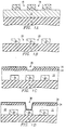
- Figures 1A-1E illustrate a semiconductor structure at several steps in the formation of an interconnection layer.
- a conducting layer 12 which may be of aluminum alloyed with a small amount of copper, with a TiN underlayer and overlayer (not shown) is deposited on an insulating layer 10 (e.g. silicon dioxide or a previous level formed according to the present invention).
- Conducting layer 12 may be connected through insulating layer 10 to an underlying structure (not shown).
- a layer of photoresist 14 is spun on over conducting layer 12, exposed through a mask pattern and developed, such that the photoresist layer 14 contains gaps 16 where conducting layer 12 is to be removed.
- FIG. 1B conducting material has been removed using an etching process which removes material below gaps in the photoresist layer to create patterned conductors 18 separated by gaps 20.
- the photoresist 14 of Figure 1A has also been stripped and does not appear in Figure 1B.
- Figure 1C shows additional layers added to the structure.
- a porous dielectric layer 22 fills the gaps 20 of Figure 1B, as well as covering patterned conductors 18 to a thickness roughly equivalent to the thickness of the conductors themselves (layer 22 generally having a depth measured in gap 20 of at least 150% of conductor thickness and shown as 200% of conductor thickness).
- This porous layer may, for example, be formed by first depositing and gelling a gel precursor solution (some of which are described in detail in the specific chemical examples) in the gaps between and over conductors 18 to form a wet gel sublayer.
- the method of application may be, for example, a spin-on technique in a controlled atmosphere which limits solvent evaporation.
- the precursor may be prepared, for example, by the following 2-step process. First, TEOS stock, a mixture of tetraethylorthosilicate (TEOS), ethanol, water, and HCl, in the approximate molar ratio 1:3:1:0.0007, is prepared by stirring these ingredients under constant reflux at 60 degrees C for 1.5 hours.
- 0.05 M ammonium hydroxide is added to the TEOS stock, 0.1 ml for each ml of TEOS stock.
- the precursor solution may preferably be gelled on the substrate, a process which typically takes from 1 minute to 12 hours, depending on the solution and method of gelling.
- the wet gel can be allowed time to age, generally about a day (although it may be much shorter), at one or more controlled temperatures. Gelation and aging may preferably be accomplished by letting the device sit in a saturated ethanol atmosphere for approximately 24 hours at about 37 degrees C.
- the water may be removed from the wet gel, preferably by immersing the wafer in pure ethanol.
- a surface modification step is performed on the wet gel, replacing a substantial number of the molecules on the pore walls with those of another species.
- Surface modification may be performed, for example, by immersing the wafer in a hexane solution containing about 10% by volume trimethylchlorosilane (TMCS).
- TMCS trimethylchlorosilane
- the final shrinkage may be adjusted from the large shinkage typical of an unmodified xerogel (with uncontrolled shrinkage) to a shrinkage of only a few percent, heretofore only achievable with a supercritical aerogel technique.
- approximately 30% of the reactive surface groups must be replaced to substantially alleviate densification.
- the replacement surface species may be chosen because of its wetting properties in combination with specific pore fluids; the surface modification may result in a pore fluid contact angle closer to 90 degrees, which is desirable because of a corresponding decrease in capillary forces in the gel structure during drying. It is believed that the surface modification prevents surface condensation reactions, and may also reduce capillary pressure by changing pore fluid contact angle, thereby allowing pores in the surface modified gel to better survive drying.
- porous layer 22 is dehydroxylated (hydroxyl groups present on the internal pore surfaces are removed) at this point by baking the device in a forming gas (10 vol % H2, 90 vol % N2), preferably at about 450 C. It has been previously recognized that this process may improve the dielectric properties of the porous structure. It is recognized herein that further advantages of dehydroxylation (which tends to remove other surface species as well) may include improvements in controllability and selectivity of the porous dielectric etch process.
- aprotic solvent e.g. acetone, hexane
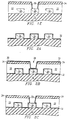
- a cap layer 24 may then be deposited over porous layer 22, preferably by a low temperature dry technique such as PECVD (plasma enhanced chemical vapor deposition) of TEOS to form a silicon dioxide layer, or a plasma silicon nitride deposition process.
- PECVD plasma enhanced chemical vapor deposition
- the PECVD TEOS technique has been used so that several important issues related to the use of similar materials for both cap layer 24 and underlying porous layer 22 may be examined.
- Figure 1C shows a new layer of photoresist 26 deposited over cap layer 24.
- a via 28 is shown after mask patterning and developing of photoresist layer 26, and after anistropic etch of cap layer 24.
- FIG 1C an ideally controlled etch of via 28, which was stopped exactly at the boundary between porous and cap layers, is shown.
- both layers are formed from similar materials, both will probably be similarly affected by the cap layer etch, except that porous layer 22 has a density preferably 1/3 to 1/5 that of the cap layer. This translates to a relative etch rate roughly 3 to 5 times higher for the porous material, such that, for example, a 10% overetch of cap layer 24 may actually result in a 50% overetch into the porous layer.
- materials with a higher selectivity may be chosen, the cap layer may be kept as thin as possible, and planarizing cap layers (which may result in varying cap layer thickness across a wafer) should probably be avoided.
- Figure 1D illustrates the device after photoresist 26 has been stripped and via 28 has been etched through dielectric layer 22 to conductor 18. Such an etch may preferably be carried out using reactive ion etching (RIE) and standard SiO2 etchants for TEOS-based porous dielectrics, with etch rates adjusted appropriately for a given porosity.
- RIE reactive ion etching
- This figure further shows a via passivation layer 30 applied conformally over the exposed surfaces of the device.
- via passivation layer 30 is constructed of a material similar to cap layer 24 (PECVD TEOS deposition of silicon dioxide for this example), although this is not required.
- Figure 1E shows the via passivation layer 30 remaining only on the via sidewalls, after an anisotropic etch has been used to remove passivation material from the bottom of the via and from the top of the hard mask.
- This configuration is desirable because it provides decreased capacitive coupling, while maintaining standard dielectric surface materials such as oxides and nitrides for subsequent via metallization, photolithography, and the like.
- Figures 2A-2C show a second embodiment which includes a substrate encapsulation layer 32 deposited conformally over the patterned conductors 18 and substrate 10.
- Figure 2A shows the structure after patterning of the conductors and deposition of encapsulation layer 32 (e.g. silicon dioxide). Steps similar to those of the first embodiment are then performed to construct the cross-section of Figure 2B.
- This embodiment differs in that the bottom of via 28 is now typically obstructed by both substrate encapsulation layer 32 and via passivation layer 30. Clearing the bottom of the via utilizes an anisotropic etch which can remove both obstructing layers.
- cap layer may be deposited with additional thickness designed to be sacrificial; that is, a portion of the cap layer may be removed during etching of the passivating layers.
- porous dielectric layer 22 may be completely enclosed by the passivating and encapsulating material, such that conducting material is completely isolated from porous dielectric material.
- Figures 3A-3C Another method which may be used with a substrate encapsulation layer is depicted in Figures 3A-3C.
- Figure 3A is identical to Figure 2A, but Figure 3B shows a cap layer 24 covered by a hard mask layer 34 which is formed of a material resistant to the passivation/encapsulation layer etch.
- a hard mask layer 34 which is formed of a material resistant to the passivation/encapsulation layer etch.
- One choice may be a silicon nitride hard mask, if for example, passivating layer 30 and encapsulation layer 32 are constructed of primarily silicon dioxide. This embodiment may require an additional etch step during via opening to remove hard mask layer 34 from the via opening.
- via passivation layer 30 is formed to directly overlay hard mask layer 34 instead of cap layer 24.
- the anisotropic etch to clear the bottom of via 28 now will remove passivation layer 30 from at least the top surfaces of hard mask layer 34.
- the hard mask layer then acts as an etch stop to prevent etching into cap layer 24, although the tops of the passivation layer 30 lining the via sidewalls are not protected from the etch.
- hard mask 34 may be left in place.
- the hard mask may be removed by a selective etch to complete the structure of Figure 3C.
- such a hard mask technique may also be used as a thin etch stop at the bottom of cap layer 24 to prevent the cap layer etch from penetrating deeply into the porous layer.
- Figure 4 shows a cross-section of an embodiment of the invention which illustrates how the various features and advantages of the invention may be employed on multiple layers of patterned conductors.
- An intermediate structure similar to that of Figure 2C is built upon by first adding a second layer of patterned conductors 38 above cap layer 24 and in via 28. This layer may be formed by depositing several sublayers (TiN/AlCu alloy/TiN, for example) of conducting material over the structure and patterning this material in a manner similar to the formation of conductors 18. After patterning of the second conducting layer, a second substrate encapsulation layer 36 is deposited over the exposed surfaces of cap layer 24 and second conductor layer 38, followed by a second porous dielectric layer 40 and a second cap layer 42. If connections to yet another overlying layer of conductors (not shown) is desired, via formation on the second conducting layer may then proceed according to one of the methods of the invention.
- TiN/AlCu alloy/TiN for example
- the invention is not to be construed as limited to the particular examples described herein, as these are to be regarded as illustrative, rather than restrictive.
- the invention is intended to cover all processes and structures which do not depart from the spirit and scope of the invention.
- the invention is primarily directed to integrating a porous dielectric layer into an otherwise standard semiconductor device, and such a layer may be used in many semiconductor device structures other than the specific structures shown herein. Properties of some of the specific examples may be combined without deviating from the nature of the invention.
Landscapes
- Internal Circuitry In Semiconductor Integrated Circuit Devices (AREA)
- Formation Of Insulating Films (AREA)
Applications Claiming Priority (2)
| Application Number | Priority Date | Filing Date | Title |
|---|---|---|---|
| US08/286,761 US5472913A (en) | 1994-08-05 | 1994-08-05 | Method of fabricating porous dielectric material with a passivation layer for electronics applications |
| US286761 | 1994-08-05 |
Publications (1)
| Publication Number | Publication Date |
|---|---|
| EP0703610A1 true EP0703610A1 (de) | 1996-03-27 |
Family
ID=23100054
Family Applications (1)
| Application Number | Title | Priority Date | Filing Date |
|---|---|---|---|
| EP95112382A Withdrawn EP0703610A1 (de) | 1994-08-05 | 1995-08-07 | Verfahren zur Herstellung von Verbindungsstrukturen für ein Halbleiterbauelement, unter Verwendung von Isolierschichten aus porösem dielektrischen Material, und damit hergestellte Strukturen |
Country Status (5)
| Country | Link |
|---|---|
| US (2) | US5472913A (de) |
| EP (1) | EP0703610A1 (de) |
| JP (1) | JPH0864680A (de) |
| KR (1) | KR100382708B1 (de) |
| TW (1) | TW351848B (de) |
Cited By (3)
| Publication number | Priority date | Publication date | Assignee | Title |
|---|---|---|---|---|
| EP0892428A3 (de) * | 1997-07-17 | 1999-11-24 | Sharp Kabushiki Kaisha | Verfahren zum Herstellen von Kontakten mit niedrigem Widerstand zwischen Metallisierungsschichten eines Integrierten Schaltkreises und dadurch hergestellte Strukturen |
| EP1054444A1 (de) * | 1999-05-19 | 2000-11-22 | Applied Materials, Inc. | Abscheidungsverfahren für einen porösen SiO2-Film mit einer niedrigen Dielektrizitätskonstante |
| US6479374B1 (en) | 1998-04-01 | 2002-11-12 | Asahi Kasei Kabushiki Kaisha | Method of manufacturing interconnection structural body |
Families Citing this family (105)
| Publication number | Priority date | Publication date | Assignee | Title |
|---|---|---|---|---|
| JP3158749B2 (ja) * | 1992-12-16 | 2001-04-23 | ヤマハ株式会社 | 半導体装置 |
| US6278174B1 (en) * | 1994-04-28 | 2001-08-21 | Texas Instruments Incorporated | Integrated circuit insulator and structure using low dielectric insulator material including HSQ and fluorinated oxide |
| US5461003A (en) * | 1994-05-27 | 1995-10-24 | Texas Instruments Incorporated | Multilevel interconnect structure with air gaps formed between metal leads |
| US5504042A (en) * | 1994-06-23 | 1996-04-02 | Texas Instruments Incorporated | Porous dielectric material with improved pore surface properties for electronics applications |
| JPH11307633A (ja) * | 1997-11-17 | 1999-11-05 | Sony Corp | 低誘電率膜を有する半導体装置、およびその製造方法 |
| US6744091B1 (en) * | 1995-01-31 | 2004-06-01 | Fujitsu Limited | Semiconductor storage device with self-aligned opening and method for fabricating the same |
| US5627082A (en) * | 1995-03-29 | 1997-05-06 | Texas Instruments Incorporated | High thermal resistance backfill material for hybrid UFPA's |
| US5638599A (en) * | 1995-03-29 | 1997-06-17 | Texas Instruments Incorporated | Method of fabricating hybrid uncooled infrared detectors |
| JP2845176B2 (ja) * | 1995-08-10 | 1999-01-13 | 日本電気株式会社 | 半導体装置 |
| US6380105B1 (en) | 1996-11-14 | 2002-04-30 | Texas Instruments Incorporated | Low volatility solvent-based method for forming thin film nanoporous aerogels on semiconductor substrates |
| US6130152A (en) | 1995-11-16 | 2000-10-10 | Texas Instruments Incorporated | Aerogel thin film formation from multi-solvent systems |
| US6319852B1 (en) | 1995-11-16 | 2001-11-20 | Texas Instruments Incorporated | Nanoporous dielectric thin film formation using a post-deposition catalyst |
| US5736425A (en) * | 1995-11-16 | 1998-04-07 | Texas Instruments Incorporated | Glycol-based method for forming a thin-film nanoporous dielectric |
| US6063714A (en) * | 1995-11-16 | 2000-05-16 | Texas Instruments Incorporated | Nanoporous dielectric thin film surface modification |
| US6037277A (en) * | 1995-11-16 | 2000-03-14 | Texas Instruments Incorporated | Limited-volume apparatus and method for forming thin film aerogels on semiconductor substrates |
| US5807607A (en) * | 1995-11-16 | 1998-09-15 | Texas Instruments Incorporated | Polyol-based method for forming thin film aerogels on semiconductor substrates |
| US5753305A (en) * | 1995-11-16 | 1998-05-19 | Texas Instruments Incorporated | Rapid aging technique for aerogel thin films |
| US5683930A (en) * | 1995-12-06 | 1997-11-04 | Micron Technology Inc. | SRAM cell employing substantially vertically elongated pull-up resistors and methods of making, and resistor constructions and methods of making |
| KR100198678B1 (ko) * | 1996-02-28 | 1999-06-15 | 구본준 | 금속 배선 구조 및 형성방법 |
| JPH09260492A (ja) * | 1996-03-25 | 1997-10-03 | Toshiba Corp | 半導体装置の製造方法 |
| US5886410A (en) * | 1996-06-26 | 1999-03-23 | Intel Corporation | Interconnect structure with hard mask and low dielectric constant materials |
| JP3941133B2 (ja) * | 1996-07-18 | 2007-07-04 | 富士通株式会社 | 半導体装置およびその製造方法 |
| KR100192589B1 (ko) * | 1996-08-08 | 1999-06-15 | 윤종용 | 반도체 장치 및 그 제조방법 |
| US5849644A (en) * | 1996-08-13 | 1998-12-15 | Micron Technology, Inc. | Semiconductor processing methods of chemical vapor depositing SiO2 on a substrate |
| US20010012700A1 (en) * | 1998-12-15 | 2001-08-09 | Klaus F. Schuegraf | Semiconductor processing methods of chemical vapor depositing sio2 on a substrate |
| CA2213034C (en) * | 1996-09-02 | 2002-12-17 | Murata Manufacturing Co., Ltd. | A semiconductor device with a passivation film |
| JP3305211B2 (ja) * | 1996-09-10 | 2002-07-22 | 松下電器産業株式会社 | 半導体装置及びその製造方法 |
| JPH10135270A (ja) * | 1996-10-31 | 1998-05-22 | Casio Comput Co Ltd | 半導体装置及びその製造方法 |
| US5922299A (en) | 1996-11-26 | 1999-07-13 | Battelle Memorial Institute | Mesoporous-silica films, fibers, and powders by evaporation |
| US5849367A (en) * | 1996-12-11 | 1998-12-15 | Texas Instruments Incorporated | Elemental titanium-free liner and fabrication process for inter-metal connections |
| US6255156B1 (en) | 1997-02-07 | 2001-07-03 | Micron Technology, Inc. | Method for forming porous silicon dioxide insulators and related structures |
| EP0875905B1 (de) * | 1997-04-28 | 2001-06-27 | STMicroelectronics S.r.l. | Verbundfolie mit niedriger Dielektrizitätskonstante für integrierte Schaltungen aus anorganischem Aerogel und mit einem organischen Füllstoff gepfropftes anorganisches Material sowie dessen Herstellung |
| JP4663038B2 (ja) * | 1997-05-28 | 2011-03-30 | 三菱電機株式会社 | コンタクトホールの形成方法 |
| US6448331B1 (en) | 1997-07-15 | 2002-09-10 | Asahi Kasei Kabushiki Kaisha | Alkoxysilane/organic polymer composition for thin insulating film production and use thereof |
| US6048803A (en) * | 1997-08-19 | 2000-04-11 | Advanced Microdevices, Inc. | Method of fabricating a semiconductor device having fluorine bearing oxide between conductive lines |
| US6294455B1 (en) | 1997-08-20 | 2001-09-25 | Micron Technology, Inc. | Conductive lines, coaxial lines, integrated circuitry, and methods of forming conductive lines, coaxial lines, and integrated circuitry |
| US6187677B1 (en) | 1997-08-22 | 2001-02-13 | Micron Technology, Inc. | Integrated circuitry and methods of forming integrated circuitry |
| US6143616A (en) | 1997-08-22 | 2000-11-07 | Micron Technology, Inc. | Methods of forming coaxial integrated circuitry interconnect lines |
| US6143640A (en) * | 1997-09-23 | 2000-11-07 | International Business Machines Corporation | Method of fabricating a stacked via in copper/polyimide beol |
| US6236101B1 (en) * | 1997-11-05 | 2001-05-22 | Texas Instruments Incorporated | Metallization outside protective overcoat for improved capacitors and inductors |
| US6248168B1 (en) * | 1997-12-15 | 2001-06-19 | Tokyo Electron Limited | Spin coating apparatus including aging unit and solvent replacement unit |
| SG74672A1 (en) * | 1997-12-29 | 2000-08-22 | Texas Instruments Inc | Integrated circuit and method of using porous silicon to achieve component isolation in radio frequency applications |
| JP2921759B1 (ja) | 1998-03-31 | 1999-07-19 | 株式会社半導体理工学研究センター | 半導体装置の製造方法 |
| US5986344A (en) | 1998-04-14 | 1999-11-16 | Advanced Micro Devices, Inc. | Anti-reflective coating layer for semiconductor device |
| JP3114864B2 (ja) * | 1998-04-16 | 2000-12-04 | 日本電気株式会社 | 半導体基板における微細コンタクトおよびその形成方法 |
| US6019906A (en) * | 1998-05-29 | 2000-02-01 | Taiwan Semiconductor Manufacturing Company | Hard masking method for forming patterned oxygen containing plasma etchable layer |
| US6121098A (en) * | 1998-06-30 | 2000-09-19 | Infineon Technologies North America Corporation | Semiconductor manufacturing method |
| JP2000031274A (ja) * | 1998-07-14 | 2000-01-28 | Matsushita Electric Ind Co Ltd | 半導体装置 |
| US6140221A (en) * | 1998-07-29 | 2000-10-31 | Philips Electronics North America Corp. | Method for forming vias through porous dielectric material and devices formed thereby |
| US6235630B1 (en) | 1998-08-19 | 2001-05-22 | Micron Technology, Inc. | Silicide pattern structures and methods of fabricating the same |
| US6133619A (en) * | 1998-08-31 | 2000-10-17 | Advanced Micro Devices, Inc. | Reduction of silicon oxynitride film delamination in integrated circuit inter-level dielectrics |
| US6124640A (en) * | 1998-08-31 | 2000-09-26 | Advanced Micro Devices, Inc. | Scalable and reliable integrated circuit inter-level dielectric |
| US6187672B1 (en) * | 1998-09-22 | 2001-02-13 | Conexant Systems, Inc. | Interconnect with low dielectric constant insulators for semiconductor integrated circuit manufacturing |
| US6153528A (en) * | 1998-10-14 | 2000-11-28 | United Silicon Incorporated | Method of fabricating a dual damascene structure |
| TW429576B (en) * | 1998-10-14 | 2001-04-11 | United Microelectronics Corp | Manufacturing method for metal interconnect |
| US6090674A (en) * | 1998-11-09 | 2000-07-18 | Taiwan Semiconductor Manufacturing Company | Method of forming a hole in the sub quarter micron range |
| US6281115B1 (en) * | 1998-11-16 | 2001-08-28 | Industrial Technology Research Institute | Sidewall protection for a via hole formed in a photosensitive, low dielectric constant layer |
| US6444564B1 (en) | 1998-11-23 | 2002-09-03 | Advanced Micro Devices, Inc. | Method and product for improved use of low k dielectric material among integrated circuit interconnect structures |
| US6383466B1 (en) | 1998-12-28 | 2002-05-07 | Battelle Memorial Institute | Method of dehydroxylating a hydroxylated material and method of making a mesoporous film |
| US6329017B1 (en) | 1998-12-23 | 2001-12-11 | Battelle Memorial Institute | Mesoporous silica film from a solution containing a surfactant and methods of making same |
| US6159842A (en) * | 1999-01-11 | 2000-12-12 | Taiwan Semiconductor Manufacturing Company | Method for fabricating a hybrid low-dielectric-constant intermetal dielectric (IMD) layer with improved reliability for multilevel interconnections |
| US6165905A (en) * | 1999-01-20 | 2000-12-26 | Philips Electronics, North America Corp. | Methods for making reliable via structures having hydrophobic inner wall surfaces |
| US6770572B1 (en) * | 1999-01-26 | 2004-08-03 | Alliedsignal Inc. | Use of multifunctional si-based oligomer/polymer for the surface modification of nanoporous silica films |
| JP3084367B1 (ja) * | 1999-03-17 | 2000-09-04 | キヤノン販売株式会社 | 層間絶縁膜の形成方法及び半導体装置 |
| US6287987B1 (en) | 1999-04-30 | 2001-09-11 | Lsi Logic Corporation | Method and apparatus for deposition of porous silica dielectrics |
| US6329280B1 (en) | 1999-05-13 | 2001-12-11 | International Business Machines Corporation | Interim oxidation of silsesquioxane dielectric for dual damascene process |
| US6312793B1 (en) * | 1999-05-26 | 2001-11-06 | International Business Machines Corporation | Multiphase low dielectric constant material |
| US6452275B1 (en) * | 1999-06-09 | 2002-09-17 | Alliedsignal Inc. | Fabrication of integrated circuits with borderless vias |
| US6221780B1 (en) | 1999-09-29 | 2001-04-24 | International Business Machines Corporation | Dual damascene flowable oxide insulation structure and metallic barrier |
| US20040089238A1 (en) * | 1999-10-04 | 2004-05-13 | Jerome Birnbaum | Vacuum/gas phase reactor for dehydroxylation and alkylation of porous silica |
| US6348736B1 (en) | 1999-10-29 | 2002-02-19 | International Business Machines Corporation | In situ formation of protective layer on silsesquioxane dielectric for dual damascene process |
| US6180518B1 (en) * | 1999-10-29 | 2001-01-30 | Lucent Technologies Inc. | Method for forming vias in a low dielectric constant material |
| US20010051420A1 (en) * | 2000-01-19 | 2001-12-13 | Besser Paul R. | Dielectric formation to seal porosity of low dielectic constant (low k) materials after etch |
| JP3365554B2 (ja) * | 2000-02-07 | 2003-01-14 | キヤノン販売株式会社 | 半導体装置の製造方法 |
| US6420193B1 (en) * | 2000-03-17 | 2002-07-16 | Advance Micro Devices, Inc. | Repair of film having an SI-O backbone |
| US6720249B1 (en) * | 2000-04-17 | 2004-04-13 | International Business Machines Corporation | Protective hardmask for producing interconnect structures |
| DE10036725C2 (de) | 2000-07-27 | 2002-11-28 | Infineon Technologies Ag | Verfahren zur Herstellung einer porösen Isolierschicht mit niedriger Dielektrizitätskonstante auf einem Halbleitersubstrat |
| US6753270B1 (en) | 2000-08-04 | 2004-06-22 | Applied Materials Inc. | Process for depositing a porous, low dielectric constant silicon oxide film |
| US6617239B1 (en) | 2000-08-31 | 2003-09-09 | Micron Technology, Inc. | Subtractive metallization structure and method of making |
| US6787906B1 (en) * | 2000-10-30 | 2004-09-07 | Samsung Electronics Co., Ltd. | Bit line pad and borderless contact on bit line stud with localized etch stop layer formed in an undermined region |
| US6383920B1 (en) | 2001-01-10 | 2002-05-07 | International Business Machines Corporation | Process of enclosing via for improved reliability in dual damascene interconnects |
| US6555909B1 (en) * | 2001-01-11 | 2003-04-29 | Advanced Micro Devices, Inc. | Seedless barrier layers in integrated circuits and a method of manufacture therefor |
| FR2819635B1 (fr) * | 2001-01-18 | 2004-01-23 | St Microelectronics Sa | Procede de fabrication de reseaux d'interconnexions |
| US6537908B2 (en) * | 2001-02-28 | 2003-03-25 | International Business Machines Corporation | Method for dual-damascence patterning of low-k interconnects using spin-on distributed hardmask |
| US6603204B2 (en) * | 2001-02-28 | 2003-08-05 | International Business Machines Corporation | Low-k interconnect structure comprised of a multilayer of spin-on porous dielectrics |
| WO2002071476A2 (en) * | 2001-03-06 | 2002-09-12 | Advanced Micro Devices, Inc. | Method of forming conductive interconnections in porous insulating films and associated device |
| US20020177303A1 (en) * | 2001-05-23 | 2002-11-28 | Qing-Tang Jiang | Method for sealing via sidewalls in porous low-k dielectric layers |
| US6602780B2 (en) * | 2001-09-06 | 2003-08-05 | Taiwan Semiconductor Manufacturing Co., Ltd | Method for protecting sidewalls of etched openings to prevent via poisoning |
| WO2003044843A2 (en) * | 2001-11-16 | 2003-05-30 | Trikon Holdings Limited | Forming low k dielectric layers |
| JP2005512298A (ja) * | 2001-12-10 | 2005-04-28 | コーニンクレッカ フィリップス エレクトロニクス エヌ ヴィ | Elディスプレイ装置及び該装置の製造方法 |
| US20030218253A1 (en) * | 2001-12-13 | 2003-11-27 | Avanzino Steven C. | Process for formation of a wiring network using a porous interlevel dielectric and related structures |
| US7226853B2 (en) * | 2001-12-26 | 2007-06-05 | Applied Materials, Inc. | Method of forming a dual damascene structure utilizing a three layer hard mask structure |
| US6806203B2 (en) | 2002-03-18 | 2004-10-19 | Applied Materials Inc. | Method of forming a dual damascene structure using an amorphous silicon hard mask |
| JP3596616B2 (ja) * | 2002-09-25 | 2004-12-02 | 沖電気工業株式会社 | 半導体装置の製造方法 |
| JP2004296476A (ja) * | 2003-03-25 | 2004-10-21 | Semiconductor Leading Edge Technologies Inc | 半導体装置の製造方法 |
| US6921978B2 (en) * | 2003-05-08 | 2005-07-26 | International Business Machines Corporation | Method to generate porous organic dielectric |
| US8263983B2 (en) | 2003-10-28 | 2012-09-11 | Semiconductor Energy Laboratory Co., Ltd. | Wiring substrate and semiconductor device |
| JP4094574B2 (ja) * | 2004-03-08 | 2008-06-04 | シャープ株式会社 | 半導体装置及びその製造方法 |
| KR100835435B1 (ko) | 2006-11-28 | 2008-06-04 | 동부일렉트로닉스 주식회사 | 반도체 소자의 패시베이션 형성방법 |
| JP4389962B2 (ja) * | 2007-04-26 | 2009-12-24 | ソニー株式会社 | 半導体装置、電子機器、および半導体装置の製造方法 |
| US8053861B2 (en) * | 2009-01-26 | 2011-11-08 | Novellus Systems, Inc. | Diffusion barrier layers |
| FR3000602B1 (fr) * | 2012-12-28 | 2016-06-24 | Commissariat A L Energie Atomique Et Aux Energies Alternatives | Procede de gravure d'un materiau dielectrique poreux |
| US10134634B2 (en) * | 2014-11-04 | 2018-11-20 | Georgia Tech Research Corporation | Metal-assisted chemical etching of a semiconductive substrate with high aspect ratio, high geometic uniformity, and controlled 3D profiles |
| CN112151497B (zh) * | 2019-06-28 | 2023-08-22 | 台湾积体电路制造股份有限公司 | 半导体结构以及形成半导体结构的方法 |
| DE102019131408B4 (de) | 2019-06-28 | 2025-12-04 | Taiwan Semiconductor Manufacturing Company, Ltd. | Verbesserte Kontaktierung von Metallleitungen bei Fehlausrichtung von BEOL-Durchkontaktierungen |
Citations (7)
| Publication number | Priority date | Publication date | Assignee | Title |
|---|---|---|---|---|
| EP0177845A1 (de) * | 1984-09-28 | 1986-04-16 | Siemens Aktiengesellschaft | Integrierter Schaltkreis mit Mehrlagenverdrahtung und Verfahren zu seiner Herstellung |
| JPS61268043A (ja) * | 1985-05-23 | 1986-11-27 | Nippon Telegr & Teleph Corp <Ntt> | 半導体装置の製造方法 |
| JPS63208248A (ja) * | 1987-02-24 | 1988-08-29 | Nec Corp | 半導体装置 |
| US5103288A (en) | 1988-03-15 | 1992-04-07 | Nec Corporation | Semiconductor device having multilayered wiring structure with a small parasitic capacitance |
| GB2266181A (en) * | 1992-03-31 | 1993-10-20 | Mitsubishi Electric Corp | Semiconductor integrated circuit with an insulating layer incorporating vacancies |
| EP0571108A1 (de) * | 1992-05-06 | 1993-11-24 | STMicroelectronics, Inc. | Kontaktlöcherstruktur für eine Halbleiter-Schaltung und Herstellungsverfahren |
| US5284801A (en) * | 1992-07-22 | 1994-02-08 | Vlsi Technology, Inc. | Methods of moisture protection in semiconductor devices utilizing polyimides for inter-metal dielectric |
Family Cites Families (18)
| Publication number | Priority date | Publication date | Assignee | Title |
|---|---|---|---|---|
| JPS5731144A (en) * | 1980-07-31 | 1982-02-19 | Fujitsu Ltd | Mamufacture of semiconductor device |
| FR2526225B1 (fr) * | 1982-04-30 | 1985-11-08 | Radiotechnique Compelec | Procede de realisation d'un condensateur integre, et dispositif ainsi obtenu |
| US4652467A (en) * | 1985-02-25 | 1987-03-24 | The United States Of America As Represented By The United States Department Of Energy | Inorganic-polymer-derived dielectric films |
| JPH0715938B2 (ja) * | 1985-05-23 | 1995-02-22 | 日本電信電話株式会社 | 半導体装置およびその製造方法 |
| US4876217A (en) * | 1988-03-24 | 1989-10-24 | Motorola Inc. | Method of forming semiconductor structure isolation regions |
| US4987101A (en) * | 1988-12-16 | 1991-01-22 | International Business Machines Corporation | Method for providing improved insulation in VLSI and ULSI circuits |
| JP2556146B2 (ja) * | 1989-09-19 | 1996-11-20 | 日本電気株式会社 | 多層配線 |
| JPH04174541A (ja) * | 1990-03-28 | 1992-06-22 | Nec Corp | 半導体集積回路及びその製造方法 |
| CA2017720C (en) * | 1990-05-29 | 1999-01-19 | Luc Ouellet | Sog with moisture-resistant protective capping layer |
| JPH04311059A (ja) * | 1991-04-09 | 1992-11-02 | Oki Electric Ind Co Ltd | 配線容量の低減方法 |
| US5300813A (en) * | 1992-02-26 | 1994-04-05 | International Business Machines Corporation | Refractory metal capped low resistivity metal conductor lines and vias |
| US5342808A (en) * | 1992-03-12 | 1994-08-30 | Hewlett-Packard Company | Aperture size control for etched vias and metal contacts |
| US5302551A (en) * | 1992-05-11 | 1994-04-12 | National Semiconductor Corporation | Method for planarizing the surface of an integrated circuit over a metal interconnect layer |
| US5393712A (en) * | 1993-06-28 | 1995-02-28 | Lsi Logic Corporation | Process for forming low dielectric constant insulation layer on integrated circuit structure |
| US5488015A (en) * | 1994-05-20 | 1996-01-30 | Texas Instruments Incorporated | Method of making an interconnect structure with an integrated low density dielectric |
| US5470802A (en) * | 1994-05-20 | 1995-11-28 | Texas Instruments Incorporated | Method of making a semiconductor device using a low dielectric constant material |
| US5494858A (en) * | 1994-06-07 | 1996-02-27 | Texas Instruments Incorporated | Method for forming porous composites as a low dielectric constant layer with varying porosity distribution electronics applications |
| US5504042A (en) * | 1994-06-23 | 1996-04-02 | Texas Instruments Incorporated | Porous dielectric material with improved pore surface properties for electronics applications |
-
1994
- 1994-08-05 US US08/286,761 patent/US5472913A/en not_active Expired - Lifetime
-
1995
- 1995-06-07 US US08/476,164 patent/US5661344A/en not_active Expired - Lifetime
- 1995-08-04 KR KR1019950024039A patent/KR100382708B1/ko not_active Expired - Lifetime
- 1995-08-04 JP JP7199967A patent/JPH0864680A/ja active Pending
- 1995-08-07 EP EP95112382A patent/EP0703610A1/de not_active Withdrawn
- 1995-09-06 TW TW084109296A patent/TW351848B/zh not_active IP Right Cessation
Patent Citations (7)
| Publication number | Priority date | Publication date | Assignee | Title |
|---|---|---|---|---|
| EP0177845A1 (de) * | 1984-09-28 | 1986-04-16 | Siemens Aktiengesellschaft | Integrierter Schaltkreis mit Mehrlagenverdrahtung und Verfahren zu seiner Herstellung |
| JPS61268043A (ja) * | 1985-05-23 | 1986-11-27 | Nippon Telegr & Teleph Corp <Ntt> | 半導体装置の製造方法 |
| JPS63208248A (ja) * | 1987-02-24 | 1988-08-29 | Nec Corp | 半導体装置 |
| US5103288A (en) | 1988-03-15 | 1992-04-07 | Nec Corporation | Semiconductor device having multilayered wiring structure with a small parasitic capacitance |
| GB2266181A (en) * | 1992-03-31 | 1993-10-20 | Mitsubishi Electric Corp | Semiconductor integrated circuit with an insulating layer incorporating vacancies |
| EP0571108A1 (de) * | 1992-05-06 | 1993-11-24 | STMicroelectronics, Inc. | Kontaktlöcherstruktur für eine Halbleiter-Schaltung und Herstellungsverfahren |
| US5284801A (en) * | 1992-07-22 | 1994-02-08 | Vlsi Technology, Inc. | Methods of moisture protection in semiconductor devices utilizing polyimides for inter-metal dielectric |
Non-Patent Citations (2)
| Title |
|---|
| PATENT ABSTRACTS OF JAPAN vol. 011, no. 122 (E - 500) 16 April 1987 (1987-04-16) * |
| PATENT ABSTRACTS OF JAPAN vol. 012, no. 498 (E - 698) 24 December 1988 (1988-12-24) * |
Cited By (3)
| Publication number | Priority date | Publication date | Assignee | Title |
|---|---|---|---|---|
| EP0892428A3 (de) * | 1997-07-17 | 1999-11-24 | Sharp Kabushiki Kaisha | Verfahren zum Herstellen von Kontakten mit niedrigem Widerstand zwischen Metallisierungsschichten eines Integrierten Schaltkreises und dadurch hergestellte Strukturen |
| US6479374B1 (en) | 1998-04-01 | 2002-11-12 | Asahi Kasei Kabushiki Kaisha | Method of manufacturing interconnection structural body |
| EP1054444A1 (de) * | 1999-05-19 | 2000-11-22 | Applied Materials, Inc. | Abscheidungsverfahren für einen porösen SiO2-Film mit einer niedrigen Dielektrizitätskonstante |
Also Published As
| Publication number | Publication date |
|---|---|
| US5661344A (en) | 1997-08-26 |
| JPH0864680A (ja) | 1996-03-08 |
| US5472913A (en) | 1995-12-05 |
| TW351848B (en) | 1999-02-01 |
| KR100382708B1 (ko) | 2003-07-07 |
Similar Documents
| Publication | Publication Date | Title |
|---|---|---|
| US5472913A (en) | Method of fabricating porous dielectric material with a passivation layer for electronics applications | |
| US5488015A (en) | Method of making an interconnect structure with an integrated low density dielectric | |
| US5789819A (en) | Low dielectric constant material for electronics applications | |
| EP0687004B1 (de) | Poröses Dielektrikum auf Halbleiterbauelementen und Verfahren zur dessen Herstellung | |
| US5668398A (en) | Multilevel interconnect structure with air gaps formed between metal leads | |
| US5750415A (en) | Low dielectric constant layers via immiscible sol-gel processing | |
| US5891804A (en) | Process for conductors with selective deposition | |
| US5708559A (en) | Precision analog metal-metal capacitor | |
| US5565384A (en) | Self-aligned via using low permittivity dielectric | |
| EP0680085A1 (de) | Herstellung von Löchern in polymerischen Materialien | |
| JPH10189733A (ja) | 多孔性誘電体の金属被覆法 | |
| US5960316A (en) | Method to fabricate unlanded vias with a low dielectric constant material as an intraline dielectric | |
| US5880030A (en) | Unlanded via structure and method for making same | |
| GB2325083A (en) | A dual damascene process | |
| JP3526289B2 (ja) | 半導体装置の製造方法 | |
| US6303465B1 (en) | Method of forming low leakage current borderless contact | |
| US6133628A (en) | Metal layer interconnects with improved performance characteristics | |
| KR100684905B1 (ko) | 다마신 공정의 방법 | |
| JP2003060034A (ja) | 半導体装置及びその製造方法 | |
| US20030119294A1 (en) | Method for forming wiring in semiconductor device | |
| KR980011890A (ko) | 반도체 장치의 콘택홀 매립 방법 | |
| JP2002050688A (ja) | 半導体装置およびその製造方法 | |
| JPH10303193A (ja) | 選択的沈着を用いた導電体の処理工程 | |
| KR20030059467A (ko) | 반도체 소자의 제조방법 |
Legal Events
| Date | Code | Title | Description |
|---|---|---|---|
| PUAI | Public reference made under article 153(3) epc to a published international application that has entered the european phase |
Free format text: ORIGINAL CODE: 0009012 |
|
| AK | Designated contracting states |
Kind code of ref document: A1 Designated state(s): DE FR GB IT NL |
|
| 17P | Request for examination filed |
Effective date: 19961211 |
|
| STAA | Information on the status of an ep patent application or granted ep patent |
Free format text: STATUS: THE APPLICATION IS DEEMED TO BE WITHDRAWN |
|
| 18D | Application deemed to be withdrawn |
Effective date: 20060926 |