EP0685892A2 - Verfahren zum Herstellen einer lichtemittierenden Diode - Google Patents
Verfahren zum Herstellen einer lichtemittierenden Diode Download PDFInfo
- Publication number
- EP0685892A2 EP0685892A2 EP95303696A EP95303696A EP0685892A2 EP 0685892 A2 EP0685892 A2 EP 0685892A2 EP 95303696 A EP95303696 A EP 95303696A EP 95303696 A EP95303696 A EP 95303696A EP 0685892 A2 EP0685892 A2 EP 0685892A2
- Authority
- EP
- European Patent Office
- Prior art keywords
- layer
- type gap
- type
- gap
- melted
- Prior art date
- Legal status (The legal status is an assumption and is not a legal conclusion. Google has not performed a legal analysis and makes no representation as to the accuracy of the status listed.)
- Granted
Links
- 238000004519 manufacturing process Methods 0.000 title claims abstract description 13
- 239000000758 substrate Substances 0.000 claims abstract description 25
- IJGRMHOSHXDMSA-UHFFFAOYSA-N Atomic nitrogen Chemical compound N#N IJGRMHOSHXDMSA-UHFFFAOYSA-N 0.000 claims abstract description 8
- 239000007789 gas Substances 0.000 claims abstract description 8
- 229910052757 nitrogen Inorganic materials 0.000 claims abstract description 4
- 239000002019 doping agent Substances 0.000 claims description 13
- 239000007791 liquid phase Substances 0.000 claims description 13
- 239000000463 material Substances 0.000 claims description 4
- OKTJSMMVPCPJKN-UHFFFAOYSA-N Carbon Chemical compound [C] OKTJSMMVPCPJKN-UHFFFAOYSA-N 0.000 claims description 3
- 229910052799 carbon Inorganic materials 0.000 claims description 3
- 238000000034 method Methods 0.000 description 13
- 239000013078 crystal Substances 0.000 description 11
- 238000002513 implantation Methods 0.000 description 6
- 238000001816 cooling Methods 0.000 description 5
- 230000007547 defect Effects 0.000 description 5
- 238000010586 diagram Methods 0.000 description 5
- 238000007796 conventional method Methods 0.000 description 4
- 230000007423 decrease Effects 0.000 description 4
- 230000003247 decreasing effect Effects 0.000 description 4
- 239000007788 liquid Substances 0.000 description 4
- 240000007817 Olea europaea Species 0.000 description 3
- 229910052581 Si3N4 Inorganic materials 0.000 description 2
- 239000012535 impurity Substances 0.000 description 2
- 229920006395 saturated elastomer Polymers 0.000 description 2
- OAICVXFJPJFONN-UHFFFAOYSA-N Phosphorus Chemical compound [P] OAICVXFJPJFONN-UHFFFAOYSA-N 0.000 description 1
- 239000000969 carrier Substances 0.000 description 1
- 230000007812 deficiency Effects 0.000 description 1
- PCHJSUWPFVWCPO-UHFFFAOYSA-N gold Chemical compound [Au] PCHJSUWPFVWCPO-UHFFFAOYSA-N 0.000 description 1
- 239000010931 gold Substances 0.000 description 1
- 229910052737 gold Inorganic materials 0.000 description 1
- 238000002844 melting Methods 0.000 description 1
- 230000008018 melting Effects 0.000 description 1
- 239000013081 microcrystal Substances 0.000 description 1
- 238000012986 modification Methods 0.000 description 1
- 230000004048 modification Effects 0.000 description 1
- 229910052698 phosphorus Inorganic materials 0.000 description 1
- 239000011574 phosphorus Substances 0.000 description 1
- 230000001105 regulatory effect Effects 0.000 description 1
- 239000004065 semiconductor Substances 0.000 description 1
- 229910052717 sulfur Inorganic materials 0.000 description 1
- 230000007704 transition Effects 0.000 description 1
Images



Classifications
-
- H—ELECTRICITY
- H10—SEMICONDUCTOR DEVICES; ELECTRIC SOLID-STATE DEVICES NOT OTHERWISE PROVIDED FOR
- H10H—INORGANIC LIGHT-EMITTING SEMICONDUCTOR DEVICES HAVING POTENTIAL BARRIERS
- H10H20/00—Individual inorganic light-emitting semiconductor devices having potential barriers, e.g. light-emitting diodes [LED]
- H10H20/01—Manufacture or treatment
- H10H20/011—Manufacture or treatment of bodies, e.g. forming semiconductor layers
- H10H20/013—Manufacture or treatment of bodies, e.g. forming semiconductor layers having light-emitting regions comprising only Group III-V materials
-
- H—ELECTRICITY
- H10—SEMICONDUCTOR DEVICES; ELECTRIC SOLID-STATE DEVICES NOT OTHERWISE PROVIDED FOR
- H10H—INORGANIC LIGHT-EMITTING SEMICONDUCTOR DEVICES HAVING POTENTIAL BARRIERS
- H10H20/00—Individual inorganic light-emitting semiconductor devices having potential barriers, e.g. light-emitting diodes [LED]
- H10H20/80—Constructional details
- H10H20/81—Bodies
- H10H20/822—Materials of the light-emitting regions
- H10H20/824—Materials of the light-emitting regions comprising only Group III-V materials, e.g. GaP
- H10H20/8242—Materials of the light-emitting regions comprising only Group III-V materials, e.g. GaP characterised by the dopants
Definitions
- GaP olive color LEDs have a low light-emitting efficiency because GaP crystal is an indirect transition type semiconductor. However, such diodes can emit light with a satisfactory efficiency by introducing nitrogen (N) into the GaP crystal.
- N nitrogen
- GaP containing N is used for a conventional high-intensity GaP olive color LED. In the following description, GaP containing N will be referred to as GaP:N.
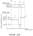
- Figure 5A is a diagram schematically showing epitaxial growth layers of a GaP:N light-emitting diode;
- Figure 5B is a carrier concentration profile of each layer thereof.
- the melted Ga is cooled down to 920°C (hereinafter, referred to as a cooling temperature 1) at 0. 5°C/min.
- a cooling temperature 1 920°C
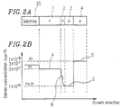
- the melted Ga having an oversaturation degree ⁇ T of 10°C is in contact with the n-type GaP substrate 20 .
- An n-type GaP layer 1 is formed on the n-type GaP substrate 20 by epitaxial growth ( A of Figure 2B ).
- the oversaturation degree ⁇ T of 10°C used is set so as to optimize the light-emitting lifetime of the LED eventually obtained using the melted Ga of the present invention.
- Figure 3 is a graph showing the relationship between the oversaturation degree of the melted Ga used for liquid epitaxial growth and the light-emitting lifetime.
- the light-emitting lifetime is varied depending upon the oversaturation degree of the melted Ga. This is considered as follows: As the oversaturation degree ⁇ T gets higher, an initial epitaxial growth speed becomes faster; therefore, the crystallinity of GaP is improved. However, when the oversaturation degree becomes too high, the microcrystal starts segregating in the melted Ga, which degrades the crystallinity of GaP.
- the oversaturation degree ⁇ T is preferably about 15°C, and more preferably in the range of about 5°C to about 10°C.
- the n-type GaP:N layer 2 with increased N concentration n T and decreased n-type carrier concentration n D ( B of Figure 2B ) can be obtained.
- the thickness of the n-type GaP:N layer 2 is, for example, in the range of about 2 ⁇ m to about 4 ⁇ m.
- the resultant p-type GaP:N layer 3 has a thickness of about 20 ⁇ m and a carrier concentration of about 1016 cm ⁇ 3 or less. During this step, the carrier concentration of the p-type GaP:N layer 3 can be regulated so as to be almost equal to that of the n-type GaP:N layer 2 .
- the n-type GaP layer is formed on the n-type GaP substrate by epitaxial growth by bringing the oversaturated melted Ga into contact with the n-type GaP substrate.
- the n-type GaP:N layer with decreased n-type carrier concentration is formed on the n-type GaP layer by epitaxial growth by bringing the melted Ga into contact with NH3 gas.
- the p-type GaP:N layer having a carrier concentration almost equal to that of a low carrier concentration area of the n-type GaP:N layer is formed on the n-type GaP:N layer by epitaxial growth.
Landscapes
- Led Devices (AREA)
- Liquid Deposition Of Substances Of Which Semiconductor Devices Are Composed (AREA)
Applications Claiming Priority (3)
| Application Number | Priority Date | Filing Date | Title |
|---|---|---|---|
| JP117999/94 | 1994-05-31 | ||
| JP11799994A JP3163217B2 (ja) | 1994-05-31 | 1994-05-31 | 発光ダイオード及びその製造方法 |
| JP11799994 | 1994-05-31 |
Publications (3)
| Publication Number | Publication Date |
|---|---|
| EP0685892A2 true EP0685892A2 (de) | 1995-12-06 |
| EP0685892A3 EP0685892A3 (de) | 1998-04-01 |
| EP0685892B1 EP0685892B1 (de) | 2002-02-06 |
Family
ID=14725545
Family Applications (1)
| Application Number | Title | Priority Date | Filing Date |
|---|---|---|---|
| EP95303696A Expired - Lifetime EP0685892B1 (de) | 1994-05-31 | 1995-05-31 | Verfahren zum Herstellen einer lichtemittierenden Diode |
Country Status (6)
| Country | Link |
|---|---|
| US (1) | US5529938A (de) |
| EP (1) | EP0685892B1 (de) |
| JP (1) | JP3163217B2 (de) |
| KR (1) | KR950034869A (de) |
| DE (1) | DE69525283T2 (de) |
| TW (1) | TW270241B (de) |
Cited By (3)
| Publication number | Priority date | Publication date | Assignee | Title |
|---|---|---|---|---|
| GB2331307A (en) * | 1997-11-15 | 1999-05-19 | Sharp Kk | Growth of buffer layer by molecular beam epitaxy |
| WO1999063602A1 (de) * | 1998-06-02 | 1999-12-09 | Osram Opto Semiconductors Gmbh & Co. Ohg | GaP-HALBLEITERANORDNUNG UND VERFAHREN ZUR HERSTELLUNG DERSELBEN |
| WO2001033642A1 (en) * | 1999-10-29 | 2001-05-10 | Shin-Etsu Handotai Co., Ltd. | Gallium phosphide luminescent device |
Families Citing this family (6)
| Publication number | Priority date | Publication date | Assignee | Title |
|---|---|---|---|---|
| US6063642A (en) * | 1994-11-15 | 2000-05-16 | Peter S. Zory | Method for generating luminescence from a buried layer in a multilayer compound semiconductor material using a liquid contact |
| JP3104218B2 (ja) * | 1995-03-27 | 2000-10-30 | 信越半導体株式会社 | 窒素ドープGaPエピタキシャル層の成長方法 |
| TW344100B (en) * | 1996-05-31 | 1998-11-01 | Toshiba Co Ltd | Semiconductor liquid phase epitaxial growth method and apparatus |
| JP3356041B2 (ja) * | 1997-02-17 | 2002-12-09 | 昭和電工株式会社 | リン化ガリウム緑色発光素子 |
| DE102017104719A1 (de) * | 2017-03-07 | 2018-09-13 | Osram Opto Semiconductors Gmbh | Strahlungsemittierender Halbleiterkörper und Halbleiterchip |
| JP2019004098A (ja) * | 2017-06-19 | 2019-01-10 | 信越半導体株式会社 | エピタキシャルウェーハ及びその製造方法 |
Citations (1)
| Publication number | Priority date | Publication date | Assignee | Title |
|---|---|---|---|---|
| JPS6019676A (ja) | 1983-07-12 | 1985-01-31 | 三菱電機株式会社 | エレベ−タの防犯運転装置 |
Family Cites Families (15)
| Publication number | Priority date | Publication date | Assignee | Title |
|---|---|---|---|---|
| US4180423A (en) * | 1974-01-31 | 1979-12-25 | Tokyo Shibaura Electric Co., Ltd. | Method of manufacturing red light-emitting gallium phosphide device |
| US4154630A (en) * | 1975-01-07 | 1979-05-15 | U.S. Philips Corporation | Method of manufacturing semiconductor devices having isoelectronically built-in nitrogen and having the p-n junction formed subsequent to the deposition process |
| DE2843983C2 (de) * | 1977-10-07 | 1983-09-15 | Tokyo Shibaura Denki K.K., Kawasaki, Kanagawa | Verfahren zum Herstellen einer Grünlicht emittierenden GaP-Lumineszenzdiode |
| JPS5624985A (en) * | 1979-08-08 | 1981-03-10 | Toshiba Corp | Manufacture of gallium phosphide green light emitting element |
| JPS5690573A (en) * | 1979-12-24 | 1981-07-22 | Toshiba Corp | Liquid phase growing process for light emitting diode |
| US4562378A (en) * | 1982-07-08 | 1985-12-31 | Sanyo Electric Co., Ltd. | Gallium phosphide light-emitting diode |
| JPS5922376A (ja) * | 1982-07-28 | 1984-02-04 | Matsushita Electric Ind Co Ltd | 純緑色発光ダイオ−ドおよびその製造方法 |
| JPS5980981A (ja) * | 1982-11-01 | 1984-05-10 | Sanyo Electric Co Ltd | ガリウム燐緑色発光ダイオードの製造方法 |
| JPS60236221A (ja) * | 1984-05-10 | 1985-11-25 | Toshiba Corp | 液相エピタキシヤル成長法 |
| JPH01245569A (ja) * | 1988-03-28 | 1989-09-29 | Toshiba Corp | GaP緑色発光素子とその製造方法 |
| US5063166A (en) * | 1988-04-29 | 1991-11-05 | Sri International | Method of forming a low dislocation density semiconductor device |
| US5164329A (en) * | 1991-09-30 | 1992-11-17 | Motorola, Inc. | Fabricating a low leakage current LED |
| JP2599088B2 (ja) * | 1993-04-12 | 1997-04-09 | 信越半導体株式会社 | GaP赤色発光素子基板及びその製造方法 |
| US5284781A (en) * | 1993-04-30 | 1994-02-08 | Motorola, Inc. | Method of forming light emitting diode by LPE |
| JP3324102B2 (ja) * | 1993-11-22 | 2002-09-17 | 信越半導体株式会社 | エピタキシャルウェーハの製造方法 |
-
1994
- 1994-05-31 JP JP11799994A patent/JP3163217B2/ja not_active Expired - Fee Related
-
1995
- 1995-04-27 TW TW084104199A patent/TW270241B/zh active
- 1995-05-26 US US08/450,922 patent/US5529938A/en not_active Expired - Lifetime
- 1995-05-31 KR KR1019950014097A patent/KR950034869A/ko not_active Ceased
- 1995-05-31 DE DE69525283T patent/DE69525283T2/de not_active Expired - Lifetime
- 1995-05-31 EP EP95303696A patent/EP0685892B1/de not_active Expired - Lifetime
Patent Citations (1)
| Publication number | Priority date | Publication date | Assignee | Title |
|---|---|---|---|---|
| JPS6019676A (ja) | 1983-07-12 | 1985-01-31 | 三菱電機株式会社 | エレベ−タの防犯運転装置 |
Cited By (3)
| Publication number | Priority date | Publication date | Assignee | Title |
|---|---|---|---|---|
| GB2331307A (en) * | 1997-11-15 | 1999-05-19 | Sharp Kk | Growth of buffer layer by molecular beam epitaxy |
| WO1999063602A1 (de) * | 1998-06-02 | 1999-12-09 | Osram Opto Semiconductors Gmbh & Co. Ohg | GaP-HALBLEITERANORDNUNG UND VERFAHREN ZUR HERSTELLUNG DERSELBEN |
| WO2001033642A1 (en) * | 1999-10-29 | 2001-05-10 | Shin-Etsu Handotai Co., Ltd. | Gallium phosphide luminescent device |
Also Published As
| Publication number | Publication date |
|---|---|
| TW270241B (de) | 1996-02-11 |
| KR950034869A (ko) | 1995-12-28 |
| EP0685892B1 (de) | 2002-02-06 |
| EP0685892A3 (de) | 1998-04-01 |
| JP3163217B2 (ja) | 2001-05-08 |
| US5529938A (en) | 1996-06-25 |
| JPH07326792A (ja) | 1995-12-12 |
| DE69525283T2 (de) | 2002-08-22 |
| DE69525283D1 (de) | 2002-03-21 |
Similar Documents
| Publication | Publication Date | Title |
|---|---|---|
| US4378259A (en) | Method for producing mixed crystal wafer using special temperature control for preliminary gradient and constant layer deposition suitable for fabricating light-emitting diode | |
| US5529938A (en) | Method for producing light-emitting diode | |
| JP3143040B2 (ja) | エピタキシャルウエハおよびその製造方法 | |
| US5986288A (en) | Epitaxial wafer for a light-emitting diode and a light-emitting diode | |
| JP3792817B2 (ja) | GaAsPエピタキシャルウェーハ及びその製造方法 | |
| JPH0883926A (ja) | 発光ダイオード | |
| JPH06196756A (ja) | りん化ひ化ガリウムエピタキシャルウエハ | |
| JP3633806B2 (ja) | エピタキシャルウエハ及び、これを用いて製造される発光ダイオード | |
| JPH04328878A (ja) | 発光ダイオ−ド用エピタキシャルウエハの製造方法 | |
| US5895706A (en) | Epitaxial structure for GaP light-emitting diode | |
| JP4156873B2 (ja) | エピタキシャルウエハの製造方法 | |
| US4609411A (en) | Liquid-phase epitaxial growth method of a IIIb-Vb group compound | |
| JPH1065211A (ja) | 発光ダイオード | |
| JP2001036137A (ja) | エピタキシャルウエハおよび発光ダイオード | |
| JP2000058904A (ja) | エピタキシャルウェハ及びその製造方法並びに発光ダイオード | |
| JP2666525B2 (ja) | GaA1As発光ダイオード及びその製造方法 | |
| JPH08264467A (ja) | 窒素ドープGaPエピタキシャル層の成長方法 | |
| JP3326261B2 (ja) | 燐化ガリウム緑色発光ダイオードおよびその製造方法 | |
| JP2001036138A (ja) | エピタキシャルウエハの製造方法 | |
| JP2646927B2 (ja) | 半導体光素子並びに発光ダイオードの製造方法 | |
| JP2650436B2 (ja) | 発光ダイオード及びその製造方法 | |
| JPS584833B2 (ja) | G↓aA↓s発光ダイオ−ドの製造方法 | |
| JPH11121794A (ja) | りん化ひ化ガリウムエピタキシャルウエハ及び発光ダイオード | |
| JP3029975B2 (ja) | GaP緑色系発光ダイオードの製造方法 | |
| JP2001031500A (ja) | エピタキシャルウエハの製造方法および発光ダイオード |
Legal Events
| Date | Code | Title | Description |
|---|---|---|---|
| PUAI | Public reference made under article 153(3) epc to a published international application that has entered the european phase |
Free format text: ORIGINAL CODE: 0009012 |
|
| AK | Designated contracting states |
Kind code of ref document: A2 Designated state(s): DE FR GB |
|
| PUAL | Search report despatched |
Free format text: ORIGINAL CODE: 0009013 |
|
| AK | Designated contracting states |
Kind code of ref document: A3 Designated state(s): DE FR GB |
|
| 17P | Request for examination filed |
Effective date: 19980817 |
|
| 17Q | First examination report despatched |
Effective date: 19990201 |
|
| GRAG | Despatch of communication of intention to grant |
Free format text: ORIGINAL CODE: EPIDOS AGRA |
|
| GRAG | Despatch of communication of intention to grant |
Free format text: ORIGINAL CODE: EPIDOS AGRA |
|
| GRAG | Despatch of communication of intention to grant |
Free format text: ORIGINAL CODE: EPIDOS AGRA |
|
| GRAH | Despatch of communication of intention to grant a patent |
Free format text: ORIGINAL CODE: EPIDOS IGRA |
|
| GRAH | Despatch of communication of intention to grant a patent |
Free format text: ORIGINAL CODE: EPIDOS IGRA |
|
| GRAA | (expected) grant |
Free format text: ORIGINAL CODE: 0009210 |
|
| REG | Reference to a national code |
Ref country code: GB Ref legal event code: IF02 |
|
| AK | Designated contracting states |
Kind code of ref document: B1 Designated state(s): DE FR GB |
|
| REF | Corresponds to: |
Ref document number: 69525283 Country of ref document: DE Date of ref document: 20020321 |
|
| ET | Fr: translation filed | ||
| PLBE | No opposition filed within time limit |
Free format text: ORIGINAL CODE: 0009261 |
|
| STAA | Information on the status of an ep patent application or granted ep patent |
Free format text: STATUS: NO OPPOSITION FILED WITHIN TIME LIMIT |
|
| 26N | No opposition filed |
Effective date: 20021107 |
|
| PGFP | Annual fee paid to national office [announced via postgrant information from national office to epo] |
Ref country code: GB Payment date: 20100329 Year of fee payment: 16 |
|
| PGFP | Annual fee paid to national office [announced via postgrant information from national office to epo] |
Ref country code: FR Payment date: 20100525 Year of fee payment: 16 |
|
| PGFP | Annual fee paid to national office [announced via postgrant information from national office to epo] |
Ref country code: DE Payment date: 20100526 Year of fee payment: 16 |
|
| REG | Reference to a national code |
Ref country code: DE Ref legal event code: R119 Ref document number: 69525283 Country of ref document: DE |
|
| GBPC | Gb: european patent ceased through non-payment of renewal fee |
Effective date: 20110531 |
|
| REG | Reference to a national code |
Ref country code: FR Ref legal event code: ST Effective date: 20120131 |
|
| PG25 | Lapsed in a contracting state [announced via postgrant information from national office to epo] |
Ref country code: FR Free format text: LAPSE BECAUSE OF NON-PAYMENT OF DUE FEES Effective date: 20110531 |
|
| PG25 | Lapsed in a contracting state [announced via postgrant information from national office to epo] |
Ref country code: GB Free format text: LAPSE BECAUSE OF NON-PAYMENT OF DUE FEES Effective date: 20110531 |
|
| PG25 | Lapsed in a contracting state [announced via postgrant information from national office to epo] |
Ref country code: DE Free format text: LAPSE BECAUSE OF NON-PAYMENT OF DUE FEES Effective date: 20111130 |
|
| REG | Reference to a national code |
Ref country code: DE Ref legal event code: R119 Ref document number: 69525283 Country of ref document: DE Effective date: 20111201 Ref country code: DE Ref legal event code: R119 Ref document number: 69525283 Country of ref document: DE Effective date: 20111130 |