EP0687065A2 - Filtre de suppression d'impulsions de bruit avec contreaction - Google Patents
Filtre de suppression d'impulsions de bruit avec contreaction Download PDFInfo
- Publication number
- EP0687065A2 EP0687065A2 EP95303091A EP95303091A EP0687065A2 EP 0687065 A2 EP0687065 A2 EP 0687065A2 EP 95303091 A EP95303091 A EP 95303091A EP 95303091 A EP95303091 A EP 95303091A EP 0687065 A2 EP0687065 A2 EP 0687065A2
- Authority
- EP
- European Patent Office
- Prior art keywords
- output
- input
- node
- coupled
- signal
- Prior art date
- Legal status (The legal status is an assumption and is not a legal conclusion. Google has not performed a legal analysis and makes no representation as to the accuracy of the status listed.)
- Withdrawn
Links
Images



Classifications
-
- H—ELECTRICITY
- H03—ELECTRONIC CIRCUITRY
- H03K—PULSE TECHNIQUE
- H03K5/00—Manipulating of pulses not covered by one of the other main groups of this subclass
- H03K5/125—Discriminating pulses
- H03K5/1252—Suppression or limitation of noise or interference
Definitions
- This invention relates generally to integrated circuit filters. More particularly, the present invention relates to integrated filter circuits for use at the input to or within logic circuits or systems.
- a prior art filter circuit 10 is shown in FIG. 1.
- An integrator includes a resistor 12 and capacitor 14, although other more sophisticated integrators can be used, such as an analog ramp generator or digital counter-based integrator.
- a logic input signal, V IN is coupled to the input node 18 of the integrator.
- An intermediate analog signal, designated "schmin" is generated at node 20, which is the integrated input signal.
- a Schmitt trigger conditioning circuit 16 is coupled to node 20 to receive the integrated analog signal.
- a logic output signal is generated at output node 22 by Schmitt trigger 16.
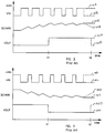
- the prior art filter circuit 10 is useful for eliminating only certain types of noise or glitches. With reference to the timing diagrams of FIGS. 2 and 3, it can be shown that a constant stream of noise pulses or "glitches" will not be filtered and will eventually lead to the occurrence of a false output signal.
- an input signal V IN is shown as a series of positive-going noise pulses, all of which pulses are desirably filtered out by a filter circuit.
- Input signal waveform 18A is a stream of noise pulses terminating at a "one" logic state, whereas input signal waveform 18B returns to a "zero" logic state.
- the analog integrated voltage of node 20 is labeled SCHMIN in FIG. 2, and includes corresponding waveforms 20A and 20B.
- the SCHMIN voltage is charged and discharged according to change in polarity of the input noise signal.
- the SCHMIN voltage periodically charges to the maximum available voltage, because of the duty cycle of the input signal.
- the maximum available voltage is the one logic state of the input voltage, typically the supply voltage of five volts.
- Waveform 20A shows the SCHMIN voltage finally charging to the supply voltage in response to the input signal staying at the one logic state, whereas waveform 20B shows the SCHMIN voltage discharging to zero volts in response to the input signal returning to the zero logic state.
- the Schmitt trigger 16 is characterized by having two distinct input threshold states, one for increasing input voltages, and another for decreasing input voltages.
- an input signal V IN is shown as a series of negative-going noise pulses, all of which pulses are desirably filtered out by a filter circuit.
- Input signal waveform 18C terminates in a zero logic state, whereas input signal waveform 18D terminates with the stream of noise pulses returning to a one logic state.
- the SCHMIN voltage charges and discharges in response to the input signal and eventually periodically discharges to the minimum available voltage, because of the duty cycle of the input signal.
- the minimum available voltage is the zero logic state of the input voltage, typically ground.
- Waveform 20C shows the SCHMIN voltage finally discharging to ground in response to the input signal staying at the zero logic state, whereas waveform 20D shows the SCHMIN voltage charging back to the supply voltage in response to the input signal returning to the one logic state.
- the SCHMIN voltage is discharged, at some time t1 the voltage crosses the input threshold voltage of Schmitt trigger 16, and a false output signal V OUT is generated.
- Output signal waveform 22C remains low, while output signal waveform 22D returns to a one logic state as the charging SCHMIN voltage crosses the other input threshold voltage of Schmitt trigger 16.
- a filter circuit includes an input node for receiving an unfiltered input signal, an output node for providing a filtered output signal, and an intermediate node.
- An integrator has an input coupled to the input node and an output coupled to the intermediate node.
- a Schmitt trigger has an input coupled to the intermediate node and an output coupled to the output node.
- a reset circuit has a first input coupled to the input node, a second input coupled to the output node, and an output coupled to the intermediate node. The signal on the intermediate node is generated by integrating the unfiltered logic input signal if the input signal and the output signal are at opposite logic states.
- a filtered output logic signal is generated by conditioning the intermediate signal with the Schmitt trigger.
- the reset circuit resets the intermediate signal if the input signal and the output signal are each at a zero logic state or if the input signal and the output signal are each at a one logic state, so that each new glitch or noise pulse starts the integration process anew and multiple noise pulses are thereby filtered.
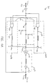
- a filter circuit 30 includes an input node 52 for receiving an unfiltered input signal designated V IN , an output node 56 for providing a filtered output signal designated V OUT , and an intermediate node 54 having an associated analog voltage designated SCHMIN (for Schmitt Trigger Input). While the schematic diagram of FIG. 4A shows a CMOS circuit, it should be appreciated by those skilled in the art that equivalent functionality can be obtained by other types of circuits such as bipolar circuits, for example.
- An optional input buffer stage 32 can be included to increase the input resistance of filter circuit 30 and to prevent loading of the input node 52, especially if input node 52 represents an input pin of an integrated circuit.
- Buffer stage 32 can also be used to "square up" analog or heavily loaded or otherwise distorted digital input signals. Buffer stage 32 can also be a "level translator” circuit if, for example, TTL input signals are present.
- Filter circuit 30 can be used to filter input signals presented at the input pin of an integrated circuit, or can be used to filter signals within an integrated circuit.
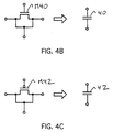
- Filter circuit 30 includes an integrator 33 consisting of a resistor 38, and capacitors 40 and 42. Turning momentarily to FIGS. 4B and 4C, in a preferred embodiment capacitors 40 and 42 are actually capacitor-connected MOS transistors. In FIG.
- capacitor 40 is shown as a capacitor-connected N-channel MOS transistor M40, wherein the gate of the transistor forms one of the capacitor plates, and the coupled drain and source form the other capacitor plate.
- capacitor 42 is shown as a capacitor-connected P-channel MOS transistor M42.
- capacitor 40 is coupled from node 54 to ground and capacitor 42 is coupled from node 54 to the supply voltage. In this manner, the voltage dependency of the capacitors is substantially cancelled. If voltage linear capacitors are available, then either capacitor 40 or 42 may be eliminated.
- Resistor 38 can be a thin film or diffused resistor, or any other resistor compatible with the integrated circuit process being used.
- a signal conditioning circuit 37 includes an inverting Schmitt trigger 48 in series with an inverter 50. Schmitt trigger 48 and inverter 50 are separate stages, which is standard in CMOS design. A single non-inverting Schmitt trigger conditioning circuit 37 can be substituted if other device technologies are used.
- the conditioning circuit can be a buffer stage, Schmitt trigger buffer stage, inverter stage, or Schmitt trigger inverter stage.
- the conditioning circuit 37 has an input coupled to the intermediate node 54 and an output coupled to the output node 56.
- a reset circuit 35 includes first and second parallel circuit portions 35A and 35B.
- the reset circuit 35 has a first input coupled to the input node 52 (directly or indirectly through optional input buffer stage 32), a second input coupled to the output node 56, and an output coupled to the intermediate node 54.
- the reset circuit 35 is a circuit that forces the intermediate node 54 to a low voltage if the input node 52 and the output node 56 are each at a zero logic state, and for forcing the intermediate node 54 to a high voltage if the input node 52 and the output node 56 are each at a one logic state.
- the first portion 35A of the reset circuit 35 includes a NAND gate 34 having two inputs and a single output. The two inputs of the NAND gate 34 form the first and second inputs of the first reset circuit portion 35A.
- a P-channel transistor 44 has a gate coupled to the output of the NAND gate 34, a source coupled to the five volt power supply voltage, and a drain forming the output of the first reset circuit portion 35A.
- the second portion 35B of the reset circuit 35 includes a NOR gate 36 having two inputs and a single output. The two inputs of the NOR gate 36 form the first and second inputs of the second reset circuit portion 35B.
- An N-channel transistor 46 has a gate coupled to the output of the NOR gate 36, a source coupled to ground, and a drain forming the output of the second reset circuit portion 35B.
- the filtering method of the present invention generally includes the steps of generating an unfiltered logic input signal V IN , which is provided to the filter circuit 30 at input node 52.
- An intermediate signal SCHMIN is generated by integrating the unfiltered logic input signal V IN if the input signal V IN and the output signal V OUT are at opposite logic states.
- a filtered output logic signal V OUT is generated by conditioning the intermediate signal SCHMIN.
- the intermediate signal SCHMIN is reset if the input signal V IN and the output signal V OUT are each at the same logic state.
- Filter circuit 30 is able to suppress glitches on noisy input signals having a number of closely spaced noise pulses, in order to prevent states changes from occurring in subsequent circuitry coupled to the output node 56.
- Input signals can therefore be extremely noisy and not adversely affect the operation of subsequent circuitry.
- Glitches and noise pulses are filtered for both positive-going and negative-going glitches, i.e. glitches are symmetrically filtered. The operation of the filter circuit is described in greater detail below.
- filter circuit 30 proceeds with reference to drawing FIGS. 4A, 5, 6, and 7. Assume that the input voltage V IN and the output voltage V OUT are both at a zero logic state, i.e. nodes 52 and 56 are at zero volt potential.
- the output of NOR gate 36 designated RESETLOW on node 60, is at a one logic state, which turns on transistor 46 and forces intermediate node 54 to ground.
- the output of NAND gate 34 designated RESETHIGH on node 58, is at a one logic state, which turns off transistor 44 and therefore this portion of the reset circuit exerts no control on node 54.
- node 54 will charge to a level that will trip Schmitt trigger 48 and cause the output, node 56, to switch to a one logic level.
- the output of NAND gate 34 switches to a zero logic level, turning on transistor 44, which in turn pulls intermediate node 54 to the supply voltage.
- filter circuit 30 The detailed operation of filter circuit 30 can thus be summarized according to the following table: Input Node 52 (V IN ) Output Node 56 (V OUT ) Int. Node 54 (SCHMIN) 0 0 0 0 1 Discharging 1 0 Charging 1 1 1
- filter circuit 30 is capable of filtering a number of closely spaced noise pulses or glitches.
- an input signal V IN is shown as a series of positive-going noise pulses, whose pulse width is less than a user-defined noise pulse width.
- Input signal waveform 52A is a stream of noise pulses terminating at a one logic state, whereas input signal waveform 52B returns to a zero logic state.
- the analog voltage of node 54 is labeled SCHMIN in FIG. 5, and includes corresponding waveforms 54A and 54B. Before time t3 in FIG. 5, the SCHMIN voltage is periodically charged to a voltage below the positive-going input threshold voltage of Schmitt trigger 48.
- the SCHMIN voltage is also periodically quickly discharged to ground when the noise pulses of the V IN voltage return to a zero logic state.
- Waveform 54A shows the SCHMIN voltage finally charging to the supply voltage in response to the input signal staying at the one logic state.
- the output voltage 56A waveform correctly and abruptly changes to a logic one state as the positive-going input voltage threshold of Schmitt trigger 48 is crossed.
- Waveform 54B shows the SCHMIN voltage again discharging to zero volts in response to the input signal returning to the zero logic state. In this case, the output waveform 56B remains at a zero logic state.
- an input signal V IN is shown as a series of negative-going noise pulses.
- Input signal waveform 52C is a stream of noise pulses terminating at a zero logic state, whereas input signal waveform 52D returns to a one logic state.
- the analog integrated voltage of node 54 is also labeled SCHMIN in FIG. 6, and includes corresponding waveforms 54C and 54D.
- the SCHMIN voltage is periodically discharged to a voltage above the negative-going input threshold voltage of Schmitt trigger 48.
- the SCHMIN voltage is also periodically quickly charged to the supply voltage when the noise pulses of the V IN voltage return to a one logic state.
- Waveform 54C shows the SCHMIN voltage finally discharging to ground in response to the input signal staying at the zero logic state.
- Waveform 54D shows the SCHMIN voltage again quickly charging to five volts in response to the input signal returning to the one logic state. In this case, the output waveform 56D remains at a one logic state.
- filter circuit 30 in response to a noiseless input pulse is shown in FIG. 7.
- the input signal waveform 52E changes from a zero logic state to a one logic state, and the SCHMIN waveform 54E begins to charge.
- the SCHMIN waveform 54E and the output signal waveform 56E abruptly switch to a one logic state.
- the input signal waveform 52E changes state to the orignal zero logic state, and the SCHMIN waveform 54E begins to discharge.
- the SCHMIN waveform 54E and the output waveform 56E abruptly switch.
Landscapes
- Physics & Mathematics (AREA)
- Nonlinear Science (AREA)
- Manipulation Of Pulses (AREA)
Applications Claiming Priority (2)
| Application Number | Priority Date | Filing Date | Title |
|---|---|---|---|
| US08/254,281 US5479132A (en) | 1994-06-06 | 1994-06-06 | Noise and glitch suppressing filter with feedback |
| US254281 | 1994-06-06 |
Publications (2)
| Publication Number | Publication Date |
|---|---|
| EP0687065A2 true EP0687065A2 (fr) | 1995-12-13 |
| EP0687065A3 EP0687065A3 (fr) | 1996-12-11 |
Family
ID=22963663
Family Applications (1)
| Application Number | Title | Priority Date | Filing Date |
|---|---|---|---|
| EP95303091A Withdrawn EP0687065A3 (fr) | 1994-06-06 | 1995-05-05 | Filtre de suppression d'impulsions de bruit avec contreaction |
Country Status (3)
| Country | Link |
|---|---|
| US (1) | US5479132A (fr) |
| EP (1) | EP0687065A3 (fr) |
| JP (1) | JPH07336201A (fr) |
Cited By (5)
| Publication number | Priority date | Publication date | Assignee | Title |
|---|---|---|---|---|
| EP0825715A1 (fr) * | 1996-08-19 | 1998-02-25 | Siemens Aktiengesellschaft | Circuit d'entrée pour des signaux numériques |
| FR2813460A1 (fr) * | 2000-08-24 | 2002-03-01 | St Microelectronics Sa | Circuit de filtrage de signaux logiques parasites |
| DE102006036348A1 (de) * | 2006-08-03 | 2008-02-07 | Infineon Technologies Ag | Schaltungsanordnung mit Filtern |
| WO2012135776A1 (fr) * | 2011-03-30 | 2012-10-04 | Qualcomm Incorporated | Filtre à impulsions étroites |
| EP2555429A1 (fr) * | 2011-08-04 | 2013-02-06 | Samsung Electro-Mechanics Co., Ltd | Circuit à semi-conducteur |
Families Citing this family (34)
| Publication number | Priority date | Publication date | Assignee | Title |
|---|---|---|---|---|
| US5444405A (en) * | 1992-03-02 | 1995-08-22 | Seiko Epson Corporation | Clock generator with programmable non-overlapping clock edge capability |
| US5929672A (en) * | 1995-06-16 | 1999-07-27 | Rohm Co., Ltd. | Power on reset circuit and one chip microcomputer using same |
| US5920221A (en) * | 1997-07-14 | 1999-07-06 | Vanguard International Semiconductor Corporation | RC delay circuit for integrated circuits |
| US6011419A (en) * | 1997-08-05 | 2000-01-04 | International Business Machines Corporation | Decoupling scheme for mixed voltage integrated circuits |
| US6191626B1 (en) * | 1998-08-17 | 2001-02-20 | Texas Instruments Incorporated | Method and apparatus for compensating input threshold variations on input buffers |
| TW483255B (en) * | 1999-11-26 | 2002-04-11 | Fujitsu Ltd | Phase-combining circuit and timing signal generator circuit for carrying out a high-speed signal transmission |
| US6538511B2 (en) * | 2001-03-06 | 2003-03-25 | Intersil Americas Inc. | Operational amplifier including a right-half plane zero reduction circuit and related method |
| US6606271B2 (en) * | 2001-05-23 | 2003-08-12 | Mircron Technology, Inc. | Circuit having a controllable slew rate |
| US6759880B2 (en) | 2002-06-13 | 2004-07-06 | Hewlett-Packard Development Company, L.P. | Driver circuit connected to a switched capacitor and method of operating same |
| US6753708B2 (en) * | 2002-06-13 | 2004-06-22 | Hewlett-Packard Development Company, L.P. | Driver circuit connected to pulse shaping circuitry and method of operating same |
| JP2005057217A (ja) * | 2003-08-07 | 2005-03-03 | Renesas Technology Corp | 半導体集積回路装置 |
| TW200509533A (en) * | 2003-08-25 | 2005-03-01 | Holtek Semiconductor Inc | Inhibition device for high-frequency signal |
| US6894540B1 (en) | 2003-12-17 | 2005-05-17 | Freescale Semiconductor, Inc. | Glitch removal circuit |
| US20050134323A1 (en) * | 2003-12-23 | 2005-06-23 | Honeywell International Inc. | Single event transient filter for comparator |
| TWI229498B (en) * | 2004-01-09 | 2005-03-11 | Via Tech Inc | Low pass filter de-glitch circuit |
| US20050179468A1 (en) * | 2004-02-17 | 2005-08-18 | Binling Zhou | Implementation of MOS capacitor in CT scanner data acquisition system |
| JP4738945B2 (ja) | 2005-09-06 | 2011-08-03 | フリースケール セミコンダクター インコーポレイテッド | デグリッチ回路 |
| JP4855748B2 (ja) * | 2005-09-28 | 2012-01-18 | 株式会社リコー | 遅延回路及び遅延回路を使用した電源システム装置 |
| US7397292B1 (en) * | 2006-06-21 | 2008-07-08 | National Semiconductor Corporation | Digital input buffer with glitch suppression |
| US8692576B2 (en) * | 2006-09-18 | 2014-04-08 | Linear Technology Corporation | Circuit and methodology for high-speed, low-power level shifting |
| TWI330946B (en) * | 2007-03-12 | 2010-09-21 | Via Tech Inc | Phase-locked loop and compound mos capacitor thereof |
| JP2010056677A (ja) * | 2008-08-26 | 2010-03-11 | Fujitsu Ltd | デューティ可変回路 |
| US8779857B2 (en) * | 2009-08-14 | 2014-07-15 | Qualcomm Incorporated | Amplifier with variable matching circuit to improve linearity |
| EP2354882B1 (fr) * | 2010-02-10 | 2017-04-26 | Nxp B.V. | Circuit et procédé de source de courant commutable |
| US20120126864A1 (en) * | 2010-11-22 | 2012-05-24 | Tyler Daigle | Power-on reset |
| US8710908B2 (en) | 2011-01-28 | 2014-04-29 | Taiwan Semiconductor Manufacturing Company, Ltd. | Charge pump and method of biasing deep N-well in charge pump |
| US20140043089A1 (en) * | 2011-04-28 | 2014-02-13 | Koninklijke Philips N.V. | Digitally controlled high speed high voltage gate driver circuit |
| US8698480B2 (en) * | 2011-06-27 | 2014-04-15 | Micron Technology, Inc. | Reference current distribution |
| US9671801B2 (en) * | 2013-11-06 | 2017-06-06 | Dialog Semiconductor Gmbh | Apparatus and method for a voltage regulator with improved power supply reduction ratio (PSRR) with reduced parasitic capacitance on bias signal lines |
| KR101942726B1 (ko) * | 2014-03-17 | 2019-01-28 | 삼성전기 주식회사 | 액티브 노이즈 필터 장치 및 이를 갖는 게이트 구동 장치 |
| US10461749B1 (en) * | 2018-10-25 | 2019-10-29 | Shenzhen GOODIX Technology Co., Ltd. | Ground intermediation for inter-domain buffer stages |
| US12237836B2 (en) * | 2022-03-31 | 2025-02-25 | Texas Instruments Incorporated | Signal chatter mitigation |
| TWI829286B (zh) * | 2022-08-12 | 2024-01-11 | 新唐科技股份有限公司 | 無短時脈衝波的低通濾波電路與使用其的系統電路 |
| CN116827330B (zh) * | 2022-12-12 | 2024-03-12 | 南京微盟电子有限公司 | 强抗干扰通讯端口电路 |
Family Cites Families (9)
| Publication number | Priority date | Publication date | Assignee | Title |
|---|---|---|---|---|
| US3822385A (en) * | 1973-09-14 | 1974-07-02 | Bell Northern Research Ltd | Noise pulse rejection circuit |
| US4045688A (en) * | 1976-10-26 | 1977-08-30 | Rca Corporation | Power-on reset circuit |
| JPS6019855B2 (ja) * | 1978-08-02 | 1985-05-18 | 株式会社東精エンジニアリングサ−ビス | 起伏する入力信号の計数回路 |
| US4471235A (en) * | 1982-05-03 | 1984-09-11 | Data General Corporation | Short pulse width noise immunity discriminator circuit |
| DE3225800C1 (de) * | 1982-07-09 | 1983-12-15 | Siemens AG, 1000 Berlin und 8000 München | Schaltungsanordnung zur Störbefreiung von binären Signalen |
| JPS61281616A (ja) * | 1985-06-07 | 1986-12-12 | Hitachi Ltd | パルス検出回路 |
| KR970000560B1 (ko) * | 1986-10-01 | 1997-01-13 | 아오이 죠이치 | 반도체집적회로 |
| JP2653177B2 (ja) * | 1989-06-22 | 1997-09-10 | 日産自動車株式会社 | 雑音除去回路 |
| US5324999A (en) * | 1992-10-27 | 1994-06-28 | Texas Instruments Incorporated | Input buffer with compensated low-pass filter network |
-
1994
- 1994-06-06 US US08/254,281 patent/US5479132A/en not_active Expired - Fee Related
-
1995
- 1995-05-05 EP EP95303091A patent/EP0687065A3/fr not_active Withdrawn
- 1995-06-05 JP JP7137572A patent/JPH07336201A/ja active Pending
Cited By (9)
| Publication number | Priority date | Publication date | Assignee | Title |
|---|---|---|---|---|
| EP0825715A1 (fr) * | 1996-08-19 | 1998-02-25 | Siemens Aktiengesellschaft | Circuit d'entrée pour des signaux numériques |
| FR2813460A1 (fr) * | 2000-08-24 | 2002-03-01 | St Microelectronics Sa | Circuit de filtrage de signaux logiques parasites |
| US6507221B2 (en) | 2000-08-24 | 2003-01-14 | Stmicroelectronics S.A. | Circuit for the filtering of parasitic logic signals |
| DE102006036348A1 (de) * | 2006-08-03 | 2008-02-07 | Infineon Technologies Ag | Schaltungsanordnung mit Filtern |
| WO2012135776A1 (fr) * | 2011-03-30 | 2012-10-04 | Qualcomm Incorporated | Filtre à impulsions étroites |
| EP2555429A1 (fr) * | 2011-08-04 | 2013-02-06 | Samsung Electro-Mechanics Co., Ltd | Circuit à semi-conducteur |
| CN102916688A (zh) * | 2011-08-04 | 2013-02-06 | 三星电机株式会社 | 半导体电路 |
| US8674740B2 (en) | 2011-08-04 | 2014-03-18 | Samsung Electro-Mechanics Co., Ltd. | Noise removing delay circuit |
| CN102916688B (zh) * | 2011-08-04 | 2015-04-29 | 三星电机株式会社 | 半导体电路 |
Also Published As
| Publication number | Publication date |
|---|---|
| EP0687065A3 (fr) | 1996-12-11 |
| JPH07336201A (ja) | 1995-12-22 |
| US5479132A (en) | 1995-12-26 |
Similar Documents
| Publication | Publication Date | Title |
|---|---|---|
| US5479132A (en) | Noise and glitch suppressing filter with feedback | |
| EP0150480B1 (fr) | Générateur d'impulsion pour l'établissement de l'état initial à l'enclenchement du secteur | |
| US4620312A (en) | Pulse signal processing circuit | |
| EP1469603A1 (fr) | Buffer de sortie à temps de montée commandée | |
| EP1199790A2 (fr) | Alimentation de puissance avec un système de commande à modulation de largeur d'impulsion | |
| JP3005169B2 (ja) | リセット回路 | |
| JPH0511805B2 (fr) | ||
| US6750685B1 (en) | Apparatus and method for a bi-directional charge driver circuit | |
| US6016070A (en) | Pulse extending circuit | |
| US6873216B2 (en) | Chattering eliminating apparatus including oscillation circuit using charging and discharging operations | |
| EP0433724A2 (fr) | Régulateur de tension avec système agrégat additionnel de puissance | |
| US7084684B2 (en) | Delay stage insensitive to operating voltage and delay circuit including the same | |
| Bazarjani et al. | Low voltage SC circuit design with low-V/sub t/MOSFETs | |
| EP0739095A1 (fr) | Détecteur de tension d'alimentation | |
| US6756831B2 (en) | Wide dynamic pulse width modulation neuron circuit | |
| EP0540661A1 (fr) | Alimentation miniaturisee en courant de commutation comprenant un filtre d'ecretage unidirectionnel. | |
| US20200304125A1 (en) | Power supply detection circuit | |
| JPH10313240A (ja) | パワーオンリセット回路 | |
| EP0608666B1 (fr) | Circuit à retard de temps monolithiquement intégrable | |
| JP2680592B2 (ja) | パワーオンリセット回路 | |
| US6339345B1 (en) | Semiconductor device equipped with output circuit adjusting duration of high and low levels | |
| JP3647302B2 (ja) | パワーオンリセット回路及び、これを備えた集積回路装置 | |
| JPH05167424A (ja) | 出力バッファ回路 | |
| JPH0329411A (ja) | 遅延回路 | |
| KR930009425B1 (ko) | 시스템 초기리세트회로 |
Legal Events
| Date | Code | Title | Description |
|---|---|---|---|
| PUAI | Public reference made under article 153(3) epc to a published international application that has entered the european phase |
Free format text: ORIGINAL CODE: 0009012 |
|
| AK | Designated contracting states |
Kind code of ref document: A2 Designated state(s): DE FR GB |
|
| PUAL | Search report despatched |
Free format text: ORIGINAL CODE: 0009013 |
|
| AK | Designated contracting states |
Kind code of ref document: A3 Designated state(s): DE FR GB |
|
| STAA | Information on the status of an ep patent application or granted ep patent |
Free format text: STATUS: THE APPLICATION IS DEEMED TO BE WITHDRAWN |
|
| 18D | Application deemed to be withdrawn |
Effective date: 19970612 |