EP0688052A2 - Verbesserungen in der oder in Bezug auf die Herstellung einer Halbleiteranordnung - Google Patents
Verbesserungen in der oder in Bezug auf die Herstellung einer Halbleiteranordnung Download PDFInfo
- Publication number
- EP0688052A2 EP0688052A2 EP95107519A EP95107519A EP0688052A2 EP 0688052 A2 EP0688052 A2 EP 0688052A2 EP 95107519 A EP95107519 A EP 95107519A EP 95107519 A EP95107519 A EP 95107519A EP 0688052 A2 EP0688052 A2 EP 0688052A2
- Authority
- EP
- European Patent Office
- Prior art keywords
- conductors
- porous dielectric
- layer
- porous
- dielectric layer
- Prior art date
- Legal status (The legal status is an assumption and is not a legal conclusion. Google has not performed a legal analysis and makes no representation as to the accuracy of the status listed.)
- Ceased
Links
Images


Classifications
-
- H—ELECTRICITY
- H10—SEMICONDUCTOR DEVICES; ELECTRIC SOLID-STATE DEVICES NOT OTHERWISE PROVIDED FOR
- H10P—GENERIC PROCESSES OR APPARATUS FOR THE MANUFACTURE OR TREATMENT OF DEVICES COVERED BY CLASS H10
- H10P14/00—Formation of materials, e.g. in the shape of layers or pillars
- H10P14/60—Formation of materials, e.g. in the shape of layers or pillars of insulating materials
- H10P14/65—Formation of materials, e.g. in the shape of layers or pillars of insulating materials characterised by treatments performed before or after the formation of the materials
- H10P14/6516—Formation of materials, e.g. in the shape of layers or pillars of insulating materials characterised by treatments performed before or after the formation of the materials of treatments performed after formation of the materials
- H10P14/6548—Formation of materials, e.g. in the shape of layers or pillars of insulating materials characterised by treatments performed before or after the formation of the materials of treatments performed after formation of the materials by forming intermediate materials, e.g. capping layers or diffusion barriers
-
- H—ELECTRICITY
- H10—SEMICONDUCTOR DEVICES; ELECTRIC SOLID-STATE DEVICES NOT OTHERWISE PROVIDED FOR
- H10P—GENERIC PROCESSES OR APPARATUS FOR THE MANUFACTURE OR TREATMENT OF DEVICES COVERED BY CLASS H10
- H10P14/00—Formation of materials, e.g. in the shape of layers or pillars
- H10P14/60—Formation of materials, e.g. in the shape of layers or pillars of insulating materials
- H10P14/65—Formation of materials, e.g. in the shape of layers or pillars of insulating materials characterised by treatments performed before or after the formation of the materials
- H10P14/6516—Formation of materials, e.g. in the shape of layers or pillars of insulating materials characterised by treatments performed before or after the formation of the materials of treatments performed after formation of the materials
- H10P14/6546—Formation of materials, e.g. in the shape of layers or pillars of insulating materials characterised by treatments performed before or after the formation of the materials of treatments performed after formation of the materials to change the surface groups of the insulating materials
-
- H—ELECTRICITY
- H10—SEMICONDUCTOR DEVICES; ELECTRIC SOLID-STATE DEVICES NOT OTHERWISE PROVIDED FOR
- H10P—GENERIC PROCESSES OR APPARATUS FOR THE MANUFACTURE OR TREATMENT OF DEVICES COVERED BY CLASS H10
- H10P14/00—Formation of materials, e.g. in the shape of layers or pillars
- H10P14/60—Formation of materials, e.g. in the shape of layers or pillars of insulating materials
- H10P14/66—Formation of materials, e.g. in the shape of layers or pillars of insulating materials characterised by the type of materials
- H10P14/668—Formation of materials, e.g. in the shape of layers or pillars of insulating materials characterised by the type of materials the materials being characterised by the deposition precursor materials
- H10P14/6681—Formation of materials, e.g. in the shape of layers or pillars of insulating materials characterised by the type of materials the materials being characterised by the deposition precursor materials the precursor containing a compound comprising Si
- H10P14/6684—Formation of materials, e.g. in the shape of layers or pillars of insulating materials characterised by the type of materials the materials being characterised by the deposition precursor materials the precursor containing a compound comprising Si the compound comprising silicon and oxygen
- H10P14/6686—Formation of materials, e.g. in the shape of layers or pillars of insulating materials characterised by the type of materials the materials being characterised by the deposition precursor materials the precursor containing a compound comprising Si the compound comprising silicon and oxygen the compound being a molecule comprising at least one silicon-oxygen bond and the compound having hydrogen or an organic group attached to the silicon or oxygen, e.g. a siloxane
-
- H—ELECTRICITY
- H10—SEMICONDUCTOR DEVICES; ELECTRIC SOLID-STATE DEVICES NOT OTHERWISE PROVIDED FOR
- H10P—GENERIC PROCESSES OR APPARATUS FOR THE MANUFACTURE OR TREATMENT OF DEVICES COVERED BY CLASS H10
- H10P14/00—Formation of materials, e.g. in the shape of layers or pillars
- H10P14/60—Formation of materials, e.g. in the shape of layers or pillars of insulating materials
- H10P14/69—Inorganic materials
- H10P14/6903—Inorganic materials containing silicon
-
- H—ELECTRICITY
- H10—SEMICONDUCTOR DEVICES; ELECTRIC SOLID-STATE DEVICES NOT OTHERWISE PROVIDED FOR
- H10W—GENERIC PACKAGES, INTERCONNECTIONS, CONNECTORS OR OTHER CONSTRUCTIONAL DETAILS OF DEVICES COVERED BY CLASS H10
- H10W20/00—Interconnections in chips, wafers or substrates
- H10W20/01—Manufacture or treatment
- H10W20/071—Manufacture or treatment of dielectric parts thereof
- H10W20/072—Manufacture or treatment of dielectric parts thereof of dielectric parts comprising air gaps
-
- H—ELECTRICITY
- H10—SEMICONDUCTOR DEVICES; ELECTRIC SOLID-STATE DEVICES NOT OTHERWISE PROVIDED FOR
- H10W—GENERIC PACKAGES, INTERCONNECTIONS, CONNECTORS OR OTHER CONSTRUCTIONAL DETAILS OF DEVICES COVERED BY CLASS H10
- H10W20/00—Interconnections in chips, wafers or substrates
- H10W20/01—Manufacture or treatment
- H10W20/071—Manufacture or treatment of dielectric parts thereof
- H10W20/074—Manufacture or treatment of dielectric parts thereof of dielectric parts comprising thin functional dielectric layers, e.g. dielectric etch-stop, barrier, capping or liner layers
- H10W20/077—Manufacture or treatment of dielectric parts thereof of dielectric parts comprising thin functional dielectric layers, e.g. dielectric etch-stop, barrier, capping or liner layers on sidewalls or on top surfaces of conductors
-
- H—ELECTRICITY
- H10—SEMICONDUCTOR DEVICES; ELECTRIC SOLID-STATE DEVICES NOT OTHERWISE PROVIDED FOR
- H10W—GENERIC PACKAGES, INTERCONNECTIONS, CONNECTORS OR OTHER CONSTRUCTIONAL DETAILS OF DEVICES COVERED BY CLASS H10
- H10W20/00—Interconnections in chips, wafers or substrates
- H10W20/40—Interconnections external to wafers or substrates, e.g. back-end-of-line [BEOL] metallisations or vias connecting to gate electrodes
- H10W20/41—Interconnections external to wafers or substrates, e.g. back-end-of-line [BEOL] metallisations or vias connecting to gate electrodes characterised by their conductive parts
- H10W20/42—Vias, e.g. via plugs
-
- H—ELECTRICITY
- H10—SEMICONDUCTOR DEVICES; ELECTRIC SOLID-STATE DEVICES NOT OTHERWISE PROVIDED FOR
- H10W—GENERIC PACKAGES, INTERCONNECTIONS, CONNECTORS OR OTHER CONSTRUCTIONAL DETAILS OF DEVICES COVERED BY CLASS H10
- H10W20/00—Interconnections in chips, wafers or substrates
- H10W20/40—Interconnections external to wafers or substrates, e.g. back-end-of-line [BEOL] metallisations or vias connecting to gate electrodes
- H10W20/41—Interconnections external to wafers or substrates, e.g. back-end-of-line [BEOL] metallisations or vias connecting to gate electrodes characterised by their conductive parts
- H10W20/435—Cross-sectional shapes or dispositions of interconnections
-
- H—ELECTRICITY
- H10—SEMICONDUCTOR DEVICES; ELECTRIC SOLID-STATE DEVICES NOT OTHERWISE PROVIDED FOR
- H10W—GENERIC PACKAGES, INTERCONNECTIONS, CONNECTORS OR OTHER CONSTRUCTIONAL DETAILS OF DEVICES COVERED BY CLASS H10
- H10W20/00—Interconnections in chips, wafers or substrates
- H10W20/40—Interconnections external to wafers or substrates, e.g. back-end-of-line [BEOL] metallisations or vias connecting to gate electrodes
- H10W20/45—Interconnections external to wafers or substrates, e.g. back-end-of-line [BEOL] metallisations or vias connecting to gate electrodes characterised by their insulating parts
- H10W20/46—Interconnections external to wafers or substrates, e.g. back-end-of-line [BEOL] metallisations or vias connecting to gate electrodes characterised by their insulating parts comprising air gaps
-
- H—ELECTRICITY
- H10—SEMICONDUCTOR DEVICES; ELECTRIC SOLID-STATE DEVICES NOT OTHERWISE PROVIDED FOR
- H10W—GENERIC PACKAGES, INTERCONNECTIONS, CONNECTORS OR OTHER CONSTRUCTIONAL DETAILS OF DEVICES COVERED BY CLASS H10
- H10W20/00—Interconnections in chips, wafers or substrates
- H10W20/40—Interconnections external to wafers or substrates, e.g. back-end-of-line [BEOL] metallisations or vias connecting to gate electrodes
- H10W20/45—Interconnections external to wafers or substrates, e.g. back-end-of-line [BEOL] metallisations or vias connecting to gate electrodes characterised by their insulating parts
- H10W20/48—Insulating materials thereof
-
- H—ELECTRICITY
- H10—SEMICONDUCTOR DEVICES; ELECTRIC SOLID-STATE DEVICES NOT OTHERWISE PROVIDED FOR
- H10W—GENERIC PACKAGES, INTERCONNECTIONS, CONNECTORS OR OTHER CONSTRUCTIONAL DETAILS OF DEVICES COVERED BY CLASS H10
- H10W20/00—Interconnections in chips, wafers or substrates
- H10W20/40—Interconnections external to wafers or substrates, e.g. back-end-of-line [BEOL] metallisations or vias connecting to gate electrodes
- H10W20/495—Capacitive arrangements or effects of, or between wiring layers
-
- H—ELECTRICITY
- H10—SEMICONDUCTOR DEVICES; ELECTRIC SOLID-STATE DEVICES NOT OTHERWISE PROVIDED FOR
- H10P—GENERIC PROCESSES OR APPARATUS FOR THE MANUFACTURE OR TREATMENT OF DEVICES COVERED BY CLASS H10
- H10P14/00—Formation of materials, e.g. in the shape of layers or pillars
- H10P14/60—Formation of materials, e.g. in the shape of layers or pillars of insulating materials
- H10P14/63—Formation of materials, e.g. in the shape of layers or pillars of insulating materials characterised by the formation processes
- H10P14/6326—Deposition processes
- H10P14/6342—Liquid deposition, e.g. spin-coating, sol-gel techniques or spray coating
-
- H—ELECTRICITY
- H10—SEMICONDUCTOR DEVICES; ELECTRIC SOLID-STATE DEVICES NOT OTHERWISE PROVIDED FOR
- H10P—GENERIC PROCESSES OR APPARATUS FOR THE MANUFACTURE OR TREATMENT OF DEVICES COVERED BY CLASS H10
- H10P14/00—Formation of materials, e.g. in the shape of layers or pillars
- H10P14/60—Formation of materials, e.g. in the shape of layers or pillars of insulating materials
- H10P14/66—Formation of materials, e.g. in the shape of layers or pillars of insulating materials characterised by the type of materials
- H10P14/665—Porous materials
-
- H—ELECTRICITY
- H10—SEMICONDUCTOR DEVICES; ELECTRIC SOLID-STATE DEVICES NOT OTHERWISE PROVIDED FOR
- H10P—GENERIC PROCESSES OR APPARATUS FOR THE MANUFACTURE OR TREATMENT OF DEVICES COVERED BY CLASS H10
- H10P14/00—Formation of materials, e.g. in the shape of layers or pillars
- H10P14/60—Formation of materials, e.g. in the shape of layers or pillars of insulating materials
- H10P14/69—Inorganic materials
- H10P14/692—Inorganic materials composed of oxides, glassy oxides or oxide-based glasses
- H10P14/6921—Inorganic materials composed of oxides, glassy oxides or oxide-based glasses containing silicon
- H10P14/6922—Inorganic materials composed of oxides, glassy oxides or oxide-based glasses containing silicon the material containing Si, O and at least one of H, N, C, F or other non-metal elements, e.g. SiOC, SiOC:H or SiONC
-
- Y—GENERAL TAGGING OF NEW TECHNOLOGICAL DEVELOPMENTS; GENERAL TAGGING OF CROSS-SECTIONAL TECHNOLOGIES SPANNING OVER SEVERAL SECTIONS OF THE IPC; TECHNICAL SUBJECTS COVERED BY FORMER USPC CROSS-REFERENCE ART COLLECTIONS [XRACs] AND DIGESTS
- Y10—TECHNICAL SUBJECTS COVERED BY FORMER USPC
- Y10S—TECHNICAL SUBJECTS COVERED BY FORMER USPC CROSS-REFERENCE ART COLLECTIONS [XRACs] AND DIGESTS
- Y10S148/00—Metal treatment
- Y10S148/043—Dual dielectric
-
- Y—GENERAL TAGGING OF NEW TECHNOLOGICAL DEVELOPMENTS; GENERAL TAGGING OF CROSS-SECTIONAL TECHNOLOGIES SPANNING OVER SEVERAL SECTIONS OF THE IPC; TECHNICAL SUBJECTS COVERED BY FORMER USPC CROSS-REFERENCE ART COLLECTIONS [XRACs] AND DIGESTS
- Y10—TECHNICAL SUBJECTS COVERED BY FORMER USPC
- Y10S—TECHNICAL SUBJECTS COVERED BY FORMER USPC CROSS-REFERENCE ART COLLECTIONS [XRACs] AND DIGESTS
- Y10S148/00—Metal treatment
- Y10S148/118—Oxide films
Definitions
- This invention relates generally to the fabrication of dielectrics on semiconductor devices, and more particularly to methods and structures for reducing capacitive coupling on a semiconductor device using electrical insulators made of porous dielectric materials.
- Semiconductors are widely used in integrated circuits for electronic devices such as computers and televisions. These integrated circuits typically combine many transistors on a single crystal silicon chip to perform complex functions and store data. Semiconductor and electronics manufacturers, as well as end users, desire integrated circuits which can accomplish more in less time in a smaller package while consuming less power. However, many of these desires are in opposition to each other. For instance, simply shrinking the feature size on a given circuit from 0.5 microns to 0.25 microns can increase power consumption by 30%. Likewise, doubling operational speed generally doubles power consumption. Miniaturization also generally results in increased capacitive coupling, or crosstalk, between conductors which carry signals across the chip. This effect both limits achievable speed and degrades the noise margin used to insure proper device operation.
- U.S. Pat. No. 4,987,101 issued to Kaanta et al., on Jan. 22, 1991, describes a method for fabricating gas (air) dielectrics, which comprises depositing a temporary layer of removable material between supports (such as conductors), covering this with a capping insulator layer, opening access holes in the cap, extracting the removable material through these access holes, then closing the access holes.
- This method can be cumbersome, partially because it requires consideration of access hole locations in the design rules and alignment error budget during circuit design, as well as requiring extra processing steps to create and then plug the holes.
- This method may also create large void areas which have essentially no means of handling mechanical stress and heat dissipation.
- This structure is typically formed by depositing a mixture of an acidic oxide and a basic oxide, heat treating to precipitate the basic oxide, and then dissolving out the basic oxide. Dissolving all of the basic oxide out of such a structure may be problematic, because small pockets of the basic oxide may not be reached by the leaching agent.
- Dielectrics formed by this method are typically 15% to 50% porous, with a permanent film thickness reduction of at least 20% during drying.
- the higher porosities e.g. 40-50%) can only be achieved at pore sizes which are generally too large for such microcircuit applications.
- These materials are usually referred to as xerogels, although the final structure is not a gel, but an open-pored (the pores are generally interconnected, rather than being isolated cells) porous structure of a solid material.
- the present invention provides novel structures and methods for hybrid porous/non-porous dielectrics for use as semiconductor insulators.
- the structures combine a low dielectric constant (k generally less than 3.0 and preferably less than 2.0) porous material with non-porous dielectric materials in a manner which emphasizes the desirable aspects of both, for the primary purpose of decreasing unwanted capacitance between conductors formed on a semiconductor device.
- k generally less than 3.0 and preferably less than 2.0
- One of the problems recognized herein is the difficulty in producing devices with significant structure formed after the porous layer. By the methods of this invention, even multiple porous layers are possible, and construction of the device can be accomplished by sequential layered techniques.
- porous dielectrics recognized herein include: decreased mechanical strength and thermal conductivity compared to solid silicon dioxide; difficulty with anisotropic (directional) etching typically required for via formation; difficulty in forming patterned layers on top of porous layers; the hydrophilic (water-wanting) nature of many finely-pored (and especially silica) dielectrics; and general unsuitability of known porous dielectric-forming methods to practical submicron device construction. Methods and structures disclosed herein allow solution to these and other problems.
- the present invention can provide a method for constructing a semiconductor device, with a primary purpose of decreasing unwanted capacitance between conductors formed on the device.
- the method can comprise providing a layer of patterned conductors formed on a semiconductor substrate, and forming a porous dielectric layer filling gaps between and covering the patterned conductors.
- the method can further comprise removing a top portion of the porous dielectric layer to expose at least the tops of the conductors.
- the method can further comprise depositing a non-porous dielectric layer over the conductors and porous layer. This non-porous layer is preferably comprised of a bottom sublayer conformally formed by e.g.
- the method can further comprise creating one or more metal-filled vias passing through the non-porous layer to provide electrical contact to the patterned conductors, and forming a second layer of conductors on top of this structure.
- the present invention can also provide structures for semiconductor devices with reduced intralayer capacitance, comprising at least a first and second conductor formed on a semiconductor substrate, with a porous dielectric between the first and second conductors.
- the porous dielectric preferably has an average height of 75% to 150% the height of the conductors.
- the porous dielectric also preferably has an average pore diameter of less than 80 nm (more preferably between 2 nm and 25 nm).
- the porous dielectric also preferably has a porosity between 30% and 95% (more preferably between 50% and 75%).
- the device may further comprise a non-porous dielectric layer deposited over the tops of the conductors and the porous dielectric, preferably at least 50% the height of the conductors, as measured over a conductor.
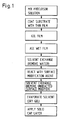
- Typical embodiments of the invention are described with a porous dielectric method which may be comprised of the steps shown in Figure 1 , although not all steps shown may be required in a given embodiment. Furthermore, materials may be substituted in several of the steps to achieve various effects, and processing parameters such as times, temperatures, pressures, and relative concentrations of ingredients may be varied over broad ranges. In any case, another method which produces a similar porous dielectric layer could be substituted for the method of Figure 1 .
- various precursor solutions (some of which are described in detail in the specific examples) may be mixed, and then applied to a substrate upon which a layer of patterned conductors has been formed. The method of application may be, for example, a spin-on technique in a controlled atmosphere which limits solvent evaporation.
- the object of the application in at least one embodiment is to form a layer of the precursor which will at least substantially fill the gaps between adjacent conductors.
- the precursor solution is allowed to gel on the substrate, a process which typically takes from 1 minute to 12 hours, depending on the solution and method of gelling.
- the wet gel can be allowed time to age, generally about a day (although it may be much shorter), at one or more controlled temperatures. If the wet gel contains water, one or more washing steps can be used to perform a solvent exchange on the gel, thereby removing the water but leaving the gel in a wet state.
- the solvent may be either a protic (e.g. ethanol) or an aprotic (e.g. acetone or hexane) solvent.
- the wet gel may then be reacted with a surface modification agent (the effects of the surface modification step will be explained below) by a method such as immersing the structure in a mixture containing the surface modification agent and a solvent in which the modification agent is soluble. This solvent must also be miscible with the solvent already present in the wet gel. Another solvent exchange may be subsequently used to remove excess surface modification agent from the structure. The solvent is allowed to evaporate out of the gel, leaving a porous dielectric structure. If the film is substantially undensified during drying, the dried gel exhibits essentially the same structure as the wet gel (the dried film thickness is substantially the same as the wet gel film thickness). The porous dielectric may finally be capped with a non-porous insulation layer, as detailed in the specific examples.
- FIG. 2A a cross-section of a single pore 12 in a wet gel structure 10 is shown, with a liquid pore fluid 14 filling pore 12 .
- Figure 2B shows the same pore undergoing evaporation of the pore fluid.
- a phase change (from liquid to vapor) is illustrated by the formation of a meniscus 18 , which is shown as a crescent-shaped boundary between liquid pore fluid 14 and vapor 16 formed during evaporation.
- the meniscus is an indication of the surface tension of the pore fluid exerting an inward (usually, although some fluids can exert outward) pressure on the walls of the pore.
- This capillary pressure P can be related to the pore fluid surface tension Ts , the contact angle q (the angle at which the fluid meniscus contacts the surface of the pore), and the pore radius r , by the equation
- the difficulty in maintaining the integrity of extremely small pores (small r ) during drying is evident from this equation, since every halving of radius r doubles the pressure on the pore walls.
- a porous dielectric suitable for use between conductors should contain pores at least an order of magnitude smaller than the interconductor gap ( r approximately 10 nanometers for a 0.2 micron gap, for example). Adjusting pore size upwards to relieve capillary pressure is therefore a limited option for microelectronic applications.
- simply allowing pores to collapse from the capillary pressure results in excessive shrinkage, with the corresponding densification of the dielectric defeating the primary purpose of the method (reducing dielectric constant) as well as preventing good surface adhesion.
- the aerogel technique has been developed.
- this variation of the xerogel technique removes a solvent from a wet gel under supercritical pressure and temperature conditions. By removing the solvent in the supercritical region, vaporization of the liquid solvent does not take place; instead, the fluid undergoes a constant change in density during the operation, changing from a compressed liquid to a superheated vapor with no distinguishable state boundary.
- This technique avoids the capillary pressure problem entirely, since no state change boundaries ever exist in the pores.
- Adapting the aerogel technique to semiconductor fabrication appears to be problematic and expensive; typical solvent candidates have high critical pressures (e.g.
- ethanol, 924 psi, carbon dioxide, 1071 psi which make application difficult in most circumstances.
- these pressures may tend to crush previous layers of porous dielectric capped under atmospheric pressure or force the wet gel into the pores of previous porous dielectric layers left uncapped, and may require containment of the wet gel at the edges of the wafer to prevent the gel from being squeezed off the wafer before the gel can be dried.
- a highly porous, finely pored dielectric structure may be formed by this process under some conditions, making this supercritical technique possibly useful in the practice of the present invention.
- the present invention includes a group of novel techniques which may be applied at a range of pressures from vacuum to near-critical, with atmospheric pressure being preferable due to ease of handling and compatibility with previous porous layers.
- One similarity in these techniques is that a surface modification step is performed on the wet gel, replacing a substantial number of the molecules on the pore walls with those of another species.
- This surface modification typically replaces reactive surface groups such as hydroxyls and alkoxyls with more stable surface groups such as methyl groups, thereby controlling undesirable condensation reactions (and shrinkage effects) during gel drying.
- Figure 2C shows a cross-section of a pore after the surface modification step; portions of gel 10 which are on the surface of pore 12 (labeled as region 20 ) now contain a different species.
- the final shrinkage may be adjusted from the large shinkage typical of an unmodified xerogel (with uncontrolled shrinkage) to a shrinkage of only a few percent, heretofore only achievable with an aerogel technique.
- approximately 30% of the reactive surface groups must be replaced to substantially alleviate densification.
- the replacement surface species may be chosen because of its wetting properties in combination with specific pore fluids; thus in Figure 2D , meniscus 18 is significantly flatter than that of Figure 2B , resulting in a pore fluid contact angle closer to 90 degrees.
- the cosine of the contact angle q goes to 0, and the capillary pressure P of Equation 1 is reduced proportionally. It is believed that the surface modification prevents surface condensation reactions, and may also reduce capillary pressure by changing pore fluid contact angle, thereby allowing pores in the surface modified gel to better survive drying.
- This novel technique can produce a dielectric layer, at atmospheric pressure, with average pore diameter, porosity, and overall shrinkage resembling those of supercritically-dried aerogels.
- An additional benefit of the surface modification can be hydrophobicity. It has been found that, for example, replacing only 15% of the reactive surface groups with methyl groups may be sufficient to cause the structure to be hydrophobic. This is an important feature for any material used in semiconductor processing, but particularly so for porous materials. If the porous surfaces are left hydrophilic (water-wanting), the structure is in many ways analagous to a common household sponge, which may hold many times its weight in water. However, the extremely small pore sizes allow a hydrophilic porous dielectric to rapidly gather water out of the surrounding air, the prevention of which would be an added difficulty during device fabrication. By making the pores hydrophobic before the gel is dried, these types of difficulties may be avoided.
- Figures 3A-3D show cross-sections of a semiconductor device at various stages during fabrication.
- use of the word wafer will imply a wafer as used in conventional semiconductor processing, with at least the illustrated semiconductor device incorporated therein.
- three patterned conductors 24 e.g. of aluminum alloyed with a small amount of copper
- an insulating layer 22 which may contain vias or through holes (not shown) for providing electrical contact between conductors 24 and lower layers of the device.
- a precursor solution 26 is shown disposed between conductors 24 , after application to the wafer, for example, by a spin-on technique.
- the precursor may be prepared, for example, by the following 2-step process.
- TEOS stock a mixture of tetraethylorthosilicate (TEOS), ethanol, water, and HCl, in the approximate molar ratio 1:3:1:0.0007, is prepared by stirring these ingredients under constant reflux at 60 degrees C for 1.5 hours.
- 0.05 M ammonium hydroxide is added to the TEOS stock, 0.1 ml for each ml of TEOS stock. Since the addition of the ammonium hydroxide to the stock greatly increases gelation rate, the solution must be quickly applied to the wafer (it may be possible to switch the order of these two steps).
- the wafer containing the solution/gel remains immersed either in liquid or in a saturated atmosphere at all times prior to the drying stage.
- Gelation and aging may preferably be accomplished by letting the device sit in a saturated ethanol atmosphere for approximately 24 hours at about 37 degrees C.
- the water may be removed from the wet gel, preferably by immersing the wafer in pure ethanol.
- the surface modification step may then be performed, preferably by immersing the wafer in a hexane solution containing about 10% by volume trimethylchlorosilane (TMCS).
- TMCS trimethylchlorosilane
- the unreacted surface modification compound is usually removed by immersing the wafer in an aprotic solvent (e.g. acetone, hexane) and allowing excess solvent to drain. After this solvent exchange, solvent is finally allowed to evaporate from the wet gel 26 .
- an aprotic solvent e.g. acetone, hexane
- solvent is finally allowed to evaporate from the wet gel 26 .
- Figure 3B illustrates the dried gel now forming a porous dielectric layer 28 , and also illustrates the few percent shrinkage typical of this method (the dried porous film thickness is only slightly less than the wet gel thickness).
- the surface-modified porous dielectric layer is hydrophobic, whereas an otherwise similar supercritically-dried aerogel (without surface modification) tends to be hydrophilic unless subsequently treated.
- cap porous layer 28 with a substantially non-porous dielectric layer 30 to seal the open-pored structure, mechanically reinforce the device, and to provide a non-porous layer for via etching and constructing further metal/dielectric layers.
- This layer may be comprised of silicon dioxide, silicon nitride, a composite layer having silicon dioxide and silicon nitride sublayers, silicon oxynitride, an organic insulator, or similar materials, applied by a method such as chemical vapor deposition (CVD) or as a spin-on glass (SOG).
- CVD chemical vapor deposition
- SOG spin-on glass
- Figure 3D shows a via etched through non-porous layer 30 and filled with a conducting material to provide a metal-filled via 32 , thereby providing a means for electrical connection between a conductor 24 and a second layer of patterned conductors 34 , one of which is shown.
- the non-porous layer in this embodiment forms the majority of the interlayer dielectric.
- the solid dielectric may provide little or no reduction in layer-to-layer capacitance, excellent interlayer mechanical properties are maintained. This is preferred, because it achieves low intralayer capacitance and, at the same time, generally retains mechanical properties of a completely solid intra/interlayer dielectric. This recognizes that intralayer capacitance reduction is much more important than interlayer capacitance reduction.
- Figures 4A-4C show a second embodiment with a different dielectric configuration.
- Figure 4A shows a structure similar to that of Figure 3C , with the one exception being that non-porous dielectric layer 30 is too thin to form the interlayer dielectric.
- a second porous dielectric layer 36 is created, for example, by coating non-porous dielectric layer 30 with a non-gelled precursor solution and repeating the steps of Figure 1 .
- a cap layer 38 may be deposited over second porous layer 36 , as shown in Figure 4C .
- Cap layer 38 may be formed, for instance, using similar materials and processes as those used to create non-porous layer 30 .
- This embodiment can provide a substantially lower interlayer dielectric constant than the previous embodiment, possibly at the expense of some structural strength.
- the non-porous and cap layers can help control via formation, and the cap layer can provide a solid foundation for additional conducting layers.
- FIG. 5 illustrates an embodiment with only one porous and one non-porous dielectric layer, but with the intralayer and most of the interlayer dielectric generally formed by the porous layer.
- Porous dielectric layer 28 is preferably formed by increasing the deposited depth of the coating solution to completely cover the conductors to about the depth (measured from substrate 22 ) required to form the interlayer dielectric. This process may require depositing and gelling solution several times to build the required insulator thickness. Porous dielectric layer 28 may then be dried in accordance with one of the methods of the invention.
- a non-porous layer 30 may be applied over porous layer 28 , for instance, using similar materials and processes as those used to form non-porous layers in the previous embodiments.
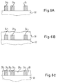
- Figures 6A-6F show cross-sections of a device construction useful for porous intralayer dielectrics.
- Figure 6A again shows patterned conductors 24 on a substrate 22 .
- a porous dielectric layer 28 is constructed to fill gaps between and cover conductors 24 , with the dried structure possibly resembling Figure 6B .
- Figure 6C shows the structure after removal of a top portion of porous layer 28 to preferably expose the tops of conductors 24 .
- the material removal may be accomplished, for example, by a controlled chemical etch, such as HF plasma etching, with concentrations and etch times strongly dependent on the dielectric porosity.
- the material removal may be done with a mechanical polisher, using, for example, an aqueous colloidal suspension of silica.
- a mechanical polisher using, for example, an aqueous colloidal suspension of silica.
- CVD chemical vapor deposition
- a dry-processed CVD layer which would primarily deposit near the top of the porous layer, may be preferable to spin-on glass (SOG), which may contain solvents capable of wetting the pores in porous layer 28 .
- SOG spin-on glass
- CVD is not particularly planarizing, and is a relatively slow method for forming a thick dielectric.
- Figure 6E illustrates how a non-porous dielectric 30 may be applied over conformal sublayer 56 , for example as an SOG oxide, to quickly complete a planarized interlayer dielectric.
- Figure 6F shows the structure after deposition and patterning of a photoresist mask 50 . This prepares the wafer for the etch of via 52 through layers 30 and 56 , as shown in Figure 6G .
- An advantage of this embodiment is that via 52 does not pass through porous dielectric 28 , which may be a difficult material to pattern precisely.
- Figure 6G shows a metal-filled via 32 and one of a second layer of patterned conductors 34 , electrically connected by metal-filled via 32 to one of patterned conductors 24 .
- This embodiment of the invention can provide excellent intralayer capacitance reduction, a good mechanical bond between porous and non-porous dielectrics, a straightforward construction technique with largely conventional via formation, and a planarized, non-porous interlayer dielectric with good mechanical and heat transfer characteristics.
- FIG 7 is included to illustrate an embodiment wherein porous dielectric layer 28 is isolated from conductors 24 by a relatively thin conformal passivation layer 54 , which may be formed, for example, of a CVD silicon dioxide. This layer may be advantageous in several embodiments. In an embodiment such as that of Figure 6 , layer 54 may be removed from the tops of conductors 24 during etchback of porous dielectric 28 .
- Figures 8A-8D illustrate an additional embodiment which includes dielectric spacers.
- conductors 24 are patterned with dielectric spacers 58 on top of them.
- the spacers are preferably formed of the same material used in non-porous layer 30 (shown on Figure 8D ). This may be accomplished by depositing a conducting layer, overlaying this with a dielectric layer of a material such as silicon dioxide, and patterning both with one mask.
- a porous dielectric layer 28 has been formed to preferably cover spacers 58 , as shown.
- Figure 8C shows the device after a top portion of porous dielectric 28 has been removed.
- FIG. 8C shows the device after non-porous dielectric 30 has been deposited over the structure to complete the interlayer dielectric.
- An advantage of this embodiment is that the addition of the spacers allows the removal of a top portion of the porous dielectric, without the possibility of removing a portion of the conductors. This structure may also result in lower crosstalk, as compared to the embodiment of Figure 6 .
Landscapes
- Internal Circuitry In Semiconductor Integrated Circuit Devices (AREA)
- Formation Of Insulating Films (AREA)
Applications Claiming Priority (2)
| Application Number | Priority Date | Filing Date | Title |
|---|---|---|---|
| US246432 | 1994-05-20 | ||
| US08/246,432 US5488015A (en) | 1994-05-20 | 1994-05-20 | Method of making an interconnect structure with an integrated low density dielectric |
Publications (2)
| Publication Number | Publication Date |
|---|---|
| EP0688052A2 true EP0688052A2 (de) | 1995-12-20 |
| EP0688052A3 EP0688052A3 (de) | 1996-08-28 |
Family
ID=22930666
Family Applications (1)
| Application Number | Title | Priority Date | Filing Date |
|---|---|---|---|
| EP95107519A Ceased EP0688052A3 (de) | 1994-05-20 | 1995-05-17 | Verbesserungen in der oder in Bezug auf die Herstellung einer Halbleiteranordnung |
Country Status (5)
| Country | Link |
|---|---|
| US (2) | US5488015A (de) |
| EP (1) | EP0688052A3 (de) |
| JP (1) | JPH07321206A (de) |
| KR (1) | KR950034792A (de) |
| TW (1) | TW296470B (de) |
Cited By (12)
| Publication number | Priority date | Publication date | Assignee | Title |
|---|---|---|---|---|
| WO2000013222A1 (en) * | 1998-08-27 | 2000-03-09 | Alliedsignal Inc. | Silane-based nanoporous silica thin films |
| EP0860879A3 (de) * | 1997-02-20 | 2000-05-24 | Nec Corporation | Mehrlagenverbindung in einer Halbleiteranordnung und Herstellungsverfahren dafür |
| WO2000044036A1 (en) * | 1999-01-26 | 2000-07-27 | Alliedsignal Inc. | Use of multifunctional si-based oligomer/polymer for the surface modification of nanoporous silica films |
| EP0881678A3 (de) * | 1997-05-28 | 2000-12-13 | Texas Instruments Incorporated | Verbesserungen in oder in Bezug zu porösen dielektrischen Strukturen |
| US6372666B1 (en) | 1998-08-31 | 2002-04-16 | Alliedsignal Inc. | Process for producing dielectric thin films |
| US6395651B1 (en) | 1998-07-07 | 2002-05-28 | Alliedsignal | Simplified process for producing nanoporous silica |
| US7500397B2 (en) | 2007-02-15 | 2009-03-10 | Air Products And Chemicals, Inc. | Activated chemical process for enhancing material properties of dielectric films |
| US7678712B2 (en) | 2005-03-22 | 2010-03-16 | Honeywell International, Inc. | Vapor phase treatment of dielectric materials |
| US7709371B2 (en) | 2003-01-25 | 2010-05-04 | Honeywell International Inc. | Repairing damage to low-k dielectric materials using silylating agents |
| US7858294B2 (en) | 2000-06-23 | 2010-12-28 | Honeywell International Inc. | Method to restore hydrophobicity in dielectric films and materials |
| US7915181B2 (en) | 2003-01-25 | 2011-03-29 | Honeywell International Inc. | Repair and restoration of damaged dielectric materials and films |
| US7915159B2 (en) | 2004-09-15 | 2011-03-29 | Honeywell International Inc. | Treating agent materials |
Families Citing this family (96)
| Publication number | Priority date | Publication date | Assignee | Title |
|---|---|---|---|---|
| JPH08148280A (ja) * | 1994-04-14 | 1996-06-07 | Toshiba Corp | 半導体装置およびその製造方法 |
| US5461003A (en) * | 1994-05-27 | 1995-10-24 | Texas Instruments Incorporated | Multilevel interconnect structure with air gaps formed between metal leads |
| JPH0845936A (ja) * | 1994-05-31 | 1996-02-16 | Texas Instr Inc <Ti> | ダミーリードを用いた高速lsi半導体装置およびその信頼性改善方法 |
| US5504042A (en) * | 1994-06-23 | 1996-04-02 | Texas Instruments Incorporated | Porous dielectric material with improved pore surface properties for electronics applications |
| US5472913A (en) * | 1994-08-05 | 1995-12-05 | Texas Instruments Incorporated | Method of fabricating porous dielectric material with a passivation layer for electronics applications |
| US5658832A (en) * | 1994-10-17 | 1997-08-19 | Regents Of The University Of California | Method of forming a spacer for field emission flat panel displays |
| US5627082A (en) * | 1995-03-29 | 1997-05-06 | Texas Instruments Incorporated | High thermal resistance backfill material for hybrid UFPA's |
| JPH0936226A (ja) * | 1995-07-18 | 1997-02-07 | Nec Corp | 半導体装置およびその製造方法 |
| US5942802A (en) | 1995-10-09 | 1999-08-24 | Matsushita Electric Industrial Co., Ltd. | Semiconductor device and method of producing the same |
| JP2836542B2 (ja) * | 1995-10-17 | 1998-12-14 | 日本電気株式会社 | 半導体装置の製造方法 |
| US5807607A (en) * | 1995-11-16 | 1998-09-15 | Texas Instruments Incorporated | Polyol-based method for forming thin film aerogels on semiconductor substrates |
| US5753305A (en) * | 1995-11-16 | 1998-05-19 | Texas Instruments Incorporated | Rapid aging technique for aerogel thin films |
| US5736425A (en) * | 1995-11-16 | 1998-04-07 | Texas Instruments Incorporated | Glycol-based method for forming a thin-film nanoporous dielectric |
| US6037277A (en) * | 1995-11-16 | 2000-03-14 | Texas Instruments Incorporated | Limited-volume apparatus and method for forming thin film aerogels on semiconductor substrates |
| US6130152A (en) | 1995-11-16 | 2000-10-10 | Texas Instruments Incorporated | Aerogel thin film formation from multi-solvent systems |
| US6380105B1 (en) | 1996-11-14 | 2002-04-30 | Texas Instruments Incorporated | Low volatility solvent-based method for forming thin film nanoporous aerogels on semiconductor substrates |
| US6319852B1 (en) | 1995-11-16 | 2001-11-20 | Texas Instruments Incorporated | Nanoporous dielectric thin film formation using a post-deposition catalyst |
| US6063714A (en) * | 1995-11-16 | 2000-05-16 | Texas Instruments Incorporated | Nanoporous dielectric thin film surface modification |
| US5861342A (en) * | 1995-12-26 | 1999-01-19 | Vlsi Technology, Inc. | Optimized structures for dummy fill mask design |
| US5618757A (en) * | 1996-01-30 | 1997-04-08 | Vlsi Technology, Inc. | Method for improving the manufacturability of the spin-on glass etchback process |
| US5639697A (en) * | 1996-01-30 | 1997-06-17 | Vlsi Technology, Inc. | Dummy underlayers for improvement in removal rate consistency during chemical mechanical polishing |
| US5783488A (en) * | 1996-01-31 | 1998-07-21 | Vlsi Technology, Inc. | Optimized underlayer structures for maintaining chemical mechanical polishing removal rates |
| JP2773729B2 (ja) * | 1996-02-29 | 1998-07-09 | 日本電気株式会社 | 半導体装置の製造方法 |
| US5965202A (en) * | 1996-05-02 | 1999-10-12 | Lucent Technologies, Inc. | Hybrid inorganic-organic composite for use as an interlayer dielectric |
| US6376330B1 (en) * | 1996-06-05 | 2002-04-23 | Advanced Micro Devices, Inc. | Dielectric having an air gap formed between closely spaced interconnect lines |
| US5814555A (en) | 1996-06-05 | 1998-09-29 | Advanced Micro Devices, Inc. | Interlevel dielectric with air gaps to lessen capacitive coupling |
| US6049132A (en) * | 1996-07-12 | 2000-04-11 | Kawasaki Steel Corporation | Multiple metallization structure for a reflection type liquid crystal display |
| US6040628A (en) * | 1996-12-19 | 2000-03-21 | Intel Corporation | Interconnect structure using a combination of hard dielectric and polymer as interlayer dielectrics |
| US6303464B1 (en) | 1996-12-30 | 2001-10-16 | Intel Corporation | Method and structure for reducing interconnect system capacitance through enclosed voids in a dielectric layer |
| US5854125A (en) * | 1997-02-24 | 1998-12-29 | Vlsi Technology, Inc. | Dummy fill patterns to improve interconnect planarity |
| US5981374A (en) * | 1997-04-29 | 1999-11-09 | International Business Machines Corporation | Sub-half-micron multi-level interconnection structure and process thereof |
| US6351039B1 (en) * | 1997-05-28 | 2002-02-26 | Texas Instruments Incorporated | Integrated circuit dielectric and method |
| US6008540A (en) * | 1997-05-28 | 1999-12-28 | Texas Instruments Incorporated | Integrated circuit dielectric and method |
| US6437441B1 (en) | 1997-07-10 | 2002-08-20 | Kawasaki Microelectronics, Inc. | Wiring structure of a semiconductor integrated circuit and a method of forming the wiring structure |
| US6090711A (en) * | 1997-09-30 | 2000-07-18 | Semitool, Inc. | Methods for controlling semiconductor workpiece surface exposure to processing liquids |
| US6858526B2 (en) | 1998-07-14 | 2005-02-22 | Micron Technology, Inc. | Methods of forming materials between conductive electrical components, and insulating materials |
| US6251470B1 (en) * | 1997-10-09 | 2001-06-26 | Micron Technology, Inc. | Methods of forming insulating materials, and methods of forming insulating materials around a conductive component |
| US6333556B1 (en) | 1997-10-09 | 2001-12-25 | Micron Technology, Inc. | Insulating materials |
| US6350704B1 (en) | 1997-10-14 | 2002-02-26 | Micron Technology Inc. | Porous silicon oxycarbide integrated circuit insulator |
| US6248168B1 (en) * | 1997-12-15 | 2001-06-19 | Tokyo Electron Limited | Spin coating apparatus including aging unit and solvent replacement unit |
| US6340435B1 (en) | 1998-02-11 | 2002-01-22 | Applied Materials, Inc. | Integrated low K dielectrics and etch stops |
| US6303523B2 (en) * | 1998-02-11 | 2001-10-16 | Applied Materials, Inc. | Plasma processes for depositing low dielectric constant films |
| US6054379A (en) * | 1998-02-11 | 2000-04-25 | Applied Materials, Inc. | Method of depositing a low k dielectric with organo silane |
| US6287990B1 (en) | 1998-02-11 | 2001-09-11 | Applied Materials, Inc. | CVD plasma assisted low dielectric constant films |
| US6660656B2 (en) | 1998-02-11 | 2003-12-09 | Applied Materials Inc. | Plasma processes for depositing low dielectric constant films |
| US6627532B1 (en) * | 1998-02-11 | 2003-09-30 | Applied Materials, Inc. | Method of decreasing the K value in SiOC layer deposited by chemical vapor deposition |
| JP3571522B2 (ja) | 1998-02-12 | 2004-09-29 | 松下電器産業株式会社 | 多孔質膜の形成方法及び多孔質膜の形成材料 |
| US6160316A (en) * | 1998-03-04 | 2000-12-12 | Advanced Micro Devices, Inc. | Integrated circuit utilizing an air gap to reduce capacitance between adjacent metal linewidths |
| US6149987A (en) * | 1998-04-07 | 2000-11-21 | Applied Materials, Inc. | Method for depositing low dielectric constant oxide films |
| US6420278B1 (en) * | 1998-06-12 | 2002-07-16 | Advanced Micro Devices, Inc. | Method for improving the dielectric constant of silicon-based semiconductor materials |
| US6054206A (en) * | 1998-06-22 | 2000-04-25 | Novellus Systems, Inc. | Chemical vapor deposition of low density silicon dioxide films |
| US6140221A (en) * | 1998-07-29 | 2000-10-31 | Philips Electronics North America Corp. | Method for forming vias through porous dielectric material and devices formed thereby |
| US6133619A (en) * | 1998-08-31 | 2000-10-17 | Advanced Micro Devices, Inc. | Reduction of silicon oxynitride film delamination in integrated circuit inter-level dielectrics |
| US6124640A (en) * | 1998-08-31 | 2000-09-26 | Advanced Micro Devices, Inc. | Scalable and reliable integrated circuit inter-level dielectric |
| US6187672B1 (en) | 1998-09-22 | 2001-02-13 | Conexant Systems, Inc. | Interconnect with low dielectric constant insulators for semiconductor integrated circuit manufacturing |
| TW429576B (en) * | 1998-10-14 | 2001-04-11 | United Microelectronics Corp | Manufacturing method for metal interconnect |
| US6265301B1 (en) * | 1999-05-12 | 2001-07-24 | Taiwan Semiconductor Manufacturing Company | Method of forming metal interconnect structures and metal via structures using photolithographic and electroplating or electro-less plating procedures |
| US6306754B1 (en) * | 1999-06-29 | 2001-10-23 | Micron Technology, Inc. | Method for forming wiring with extremely low parasitic capacitance |
| US6350679B1 (en) | 1999-08-03 | 2002-02-26 | Micron Technology, Inc. | Methods of providing an interlevel dielectric layer intermediate different elevation conductive metal layers in the fabrication of integrated circuitry |
| US6395631B1 (en) | 1999-08-04 | 2002-05-28 | Chartered Semiconductor Manufacturing Ltd. | Low dielectric constant dielectric layer fabrication method employing hard mask layer delamination |
| US6709968B1 (en) * | 2000-08-16 | 2004-03-23 | Micron Technology, Inc. | Microelectronic device with package with conductive elements and associated method of manufacture |
| US7335965B2 (en) * | 1999-08-25 | 2008-02-26 | Micron Technology, Inc. | Packaging of electronic chips with air-bridge structures |
| US6670719B2 (en) | 1999-08-25 | 2003-12-30 | Micron Technology, Inc. | Microelectronic device package filled with liquid or pressurized gas and associated method of manufacture |
| US7276788B1 (en) | 1999-08-25 | 2007-10-02 | Micron Technology, Inc. | Hydrophobic foamed insulators for high density circuits |
| US6875687B1 (en) | 1999-10-18 | 2005-04-05 | Applied Materials, Inc. | Capping layer for extreme low dielectric constant films |
| EP1094506A3 (de) | 1999-10-18 | 2004-03-03 | Applied Materials, Inc. | Schutzschicht für Filme mit besonders kleiner Dielektrizitätskonstante |
| EP1124252A2 (de) * | 2000-02-10 | 2001-08-16 | Applied Materials, Inc. | Verfahren und Vorrichtung zur Verarbeitung von Substraten |
| US6677209B2 (en) | 2000-02-14 | 2004-01-13 | Micron Technology, Inc. | Low dielectric constant STI with SOI devices |
| US6413827B2 (en) | 2000-02-14 | 2002-07-02 | Paul A. Farrar | Low dielectric constant shallow trench isolation |
| US6890847B1 (en) * | 2000-02-22 | 2005-05-10 | Micron Technology, Inc. | Polynorbornene foam insulation for integrated circuits |
| US7265062B2 (en) * | 2000-04-04 | 2007-09-04 | Applied Materials, Inc. | Ionic additives for extreme low dielectric constant chemical formulations |
| US6576568B2 (en) | 2000-04-04 | 2003-06-10 | Applied Materials, Inc. | Ionic additives for extreme low dielectric constant chemical formulations |
| US6753270B1 (en) | 2000-08-04 | 2004-06-22 | Applied Materials Inc. | Process for depositing a porous, low dielectric constant silicon oxide film |
| DE10059935A1 (de) * | 2000-11-28 | 2002-06-06 | Infineon Technologies Ag | Dicht gepackte Halbleiterstruktur und Verfahren zum Herstellen einer solchen |
| US7077859B2 (en) | 2000-12-22 | 2006-07-18 | Avantec Vascular Corporation | Apparatus and methods for variably controlled substance delivery from implanted prostheses |
| TW476135B (en) * | 2001-01-09 | 2002-02-11 | United Microelectronics Corp | Manufacture of semiconductor with air gap |
| US6627534B1 (en) * | 2001-02-05 | 2003-09-30 | Henry F. Lee | Semiconductor fabrication process and structure with minimal capacitive coupling between conductors |
| US6709721B2 (en) | 2001-03-28 | 2004-03-23 | Applied Materials Inc. | Purge heater design and process development for the improvement of low k film properties |
| US7142256B2 (en) * | 2001-08-28 | 2006-11-28 | Crest Health Care | Television control device |
| US7196422B2 (en) | 2001-12-14 | 2007-03-27 | Intel Corporation | Low-dielectric constant structure with a multilayer stack of thin films with pores |
| TW548327B (en) * | 2002-06-25 | 2003-08-21 | Ind Tech Res Inst | SOG materials for anodic bonding spacer |
| KR100478480B1 (ko) * | 2002-07-30 | 2005-03-28 | 동부아남반도체 주식회사 | 반도체 소자 및 그 제조 방법 |
| US7153754B2 (en) * | 2002-08-29 | 2006-12-26 | Micron Technology, Inc. | Methods for forming porous insulators from “void” creating materials and structures and semiconductor devices including same |
| TW574448B (en) * | 2002-09-24 | 2004-02-01 | Au Optronics Corp | Method for fabricating a polysilicon layer |
| JP3793143B2 (ja) * | 2002-11-28 | 2006-07-05 | 株式会社シマノ | 自転車用電子制御装置 |
| US7192892B2 (en) | 2003-03-04 | 2007-03-20 | Micron Technology, Inc. | Atomic layer deposited dielectric layers |
| US20050137882A1 (en) * | 2003-12-17 | 2005-06-23 | Cameron Don T. | Method for authenticating goods |
| US20050183740A1 (en) * | 2004-02-19 | 2005-08-25 | Fulton John L. | Process and apparatus for removing residues from semiconductor substrates |
| US7927948B2 (en) | 2005-07-20 | 2011-04-19 | Micron Technology, Inc. | Devices with nanocrystals and methods of formation |
| US20090026924A1 (en) * | 2007-07-23 | 2009-01-29 | Leung Roger Y | Methods of making low-refractive index and/or low-k organosilicate coatings |
| AU2009227882B2 (en) * | 2008-10-27 | 2015-06-25 | Hoya Corporation | Process for producing polarizing element |
| US8969132B2 (en) | 2010-09-20 | 2015-03-03 | Nuvotronics, Llc | Device package and methods for the fabrication thereof |
| US9337152B2 (en) | 2013-03-15 | 2016-05-10 | Nuvotronics, Inc | Formulation for packaging an electronic device and assemblies made therefrom |
| US9437479B2 (en) * | 2013-11-19 | 2016-09-06 | Applied Materials, Inc. | Methods for forming an interconnect pattern on a substrate |
| US9613906B2 (en) * | 2014-06-23 | 2017-04-04 | GlobalFoundries, Inc. | Integrated circuits including modified liners and methods for fabricating the same |
| KR20230013712A (ko) | 2021-07-19 | 2023-01-27 | 삼성전자주식회사 | 반도체 장치 |
Citations (2)
| Publication number | Priority date | Publication date | Assignee | Title |
|---|---|---|---|---|
| US4652467A (en) | 1985-02-25 | 1987-03-24 | The United States Of America As Represented By The United States Department Of Energy | Inorganic-polymer-derived dielectric films |
| US4987101A (en) | 1988-12-16 | 1991-01-22 | International Business Machines Corporation | Method for providing improved insulation in VLSI and ULSI circuits |
Family Cites Families (24)
| Publication number | Priority date | Publication date | Assignee | Title |
|---|---|---|---|---|
| DE2357184A1 (de) * | 1973-11-16 | 1975-05-22 | Merck Patent Gmbh | Verfahren zur herstellung von organisch modifizierten siliciumdioxiden |
| US4141055A (en) * | 1977-04-27 | 1979-02-20 | Bell Telephone Laboratories, Incorporated | Crossover structure for microelectronic circuits |
| DE3345040A1 (de) * | 1983-12-13 | 1985-06-13 | Siemens AG, 1000 Berlin und 8000 München | Verfahren zur herstellung einer eingeebneten, die zwei metallisierungen trennenden anorganischen isolationsschicht unter verwendung von polyimid |
| US4619839A (en) * | 1984-12-12 | 1986-10-28 | Fairchild Camera & Instrument Corp. | Method of forming a dielectric layer on a semiconductor device |
| JPH0612790B2 (ja) * | 1987-02-24 | 1994-02-16 | 日本電気株式会社 | 半導体装置 |
| JPS6451625A (en) * | 1987-08-24 | 1989-02-27 | Fujitsu Ltd | Manufacture of semiconductor device |
| JPS6459815A (en) * | 1987-08-31 | 1989-03-07 | Hitachi Ltd | Formation of pattern |
| JPH063804B2 (ja) * | 1988-01-21 | 1994-01-12 | シャープ株式会社 | 半導体装置製造方法 |
| JPH01235254A (ja) * | 1988-03-15 | 1989-09-20 | Nec Corp | 半導体装置及びその製造方法 |
| US4885262A (en) * | 1989-03-08 | 1989-12-05 | Intel Corporation | Chemical modification of spin-on glass for improved performance in IC fabrication |
| US5270267A (en) * | 1989-05-31 | 1993-12-14 | Mitel Corporation | Curing and passivation of spin on glasses by a plasma process wherein an external polarization field is applied to the substrate |
| US5023208A (en) * | 1989-12-19 | 1991-06-11 | Orion Laboratories, Inc. | Sol-gel process for glass and ceramic articles |
| US5104828A (en) * | 1990-03-01 | 1992-04-14 | Intel Corporation | Method of planarizing a dielectric formed over a semiconductor substrate |
| JPH04174541A (ja) * | 1990-03-28 | 1992-06-22 | Nec Corp | 半導体集積回路及びその製造方法 |
| JP2550508B2 (ja) * | 1990-10-17 | 1996-11-06 | 三菱電機株式会社 | 半導体装置,およびその製造方法 |
| JPH0645327A (ja) * | 1991-01-09 | 1994-02-18 | Nec Corp | 半導体装置の製造方法 |
| JPH0782999B2 (ja) * | 1991-04-15 | 1995-09-06 | 株式会社半導体プロセス研究所 | 気相成長膜の形成方法、半導体製造装置、および半 導体装置 |
| KR950002948B1 (ko) * | 1991-10-10 | 1995-03-28 | 삼성전자 주식회사 | 반도체 장치의 금속층간 절연막 형성방법 |
| KR100220297B1 (ko) * | 1991-12-02 | 1999-09-15 | 김영환 | 다층금속 배선구조의 콘택제조방법 |
| JPH05283542A (ja) * | 1992-03-31 | 1993-10-29 | Mitsubishi Electric Corp | 半導体集積回路装置及びその製造方法 |
| JP3031796B2 (ja) * | 1992-07-31 | 2000-04-10 | 松下電器産業株式会社 | 薄膜形成方法及び半導体装置の製造方法 |
| JPH0684787A (ja) * | 1992-09-01 | 1994-03-25 | Fujitsu Ltd | 多層レジストのパターン形成方法 |
| KR0131439B1 (ko) * | 1992-11-24 | 1998-04-14 | 나카무라 타메아키 | 반도체장치 및 그 제조방법 |
| US5565384A (en) * | 1994-04-28 | 1996-10-15 | Texas Instruments Inc | Self-aligned via using low permittivity dielectric |
-
1994
- 1994-05-20 US US08/246,432 patent/US5488015A/en not_active Expired - Lifetime
-
1995
- 1995-05-17 EP EP95107519A patent/EP0688052A3/de not_active Ceased
- 1995-05-18 JP JP7120214A patent/JPH07321206A/ja active Pending
- 1995-05-19 KR KR1019950012540A patent/KR950034792A/ko not_active Ceased
- 1995-06-08 TW TW084105789A patent/TW296470B/zh not_active IP Right Cessation
-
1996
- 1996-11-18 US US08/751,901 patent/US5747880A/en not_active Expired - Lifetime
Patent Citations (2)
| Publication number | Priority date | Publication date | Assignee | Title |
|---|---|---|---|---|
| US4652467A (en) | 1985-02-25 | 1987-03-24 | The United States Of America As Represented By The United States Department Of Energy | Inorganic-polymer-derived dielectric films |
| US4987101A (en) | 1988-12-16 | 1991-01-22 | International Business Machines Corporation | Method for providing improved insulation in VLSI and ULSI circuits |
Cited By (18)
| Publication number | Priority date | Publication date | Assignee | Title |
|---|---|---|---|---|
| EP0860879A3 (de) * | 1997-02-20 | 2000-05-24 | Nec Corporation | Mehrlagenverbindung in einer Halbleiteranordnung und Herstellungsverfahren dafür |
| EP0881678A3 (de) * | 1997-05-28 | 2000-12-13 | Texas Instruments Incorporated | Verbesserungen in oder in Bezug zu porösen dielektrischen Strukturen |
| WO2000002233A3 (en) * | 1998-07-07 | 2003-04-17 | Allied Signal Inc | Simplified process for producing nanoporous silica |
| US6395651B1 (en) | 1998-07-07 | 2002-05-28 | Alliedsignal | Simplified process for producing nanoporous silica |
| US6495906B2 (en) | 1998-07-07 | 2002-12-17 | Alliedsignal Inc. | Simplified process for producing nanoporous silica |
| KR100682614B1 (ko) * | 1998-08-27 | 2007-02-15 | 알라이드시그날 인코포레이티드 | 실란계 나노 다공성 실리카 박막 및 그 제조방법 |
| WO2000013222A1 (en) * | 1998-08-27 | 2000-03-09 | Alliedsignal Inc. | Silane-based nanoporous silica thin films |
| US6559071B2 (en) | 1998-08-31 | 2003-05-06 | Alliedsignal Inc. | Process for producing dielectric thin films |
| US6372666B1 (en) | 1998-08-31 | 2002-04-16 | Alliedsignal Inc. | Process for producing dielectric thin films |
| US6770572B1 (en) | 1999-01-26 | 2004-08-03 | Alliedsignal Inc. | Use of multifunctional si-based oligomer/polymer for the surface modification of nanoporous silica films |
| WO2000044036A1 (en) * | 1999-01-26 | 2000-07-27 | Alliedsignal Inc. | Use of multifunctional si-based oligomer/polymer for the surface modification of nanoporous silica films |
| US7858294B2 (en) | 2000-06-23 | 2010-12-28 | Honeywell International Inc. | Method to restore hydrophobicity in dielectric films and materials |
| US8440388B2 (en) | 2000-06-23 | 2013-05-14 | Honeywell International Inc. | Method to restore hydrophobicity in dielectric films and materials |
| US7709371B2 (en) | 2003-01-25 | 2010-05-04 | Honeywell International Inc. | Repairing damage to low-k dielectric materials using silylating agents |
| US7915181B2 (en) | 2003-01-25 | 2011-03-29 | Honeywell International Inc. | Repair and restoration of damaged dielectric materials and films |
| US7915159B2 (en) | 2004-09-15 | 2011-03-29 | Honeywell International Inc. | Treating agent materials |
| US7678712B2 (en) | 2005-03-22 | 2010-03-16 | Honeywell International, Inc. | Vapor phase treatment of dielectric materials |
| US7500397B2 (en) | 2007-02-15 | 2009-03-10 | Air Products And Chemicals, Inc. | Activated chemical process for enhancing material properties of dielectric films |
Also Published As
| Publication number | Publication date |
|---|---|
| US5488015A (en) | 1996-01-30 |
| JPH07321206A (ja) | 1995-12-08 |
| KR950034792A (ko) | 1995-12-28 |
| EP0688052A3 (de) | 1996-08-28 |
| US5747880A (en) | 1998-05-05 |
| TW296470B (de) | 1997-01-21 |
Similar Documents
| Publication | Publication Date | Title |
|---|---|---|
| US5747880A (en) | Interconnect structure with an integrated low density dielectric | |
| US5789819A (en) | Low dielectric constant material for electronics applications | |
| US5494858A (en) | Method for forming porous composites as a low dielectric constant layer with varying porosity distribution electronics applications | |
| US5472913A (en) | Method of fabricating porous dielectric material with a passivation layer for electronics applications | |
| EP0689235B1 (de) | Poröses dielektrisches Material mit verbesserten Porenoberflächen für elektronische Anwendungen | |
| US5750415A (en) | Low dielectric constant layers via immiscible sol-gel processing | |
| JP4014234B2 (ja) | 半導体デバイス中に線間容量の低減化された相互接続線を作製する方法 | |
| US5668398A (en) | Multilevel interconnect structure with air gaps formed between metal leads | |
| US6492259B2 (en) | Process for making a planar integrated circuit interconnect | |
| JPH10178006A (ja) | 集積回路誘電体 | |
| JPH113888A (ja) | 集積回路誘電体及び方法 | |
| TW523867B (en) | Deliberate void in innerlayer dielectric gapfill to reduce dielectric constant | |
| JP2000091330A (ja) | 集積回路誘電体及びその製法 | |
| CN115565933B (zh) | 介电结构、制备方法、以及半导体器件 | |
| KR20070019172A (ko) | 다마신 공정의 방법 | |
| US7674390B2 (en) | Zeolite—sol gel nano-composite low k dielectric |
Legal Events
| Date | Code | Title | Description |
|---|---|---|---|
| PUAI | Public reference made under article 153(3) epc to a published international application that has entered the european phase |
Free format text: ORIGINAL CODE: 0009012 |
|
| AK | Designated contracting states |
Kind code of ref document: A2 Designated state(s): DE FR GB IT NL |
|
| PUAL | Search report despatched |
Free format text: ORIGINAL CODE: 0009013 |
|
| AK | Designated contracting states |
Kind code of ref document: A3 Designated state(s): DE FR GB IT NL |
|
| 17P | Request for examination filed |
Effective date: 19970228 |
|
| 17Q | First examination report despatched |
Effective date: 19980728 |
|
| GRAG | Despatch of communication of intention to grant |
Free format text: ORIGINAL CODE: EPIDOS AGRA |
|
| RIC1 | Information provided on ipc code assigned before grant |
Free format text: 7H 01L 23/522 A, 7H 01L 23/532 B |
|
| RTI1 | Title (correction) |
Free format text: METHOD OFMAKING A MULTILAYER WIRING STRUCTURE WITH POROUS DIELECTRIC MATERIAL |
|
| STAA | Information on the status of an ep patent application or granted ep patent |
Free format text: STATUS: THE APPLICATION HAS BEEN REFUSED |
|
| 18R | Application refused |
Effective date: 20011027 |