EP0689085A2 - Dispositif d'affichage et son procédé de fabrication - Google Patents
Dispositif d'affichage et son procédé de fabrication Download PDFInfo
- Publication number
- EP0689085A2 EP0689085A2 EP95304240A EP95304240A EP0689085A2 EP 0689085 A2 EP0689085 A2 EP 0689085A2 EP 95304240 A EP95304240 A EP 95304240A EP 95304240 A EP95304240 A EP 95304240A EP 0689085 A2 EP0689085 A2 EP 0689085A2
- Authority
- EP
- European Patent Office
- Prior art keywords
- film
- display device
- substrate
- liquid crystal
- active matrix
- Prior art date
- Legal status (The legal status is an assumption and is not a legal conclusion. Google has not performed a legal analysis and makes no representation as to the accuracy of the status listed.)
- Granted
Links
- 238000000034 method Methods 0.000 title claims description 73
- 238000004519 manufacturing process Methods 0.000 title claims description 16
- 239000010408 film Substances 0.000 claims abstract description 318
- 239000000758 substrate Substances 0.000 claims abstract description 161
- 239000004973 liquid crystal related substance Substances 0.000 claims abstract description 100
- 239000010410 layer Substances 0.000 claims abstract description 69
- 229910021420 polycrystalline silicon Inorganic materials 0.000 claims abstract description 64
- 239000004065 semiconductor Substances 0.000 claims abstract description 60
- 239000011159 matrix material Substances 0.000 claims abstract description 51
- 239000010409 thin film Substances 0.000 claims abstract description 21
- 229910052581 Si3N4 Inorganic materials 0.000 claims description 68
- HQVNEWCFYHHQES-UHFFFAOYSA-N silicon nitride Chemical compound N12[Si]34N5[Si]62N3[Si]51N64 HQVNEWCFYHHQES-UHFFFAOYSA-N 0.000 claims description 68
- 230000008569 process Effects 0.000 claims description 64
- UFHFLCQGNIYNRP-UHFFFAOYSA-N Hydrogen Chemical compound [H][H] UFHFLCQGNIYNRP-UHFFFAOYSA-N 0.000 claims description 45
- 239000001257 hydrogen Substances 0.000 claims description 44
- 229910052739 hydrogen Inorganic materials 0.000 claims description 44
- XUIMIQQOPSSXEZ-UHFFFAOYSA-N Silicon Chemical compound [Si] XUIMIQQOPSSXEZ-UHFFFAOYSA-N 0.000 claims description 29
- 229910052710 silicon Inorganic materials 0.000 claims description 25
- 239000010703 silicon Substances 0.000 claims description 25
- 238000005268 plasma chemical vapour deposition Methods 0.000 claims description 20
- 238000009792 diffusion process Methods 0.000 claims description 19
- VYPSYNLAJGMNEJ-UHFFFAOYSA-N silicon dioxide Inorganic materials O=[Si]=O VYPSYNLAJGMNEJ-UHFFFAOYSA-N 0.000 claims description 18
- 230000002093 peripheral effect Effects 0.000 claims description 14
- 230000005540 biological transmission Effects 0.000 claims description 12
- 150000004767 nitrides Chemical class 0.000 claims description 11
- 229910021421 monocrystalline silicon Inorganic materials 0.000 claims description 8
- 239000010453 quartz Substances 0.000 claims description 8
- 230000003287 optical effect Effects 0.000 claims description 6
- 239000011521 glass Substances 0.000 claims description 5
- 150000002431 hydrogen Chemical class 0.000 claims description 3
- 238000003384 imaging method Methods 0.000 claims 1
- 230000002401 inhibitory effect Effects 0.000 claims 1
- 229920005591 polysilicon Polymers 0.000 description 26
- 229910052751 metal Inorganic materials 0.000 description 19
- 239000002184 metal Substances 0.000 description 19
- 239000007789 gas Substances 0.000 description 15
- 239000005360 phosphosilicate glass Substances 0.000 description 14
- 239000000463 material Substances 0.000 description 13
- 229910052814 silicon oxide Inorganic materials 0.000 description 13
- 239000011229 interlayer Substances 0.000 description 12
- 238000000137 annealing Methods 0.000 description 11
- 238000005530 etching Methods 0.000 description 11
- BLRPTPMANUNPDV-UHFFFAOYSA-N Silane Chemical compound [SiH4] BLRPTPMANUNPDV-UHFFFAOYSA-N 0.000 description 9
- 230000005684 electric field Effects 0.000 description 9
- 238000005984 hydrogenation reaction Methods 0.000 description 9
- 229910000077 silane Inorganic materials 0.000 description 9
- 239000012528 membrane Substances 0.000 description 8
- 229910052782 aluminium Inorganic materials 0.000 description 7
- 239000005262 ferroelectric liquid crystals (FLCs) Substances 0.000 description 7
- GQPLMRYTRLFLPF-UHFFFAOYSA-N Nitrous Oxide Chemical compound [O-][N+]#N GQPLMRYTRLFLPF-UHFFFAOYSA-N 0.000 description 6
- XAGFODPZIPBFFR-UHFFFAOYSA-N aluminium Chemical compound [Al] XAGFODPZIPBFFR-UHFFFAOYSA-N 0.000 description 6
- 230000000694 effects Effects 0.000 description 6
- 238000010438 heat treatment Methods 0.000 description 6
- 125000004435 hydrogen atom Chemical group [H]* 0.000 description 6
- 230000009467 reduction Effects 0.000 description 6
- 238000002230 thermal chemical vapour deposition Methods 0.000 description 6
- 238000000151 deposition Methods 0.000 description 5
- ATJFFYVFTNAWJD-UHFFFAOYSA-N Tin Chemical compound [Sn] ATJFFYVFTNAWJD-UHFFFAOYSA-N 0.000 description 4
- 230000006872 improvement Effects 0.000 description 4
- 238000000059 patterning Methods 0.000 description 4
- 239000000049 pigment Substances 0.000 description 4
- 230000000630 rising effect Effects 0.000 description 4
- IJGRMHOSHXDMSA-UHFFFAOYSA-N Atomic nitrogen Chemical compound N#N IJGRMHOSHXDMSA-UHFFFAOYSA-N 0.000 description 3
- XYFCBTPGUUZFHI-UHFFFAOYSA-N Phosphine Chemical compound P XYFCBTPGUUZFHI-UHFFFAOYSA-N 0.000 description 3
- 230000008021 deposition Effects 0.000 description 3
- 239000000203 mixture Substances 0.000 description 3
- 235000013842 nitrous oxide Nutrition 0.000 description 3
- QGZKDVFQNNGYKY-UHFFFAOYSA-N Ammonia Chemical compound N QGZKDVFQNNGYKY-UHFFFAOYSA-N 0.000 description 2
- 229910021417 amorphous silicon Inorganic materials 0.000 description 2
- 229910052804 chromium Inorganic materials 0.000 description 2
- 238000010586 diagram Methods 0.000 description 2
- 239000000975 dye Substances 0.000 description 2
- 239000007772 electrode material Substances 0.000 description 2
- 239000012535 impurity Substances 0.000 description 2
- 150000002500 ions Chemical class 0.000 description 2
- 230000003071 parasitic effect Effects 0.000 description 2
- -1 phosphor ions Chemical class 0.000 description 2
- 229910000073 phosphorus hydride Inorganic materials 0.000 description 2
- 229920001721 polyimide Polymers 0.000 description 2
- 230000002035 prolonged effect Effects 0.000 description 2
- 238000000926 separation method Methods 0.000 description 2
- 125000006850 spacer group Chemical group 0.000 description 2
- 229910052715 tantalum Inorganic materials 0.000 description 2
- 230000037303 wrinkles Effects 0.000 description 2
- 229910000838 Al alloy Inorganic materials 0.000 description 1
- 229910000789 Aluminium-silicon alloy Inorganic materials 0.000 description 1
- 241000293849 Cordylanthus Species 0.000 description 1
- MYMOFIZGZYHOMD-UHFFFAOYSA-N Dioxygen Chemical compound O=O MYMOFIZGZYHOMD-UHFFFAOYSA-N 0.000 description 1
- KRHYYFGTRYWZRS-UHFFFAOYSA-N Fluorane Chemical compound F KRHYYFGTRYWZRS-UHFFFAOYSA-N 0.000 description 1
- 229910004166 TaN Inorganic materials 0.000 description 1
- 230000001133 acceleration Effects 0.000 description 1
- 230000009471 action Effects 0.000 description 1
- 230000002411 adverse Effects 0.000 description 1
- PNEYBMLMFCGWSK-UHFFFAOYSA-N aluminium oxide Inorganic materials [O-2].[O-2].[O-2].[Al+3].[Al+3] PNEYBMLMFCGWSK-UHFFFAOYSA-N 0.000 description 1
- 229910052785 arsenic Inorganic materials 0.000 description 1
- RQNWIZPPADIBDY-UHFFFAOYSA-N arsenic atom Chemical compound [As] RQNWIZPPADIBDY-UHFFFAOYSA-N 0.000 description 1
- 229910052802 copper Inorganic materials 0.000 description 1
- 229910052593 corundum Inorganic materials 0.000 description 1
- 238000000354 decomposition reaction Methods 0.000 description 1
- 230000007547 defect Effects 0.000 description 1
- 229910001873 dinitrogen Inorganic materials 0.000 description 1
- 229910001882 dioxygen Inorganic materials 0.000 description 1
- 230000009977 dual effect Effects 0.000 description 1
- 230000005611 electricity Effects 0.000 description 1
- 229960002050 hydrofluoric acid Drugs 0.000 description 1
- 238000002513 implantation Methods 0.000 description 1
- 239000011261 inert gas Substances 0.000 description 1
- 238000001755 magnetron sputter deposition Methods 0.000 description 1
- 230000008018 melting Effects 0.000 description 1
- 238000002844 melting Methods 0.000 description 1
- 229910052750 molybdenum Inorganic materials 0.000 description 1
- 238000005121 nitriding Methods 0.000 description 1
- 229910052757 nitrogen Inorganic materials 0.000 description 1
- 230000003647 oxidation Effects 0.000 description 1
- 238000007254 oxidation reaction Methods 0.000 description 1
- 230000001590 oxidative effect Effects 0.000 description 1
- 125000004430 oxygen atom Chemical group O* 0.000 description 1
- 238000002161 passivation Methods 0.000 description 1
- 239000005368 silicate glass Substances 0.000 description 1
- 229910021332 silicide Inorganic materials 0.000 description 1
- FVBUAEGBCNSCDD-UHFFFAOYSA-N silicide(4-) Chemical compound [Si-4] FVBUAEGBCNSCDD-UHFFFAOYSA-N 0.000 description 1
- 230000000087 stabilizing effect Effects 0.000 description 1
- 229910052719 titanium Inorganic materials 0.000 description 1
- 229910052721 tungsten Inorganic materials 0.000 description 1
- 229910001845 yogo sapphire Inorganic materials 0.000 description 1
Images







Classifications
-
- G—PHYSICS
- G02—OPTICS
- G02F—OPTICAL DEVICES OR ARRANGEMENTS FOR THE CONTROL OF LIGHT BY MODIFICATION OF THE OPTICAL PROPERTIES OF THE MEDIA OF THE ELEMENTS INVOLVED THEREIN; NON-LINEAR OPTICS; FREQUENCY-CHANGING OF LIGHT; OPTICAL LOGIC ELEMENTS; OPTICAL ANALOGUE/DIGITAL CONVERTERS
- G02F1/00—Devices or arrangements for the control of the intensity, colour, phase, polarisation or direction of light arriving from an independent light source, e.g. switching, gating or modulating; Non-linear optics
- G02F1/01—Devices or arrangements for the control of the intensity, colour, phase, polarisation or direction of light arriving from an independent light source, e.g. switching, gating or modulating; Non-linear optics for the control of the intensity, phase, polarisation or colour
- G02F1/13—Devices or arrangements for the control of the intensity, colour, phase, polarisation or direction of light arriving from an independent light source, e.g. switching, gating or modulating; Non-linear optics for the control of the intensity, phase, polarisation or colour based on liquid crystals, e.g. single liquid crystal display cells
- G02F1/133—Constructional arrangements; Operation of liquid crystal cells; Circuit arrangements
- G02F1/1333—Constructional arrangements; Manufacturing methods
- G02F1/1345—Conductors connecting electrodes to cell terminals
- G02F1/13454—Drivers integrated on the active matrix substrate
-
- H—ELECTRICITY
- H10—SEMICONDUCTOR DEVICES; ELECTRIC SOLID-STATE DEVICES NOT OTHERWISE PROVIDED FOR
- H10D—INORGANIC ELECTRIC SEMICONDUCTOR DEVICES
- H10D86/00—Integrated devices formed in or on insulating or conducting substrates, e.g. formed in silicon-on-insulator [SOI] substrates or on stainless steel or glass substrates
-
- G—PHYSICS
- G02—OPTICS
- G02F—OPTICAL DEVICES OR ARRANGEMENTS FOR THE CONTROL OF LIGHT BY MODIFICATION OF THE OPTICAL PROPERTIES OF THE MEDIA OF THE ELEMENTS INVOLVED THEREIN; NON-LINEAR OPTICS; FREQUENCY-CHANGING OF LIGHT; OPTICAL LOGIC ELEMENTS; OPTICAL ANALOGUE/DIGITAL CONVERTERS
- G02F1/00—Devices or arrangements for the control of the intensity, colour, phase, polarisation or direction of light arriving from an independent light source, e.g. switching, gating or modulating; Non-linear optics
- G02F1/01—Devices or arrangements for the control of the intensity, colour, phase, polarisation or direction of light arriving from an independent light source, e.g. switching, gating or modulating; Non-linear optics for the control of the intensity, phase, polarisation or colour
- G02F1/13—Devices or arrangements for the control of the intensity, colour, phase, polarisation or direction of light arriving from an independent light source, e.g. switching, gating or modulating; Non-linear optics for the control of the intensity, phase, polarisation or colour based on liquid crystals, e.g. single liquid crystal display cells
- G02F1/133—Constructional arrangements; Operation of liquid crystal cells; Circuit arrangements
- G02F1/136—Liquid crystal cells structurally associated with a semi-conducting layer or substrate, e.g. cells forming part of an integrated circuit
- G02F1/1362—Active matrix addressed cells
- G02F1/136277—Active matrix addressed cells formed on a semiconductor substrate, e.g. of silicon
- G02F1/136281—Active matrix addressed cells formed on a semiconductor substrate, e.g. of silicon having a transmissive semiconductor substrate
-
- G—PHYSICS
- G02—OPTICS
- G02F—OPTICAL DEVICES OR ARRANGEMENTS FOR THE CONTROL OF LIGHT BY MODIFICATION OF THE OPTICAL PROPERTIES OF THE MEDIA OF THE ELEMENTS INVOLVED THEREIN; NON-LINEAR OPTICS; FREQUENCY-CHANGING OF LIGHT; OPTICAL LOGIC ELEMENTS; OPTICAL ANALOGUE/DIGITAL CONVERTERS
- G02F2202/00—Materials and properties
- G02F2202/10—Materials and properties semiconductor
- G02F2202/104—Materials and properties semiconductor poly-Si
Definitions
- the present invention relates to a display device using liquid crystals, and more particularly to a display device using a substrate which includes thin film switching devices formed thereon, and a manufacture method for the display device.
- thin film switching devices used in the active matrix type display panel are formed of thin film transistors (TFTs) mainly made of amorphous silicon (a-Si) for large-sized panels of five or more inches, and mainly made of polysilicon (p-Si) for small-sized panels less than five inches.
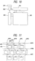
- Fig. 10 schematically shows a liquid crystal display panel using p-SiTFTs.
- a panel display circuit 305 including, as switching elements, p-SiTFTs arrayed in a matrix pattern is connected to a vertical shift register 303 and a horizontal shift register 304.
- TV video signals supplied from a video signal circuit 301 are written into pixels in the display circuit 305 through the vertical shift register 303 and the horizontal shift register 304.
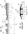
- Fig. 30 shows a section of a p-SiTFT.
- Source and drain regions each consisted of an n+-type diffusion layer 1403 and an n ⁇ -type diffusion layer 1407, for example, are formed in thin-film polysilicon on a quartz or glass substrate 1401.
- a channel between the source and drain regions is on-off controlled by applying a voltage to a gate electrode 1406 of polysilicon formed on both the regions with the intervention of a gate insulating film 1405.
- the n ⁇ -type diffusion layer 1407 is formed for the purpose of relieving the electric field just below the gate electrode, particularly, in the vicinity of the drain, and serves to effectively improve the source-drain leak current and withstand voltage of the TFT.
- Denoted by 1408 is a source/drain electrode made of, e.g., aluminum
- 1410 is an interlayer insulating film made of, e.g., a silicon oxide film
- 1409 is a surface protection film made of, e.g., a silicon nitride film.
- An equivalent circuit of the foregoing liquid crystal panel is shown in Fig. 11.
- Pixel electrodes 406 are arranged in one-to-one relation to intersections between a plurality of signal lines 401A to 401D and a plurality of scan lines 402A to 402D, and a TFT 403 is connected at its drain to each of the pixel electrodes 406.
- the signal lines 401A to 401D are connected to respective sources of the TFTs 403 for each column, and the scan lines 402A to 402D are connected to respective gates of the TFTs 403 for each row.
- Video signals supplied through the signal lines 401A to 401D are written into the pixel electrodes 106.
- the drain of each TFT 403 is also connected to one electrode of a hold capacity 404 for holding the written charge for a sufficiently long period of time.
- the other electrode terminal 405 of the hold capacity 404 is connected to a potential common to all the pixels or the pixels for each row.
- the TFT is required to operate at a high speed.
- Known techniques for providing a p-Si thin film which can satisfactorily be used realize such a high-speed operation are as follows: (1) so-called long time annealing process wherein silane gas is decomposed by heat under reduced pressure to deposit p-Si which is then annealed for a long time at about 600 °C to develop grain-like p-Si on the order of several microns for increased carrier mobility, and (2) so-called hydrogenating process wherein silane gas is decomposed by heat under reduced pressure to deposit p-Si on which a film containing a plenty of hydrogen (e.g., a nitride film formed by the plasma CVD process) is deposited, followed by heat treatment to couple the hydrogen in the film to traps in the polysilicon boundary for increased carrier mobility.
- a film containing a plenty of hydrogen e.g., a nitride film formed by the plasma CVD process
- the above conventional process have had the following technical problems to be solved. Specifically, since the long time annealing process of (1) requires a long time for processing, a throughput is reduced, which necessarily pushes up a cost in mass-production.
- the plasma nitride film 1409 used as the surface protection film, shown in Fig. 30, can be used as a supply source for hydrogen. After depositing the nitride film, heat treatment is performed in hydrogen gas for about 30 minutes at 450 °C, for example, for diffusion of hydrogen.
- the carrier mobility of p-SiTFTs obtained by such a step is not sufficiently high and the rising characteristic of a current in the sub-threshold region is not satisfactory.
- the display device of the present invention is arranged as follows.
- the active matrix substrate in a display device including a liquid crystal held between an active matrix substrate made up by arranging thin film transistors thereon, each using polycrystalline silicon as a semiconductor layer, in one-to-one relation to intersections between a plurality of signal lines and a plurality of scan lines, and an opposite substrate opposed to the active matrix substrate, the active matrix substrate includes a film having tensile stress disposed at least below or above the semiconductor layer.
- the present invention also involves a manufacture method for a display device.
- the active matrix substrate is made up by arranging a film having tensile stress at least below or above the semiconductor layer.
- the present invention involves various forms.
- the film having tensile stress may be disposed below a wiring layer for making up the signal line or the scan line which is in the lowermost position with respect to a layer of the liquid crystal layer as a reference.
- the polycrystalline silicon semiconductor layer may be sandwiched between a first film, having tensile stress, for suppressing diffusion of hydrogen and a second thin film for supplying hydrogen to the polycrystalline silicon. That is to say, the first film and the second film may be positioned one above the other with the intervention of the polycrystalline silicon therebetween.
- the active matrix substrate includes a first thin film for suppressing diffusion of hydrogen and a second thin film for supplying hydrogen to polycrystalline silicon, these first and second films being positioned one above the other with the intervention of polycrystalline silicon therebetween, hydrogen to be coupled to silicon atoms in the polycrystalline silicon is supplied from one film, and the hydrogen once coupled to the silicon atoms is suppressed from diffusing by the other film. Therefore, hydrogen can remain stably in the polycrystalline silicon. As a result, the mobility and rising characteristic of the polycrystalline silicon can be improved to hold down variations in device characteristics. Further, the display device of the present invention can display a liquid crystal image in very high fineness. Additionally, due to a small leak current between the source and the drain, the pixel electrode can hold charges for a longer time, which results in a display image having a good contrast ratio.
- the display device includes a liquid crystal held between a semiconductor substrate, which has pixel electrodes arranged in one-to-one relation to intersections between a plurality of signal lines and a plurality of scan lines, has driving circuits provided in peripheral portions of the pixel electrodes for driving the respective pixel electrode, and is partly removed in portions below pixel display areas where the pixel electrodes are provided, allowing light to transmit through the semiconductor substrate to enter the pixel display areas, and an opposite substrate opposed to the active matrix substrate, wherein a field oxide film is provided below each of the pixel display areas of the semiconductor substrate so as to extend toward the peripheral portion where the driving circuit is provided, the removed part of the semiconductor substrate is positioned inwardly of a position at which the field oxide film terminates, and the film having tensile stress is disposed in the peripheral portion where the driving circuit is provided.
- the mechanical strength is improved and a high-quality image can be displayed
- Figs. 1A and 1B are schematic views showing one example of a semiconductor substrate in successive steps which can be applied to the display device of the present invention.
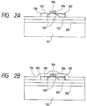
- Figs. 2A and 2B are schematic views showing the one example of a semiconductor substrate in subsequent successive steps which can be applied to the display device of the present invention.
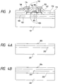
- Fig. 3 is a schematic view showing the one example of a semiconductor substrate in a subsequent step which can be applied to the display device of the present invention.
- Figs. 4A and 4B are schematic views showing an other example of a semiconductor substrate in successive steps which can be applied to the display device of the present invention.
- Figs. 5A and 5B are schematic views showing the other example of a semiconductor substrate in subsequent successive steps which can be applied to the display device of the present invention.
- Fig. 6 is a schematic view showing the other example of a semiconductor substrate in a subsequent step which can be applied to the display device of the present invention.
- Fig. 7 is a schematic view showing the other example of a semiconductor substrate in a subsequent step which can be applied to the display device of the present invention.
- Fig. 8 is a schematic view showing one example of a TFT which can be applied to the display device of the present invention.
- Fig. 9 is a schematic view showing another example of a TFT which can be applied to the display device of the present invention.
- Fig. 10 is a schematic view showing one example of the display device of the present invention.
- Fig. 11 is a diagram showing one example of an equivalent circuit of the display device of the present invention.
- Fig. 12 is a schematic view showing one example of a pixel portion in the display device of the present invention.
- Fig. 13 is a schematic view showing one example of the display device of the present invention.
- Fig. 14 is a schematic view showing one example of an active matrix substrate which can be applied to the display device of the present invention.
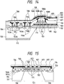
- Fig. 15 is a schematic view showing another example of the display device of the present invention.
- Fig. 16 is a schematic view showing another example of an active matrix substrate which can be applied to the display device of the present invention.
- Fig. 17 is a schematic view showing still another example of the display device of the present invention.
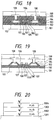
- Fig. 18 is a schematic view showing another example of a TFT which can be applied to the display device of the present invention.
- Fig. 19 is a schematic view showing still another example of a TFT which can be applied to the display device of the present invention.
- Fig. 20 is a schematic view for explaining a film structure of an active matrix substrate which can be applied to the display device of the present invention.
- Fig. 21 is a schematic view showing still another example of a semiconductor substrate which can be applied to the display device of the present invention.
- Fig. 22 is a schematic view showing still another example of the display device of the present invention.
- Fig. 23 is a diagram showing one example of an equivalent circuit of the display device of the present invention.
- Fig. 24 is a schematic view showing one example of a pixel portion in the display device of the present invention.
- Fig. 25 is a schematic view showing still another example of a semiconductor substrate which can be applied to the display device of the present invention.
- Fig. 26 is a schematic view showing still another example of a semiconductor substrate which can be applied to the display device of the present invention.
- Fig. 27 is a plan view of Fig. 26.
- Fig. 28 is a schematic view showing still another example of a semiconductor substrate which can be applied to the display device of the present invention.
- Fig. 29 is a schematic view showing still another example of a semiconductor substrate which can be applied to the display device of the present invention.
- Fig. 30 is a schematic view showing one example of a structure of a prior art TFT.
- the display device of the present invention can be applied to various liquid crystal display devices such as of transmission, reflection, projection and spectacle types.
- an active matrix substrate includes a first thin film for suppressing diffusion of hydrogen and a second thin film for supplying hydrogen to polycrystalline silicon, these first and second films being able to position one above the other with the intervention of polycrystalline silicon therebetween.
- the first and second films may be each formed of silicon nitride.
- a silicon nitride film formed by the plasma CVD process as the film for supplying hydrogen
- a silicon nitride film formed by the reduced-pressure CVD process as the film for suppressing diffusion of hydrogen, for example, a very effective improvement can be achieved while using conventional semiconductor materials.
- the first film may be formed of a film developing tensile stress for silicon
- the second film may be formed of a film developing compressive stress for silicon.
- a transmission type liquid crystal display panel using a membrane structure for example, by using a silicon nitride film formed by the reduced-pressure CVD process so that the compressive stress attributable to a silicon nitride film formed by the plasma CVD process or any other film (such as a silicon oxide film) is cancelled out, wrinkles and slacks of the membrane can be suppressed and, hence, superior characteristics of a TFT can be maintained.
- the active matrix substrate may be formed of a glass or quartz substrate.
- the active matrix substrate may be formed of a single crystal silicon substrate. In the latter case, by integrating both switching devices formed of single crystal silicon and pixel switching TFTs formed of polycrystalline on the substrate, the TFTs having better characteristics than conventional can be installed in a liquid crystal display panel with high-speed driving circuits. As a result, the panel can display an image at a higher degree of fineness.
- part of a single crystal silicon substrate may be removed to provide a light transmissive substrate for application to a transmission type panel.
- the active matrix substrate may be one including a scanning circuit at least part of which is made up by switching devices formed of single crystal silicon.
- a scanning circuit at least part of which is made up by switching devices formed of single crystal silicon.
- n1d1 N1 ⁇ /2
- n2d2 N2 ⁇ /2 (where N1 and N2 are both natural numbers, not 0)
- a support base being of, e.g., a silicon substrate.
- the support base 101 serves as a base of a semiconductor substrate for holding a liquid crystal between itself and an opposite substrate.
- 102 is a silicon nitride film formed on the support base 101 by the reduced-pressure CVD process, the film 102 having tensile stress.
- a polysilicon layer 104 is deposited and then thermally oxidized to form a gate insulating film 105.
- polysilicon is deposited on the gate insulating film 105 to form a gate 106, and ions are implanted to the polysilicon layer 104 to form a source 108 and a drain 107.
- the source 108 and the drain 107 are formed by using masks positioned to provide such an offset that the source and the drain are spaced from the gate electrode.
- a low-concentration electric field relieving layer 109 is formed by implanting ions in a low concentration to the polysilicon layer 104 with self-alignment using the gate.
- a silicon nitride film 111 is deposited thereon by the plasma CVD process.
- contacts 112 and then metal wirings 113, 114 are formed so that transistor electrodes are wired for further electrical connection.
- the substrate of the structure shown in Fig. 3 is obtained.
- additional upper layers are formed depending on functions of the display device to be manufactured. More specifically, on the substrate shown in Fig.
- a pixel electrode connected to the drain of the transistor, a signal line connected to the source of the transistor, a scan line connected to the gate of the transistor, an orienting film, and so on are formed to provide a semiconductor substrate which holds a liquid crystal layer between itself and an opposite substrate.
- a film having tensile stress i.e., the silicon nitride film 111 formed by the plasma CVD process, is disposed below a wiring layer for making up the signal line or the scan line which is in the lowermost position with respect to the liquid crystal layer as a reference.
- Implantation of hydrogen atoms into polysilicon is effective to improve characteristics of a polysilicon transistor in points of reducing an off-current and increasing an on-current.
- hydrogen atoms are diffused by annealing from the silicon nitride film 111 formed by the plasma CVD process into the polysilicon layer 104 for improving characteristics of the transistor.
- the annealing is advantageously performed at 350 °C to 550 °C for a period of about 10 minutes to 5 hours, but it may be performed, for example, at 450 °C for a period of about 30 minutes.
- the annealing may be performed by utilizing the heat history applied in any other suitable step. Carrying out the annealing in a further prolonged time is effective for further improvement.
- the annealing step can be made at any time after the silicon nitride film 111 has been formed.
- the silicon nitride film 111 formed by the plasma CVD process is deposited on the PSG film 110 in this embodiment, it may be deposited anywhere so long as hydrogen can be diffused into the polysilicon layer 104.
- the PSG film 110 may be replaced by the silicon nitride film 111.
- the silicon nitride film 102 formed by the reduced-pressure CVD process lies under the polysilicon layer 104, it serves to prevent hydrogen from diffusing downward from the polysilicon layer 104, enabling hydrogen atoms to be efficiently implanted into the polysilicon layer 104.
- the semiconductor substrate thus produced is applied to a liquid crystal display device, the number of pixels can be increased to achieve a finer pixel array of the panel because of a reduction in the size of each transistor, and the contrast ratio and the number of gradation steps can be increased because of a reduction in the off-current.
- liquid crystal display panels of the simple matrix type include, for example, ones using a ferroelectric liquid crystal as the liquid crystal, and using MIM devices or PN junction devices as the pixel portions.
- a second embodiment will be described with reference to Figs. 4A to 7.
- the present invention is applied to a transmission type liquid crystal display device.
- a support base 201 is formed of, e.g., a silicon substrate.
- a silicon nitride film 203 is formed by the reduced-pressure CVD process and a PSG film 204 is then deposited on the silicon nitride film 203, resulting in a structure shown in Fig. 4B.
- a transistor is formed thereon by similar steps in the above Embodiment 1.
- 205 is a polysilicon layer
- 206 is a gate insulating film
- 207 is a gate electrode
- 208 is a source
- 209 is a drain
- 210 is a low-concentration electric field relieving layer
- 211 is a PSG film
- 212 is a contact
- 213, 214 are metal wirings.
- a metal film 216 is formed.
- the metal film 216 is only required to be able to conduct electricity and shield light, and it can be formed of such a material as Ti, TiN or Al, for example.
- a silicon nitride film 217 is formed by the plasma CVD process.
- the substrate is then subjected to annealing so that hydrogen atoms are diffused from the silicon nitride film 217 formed by the plasma CVD process into the polysilicon layer 205 to improve characteristics of the transistor.
- a pixel electrode 219 for applying a voltage to the liquid crystal is formed to be connected with the wiring 214.
- the pixel electrode 219 is a transparent electrode and is formed of ITO.
- the metal film 216 is fixedly held at the peripheral potential of a display area and serves to establish a capacity between itself and the pixel electrode 219 for stabilizing a pixel electrode potential.
- the nitride film 217 is interposed between the pixel electrode 219 and the metal film 216, this embodiment has a merit of providing the larger capacity therebetween than the case of using an oxide film.
- the nitride film 217 may be replaced by any other suitable insulating film layer.
- a polyimide film is formed thereon, followed by rubbing to obtain a semiconductor substrate as one of paired substrates of a liquid crystal display device. A liquid crystal is sandwiched between the thus-obtained semiconductor substrate and an opposite substrate, thereby completing the liquid crystal display device.
- the opposite substrate comprises a support base, transparent electrodes, and a polyimide film subjected to rubbing.
- a liquid crystal display device adapted for color display can be obtained.
- the rear surface of the substrate 201 is partly etched so that the pixel display area is made transparent (as indicated by 220) to provide a transmission type display device.
- the oxide film 202 serves as an etching stop.
- One of materials causing tensile stress therein is a silicon nitride film formed by the reduced-pressure CVD process.
- a silicon nitride film formed by the reduced-pressure CVD process exists between the polysilicon layer 205 and the silicon nitride film 217 formed by the plasma CVD process, it would prevent diffusion of hydrogen atoms into the polysilicon layer 205 during the annealing, resulting in a disadvantage of no improvement in characteristics of the transistor. Therefore, the foregoing structure of the substrate according to this embodiment is advantageous for effective diffusion of hydrogen atoms.
- Fine adjustment of stresses in the films as required when partly thinning the substrate may be performed by setting initial design values such that the films slack slightly, and then etching the oxide film 202 by fluoric acid or the like.
- the driving circuits and the display areas can be both formed in an on-chip arrangement.
- the driving circuits can be of a single MOS structure or a CMOS structure.
- the driving circuits may be formed of polysilicon. It is possible to reduce the number of masks and simplify the manufacture steps by simultaneously carrying out some of the processes necessary to form the driving circuits and some of the processes necessary to form the display areas which can be made in common.
- the transistor size can be reduced and, hence, the number of pixels can be increased to achieve a finer pixel array of the panel. Furthermore, because of a reduction in the off-current, the contrast ratio and the number of gradation steps can be increased.
- a silicon substrate is used as the support base in this embodiment
- a transparent substrate such as a glass substrate may be used as the support base so that a liquid crystal display device may be manufactured without thinning the substrate in the display areas.
- a liquid crystal display device capable of displaying an image with a higher degree of fineness, the increased number of gradation steps, and a higher contrast ratio can also be provided because of improved transistor characteristics.
- the present invention is also applicable to a reflection type liquid crystal display device.
- the reflection type is advantageous in obtaining a higher opening rate.
- the silicon nitride film formed by the reduced-pressure CVD process provides a film having tensile stress in this embodiment.
- any other kind of film having tensile stress such as a SiON film containing oxygen atoms or a laminated film of a SiON film and a silicon nitride film, can also be applied to the display device of the present invention.
- the liquid crystal display device can be manufactured by the use of a semiconductor substrate including transistors of which on/off characteristics are efficiently improved by annealing.
- this embodiment is applied to a transmission type display device using a support base which is made transparent by etching, it is possible to provide the display device in which films in etched portions are under proper tension and switching transistors have improved on/off characteristics.
- the liquid crystal display device capable of displaying an image with a higher degree of fineness, the increased number of gradation steps, and a higher contrast ratio can also be provided.
- Fig. 8 is a schematic sectional view of an n+p-SiTFT which can be employed in the display device of the present invention.
- a silicon nitride film 102 is coated on a semiconductor or quartz substrate 101, and a channel, a source and a drain of the TFT are formed on the silicon nitride film 102.
- Denoted by reference numeral 103 is a high-concentration source/drain and 107 is a low-concentration source/drain for relieving an electric field.
- 105 is a gate insulating film formed of, e.g., a silicon nitride film, and 106 is polycrystalline silicon doped into n-type, for example.
- the so-called dual gate TFT having two gate electrodes at the same potential arranged in series between the source and the drain is thereby made up.
- 106' is an interlayer insulating film formed of, e.g., PSG (Phospho-Silicate Glass), and 108 is a source/drain electrode formed of, e.g., aluminum.
- 109 is a hydrogen supply source for hydrogenation which is formed of, e.g., a silicon nitride film.
- the silicon nitride film 109 doubles as a surface protection film for preventing intrusion of moisture and impurities from the outside to thereby ensure reliability of the TFT.
- the silicon nitride film 102 is formed by the thermal CVD process in which silane gas is thermally decomposed under reduced pressure at a temperature of 600 to 900 °C.
- the silicon nitride film 109 as a hydrogen supply source is formed by exciting a gas mixture of silane gas and ammonia gas or silane gas and N2O (laughing gas) under reduced pressure at a temperature of 200 to 400 °C for decomposition and deposition thereof in plasma. It is important for the interlayer insulating film 106' to allow high-speed diffusion of hydrogen. Hydrogenation of polycrystalline silicon is progressed to some extent during deposition of the silicon nitride film 109.
- the heat treatment in hydrogen gas or a gas mixture of hydrogen gas and inert gas such as nitrogen gas at a temperature of 350 to 500 °C for 10 to 120 minutes after the deposition.
- An upper limit of the treatment temperature is determined depending on the melting point of the aluminum electrodes or the temperature causing a separating action of hydrogen.
- the heat treatment at a temperature not lower than 500 °C is not desired.
- the hydrogenating effect is also rather abated at a temperature not lower than 500 °C. This is because the hydrogen once taken into the grain boundary of polycrystalline silicon separates again therefrom at such a temperature.
- the TFT shown in Fig. 8 is manufactured as follows. First, silane gas and ammonia gas are reacted with each other under reduced pressure of 1 mm to 760 mm Torr to deposit the silicon nitride film 102 with a thickness of 100 to 400 nm on an oxidized surface of the silicon (or quartz) substrate 101. Next, silane gas diluted by nitrogen is thermally decomposed under pressure of 0.1 to 1.0 Torr at 600 to 700 °C to deposit a polycrystalline silicon film with a thickness of 50 to 400 nm, which is then patterned to form regions for the source/drain 103.
- This process is effective not only to reduce parasitic resistance of the source/drain regions, but also to prevent a second-layer polycrystalline silicon 104 from being lost by overetching when source/drain contact holes are etched.
- An additional silicon nitride film of about 10 to 200 nm may be formed on the silicon nitride film 102 so that the underlying silicon nitride 102 will not be etched during patterning of the first-layer polycrystalline silicon.
- the second-layer polycrystalline silicon 104 is deposited in a thickness of 50 to 200 nm by the reduced-pressure CVD process.
- the thickness of the polycrystalline silicon is as thin as possible, because a leak current of the TFT is reduced correspondingly.
- the thickness of the deposited polycrystalline silicon film was set to 80 nm, taking into account a subsequent step of forming a thermal oxide film with a thickness of 80 nm at 1150 °C and variations process by process.
- the gate oxide film may also be of an ONO (Oxidized-Nitrided Oxide) film obtained by forming an oxide film and then nitriding and oxidizing it successively. After forming the gate oxide film, polycrystalline silicon becoming the gate electrode is deposited in a thickness of 100 to 500 nm, followed by high-concentration doping and patterning to form the gate electrode 106.
- ONO Oxidized-Nitrided Oxide
- the interlayer insulating layer 106 of a PSG film is deposited in a thickness of 100 to 500 nm by the CVD process.
- the interlayer insulating layer 106 may be formed of, e.g., NSG (Non-Doped Silicate Glass) or BPSG (Boron-Phospho Silicate Glass).
- electrode materials are general materials used in common semiconductor and TFT processes, for example, another kind of Al alloy, W, Ta, Ti, Cu, Cr, Mo, or silicide thereof.
- the deposited electrode material is patterned to form the source/drain electrodes 108.
- a gas mixture of silane gas and N2O gas is decomposed in plasma at 200 to 400 °C to deposit the silicon nitride film 109 of 600 nm.
- heat treatment is performed in hydrogen gas at 450 °C for 30 minutes.
- the TFT thus formed is applied to a liquid crystal display panel.
- FIG. 10 schematically shows the liquid crystal display panel of this embodiment.
- a panel display circuit 305 including, as switching elements, p-SiTFTs arrayed in a matrix pattern is connected to a vertical shift register 303 and a horizontal shift register 304.
- TV video signals supplied from a video signal circuit 301 are written into pixels in the display circuit 305 through the vertical shift register 303 and the horizontal shift register 304.
- Denoted by 302 is a synch circuit for establishing the timed relationship between the two shift registers 303 and 304.
- FIG. 11 An equivalent circuit of the liquid crystal panel is shown in Fig. 11.
- Pixel electrodes 406 are arranged in one-to-one relation to intersections between a plurality of signal lines 401A to 401D and a plurality of scan lines 402A to 402D, and a TFT 403 is connected at its drain to each of the pixel electrodes 406.
- the signal lines 401A to 401D are connected to respective sources of the TFTs 403 for each column, and the scan lines 402A to 402D are connected to respective gates of the TFTs 403 for each row.
- Video signals supplied through the signal lines 401A to 401D are written into the pixel electrodes 106.
- each TFT 403 is also connected to one electrode of a hold capacity 404 for holding the written charge for a sufficiently long period of time.
- the other electrode terminal 405 of the hold capacity 404 is connected to a potential common to all the pixels or the pixels for each row.
- Fig. 12 schematically shows a plan structure of the pixel portion.
- One pixel is surrounded by two signal lines 501A, 501B adjacent to each other and two scan lines 502A, 502B adjacent to each other.
- the source of the TFT formed of a polycrystalline silicon film 503 is connected to the signal line 501A through a contact hole 504 for writing signal charges into the drain of the TFT through the two gates.
- 505 is a contact for interconnecting the TFT and a metal electrode 506, and the metal electrode 506 is connected to a transparent pixel electrode 508 via a through-hole 507.
- 509 is an opening in a light shielding film which prevents unwanted light from entering the TFT.
- Fig. 13 is a sectional view taken along line 13 - 13 in Fig. 12.
- a silicon nitride film 102 is coated on the silicon or quartz substrate 101.
- a silicon oxide film 202 of 10 to 100 nm is formed on the silicon nitride film 102 to separate the TFT from the silicon nitride film 102.
- the TFT has low-concentration n-type layers 107 for relieving an electric field and a high-concentration source/drain 103 which are in opposite relation to two polysilicon gate electrodes 106 with the intervention of a gate oxide film 105 therebetween.
- the source and drain electrodes 108 each comprise a laminated film of an Al film 108A and a Ti film 108B for easier ohmic connection to a pixel electrode 603.
- a light shielding film 602 is formed of, e.g., a TiN film and is separated from the source and drain electrodes with the intervention of, e.g., a PSG film 601 therebetween and from the TFT with the intervention of, e.g., a BPSG film 106'' therebetween.
- a plasma nitride film 109 for hydrogenation is disposed between the light shielding film 602 and the pixel electrode 603.
- the hydrogenating effect can also sufficiently be achieved with the plasma nitride film disposed above the light shielding film.
- the PSG film 601 may be replaced by a nitride film for hydrogenation.
- 610 is an orienting film formed of, e.g., a PIQ film for orienting a liquid crystal.
- An active matrix substrate is made up by the above-mentioned components starting from the substrate 101 and ending at the orienting film 610 shown in Fig. 13.
- a TN liquid crystal 611 is held between the active matrix substrate and an opposite substrate 621 on an undersurface of which an orienting film 626, a protection film 625 and a transparent electrode 624 are provided as shown. Further, a color filter 623 formed of pigments, for example, is disposed corresponding to an opening in the light shielding film 602, and a black matrix 622 formed of Cr, for example, is disposed corresponding to the remaining portion of the light shielding film 602.
- the panel With the liquid crystal display panel thus manufactured, the panel was able to display a finer liquid crystal image with pixel size not larger than 20 ⁇ m square. Also, a reduction in the source - drain leak current realized the panel having a prolonged charge hold time of the pixel electrode and a good contrast ratio. Furthermore, the number of defects such as white or black dots was small and the production yield was increased remarkably.
- Fig. 9 is a schematic sectional view of the so-called bottom gate TFT having channel polysilicon positioned above a gate electrode, which TFT can be applied to the display device of the present invention.
- a silicon nitride film 102 is coated on a semiconductor, quartz or glass substrate 101, and a silicon oxide film 202 as an etching stop is formed on the silicon nitride film 102.
- the TFT may have a structure having no silicon oxide film 202.
- 106 is a gate electrode of the TFT formed of, e.g., n+-type polycrystalline silicon.
- a metal as Al, Cr, Ta, TaN or Ti can also be used as the gate electrode.
- 105 is a gate insulating film formed of, e.g., a silicon oxide film, and 201 is a channel portion formed of polycrystalline silicon.
- the channel portion 201 may be formed of an Al2O3 film, a SiN film, or a laminated film thereof.
- 107 is an n-type electric field relieving region of low concentration and 103 is a source/drain region of high concentration.
- the TFT may be of p-type.
- 106'' is an interlayer insulating film formed of, e.g., BPSG and 108 is a metal electrode for the source/drain.
- 104 is polysilicon and 109 is a silicon nitride film.
- the two silicon nitride films 109 and 102 serve respectively to supply hydrogen and prevent diffusion of hydrogen.
- the film for effectively preventing diffusion of hydrogen is advantageously a silicon nitride film formed by the reduced-pressure CVD process or the thermal CVD process.
- the silicon nitride film formed by the plasma CVD process which is effective as a supply source for hydrogen, can double as a surface protection film. Also, since the channel portion is close to the silicon nitride film formed by the plasma CVD process, the hydrogenating effect can be enhanced and matching between the manufacture processes can be improved.
- Fig. 18 is a schematic view of a TFT which can be applied to the display device of the present invention.
- a hydrogen supply source for hydrogenation is disposed below a metal electrode.
- This TFT has the same sectional structure as in the above Embodiment 3. Accordingly, a substrate 101, a silicon nitride film 102, a high-concentration source/drain region 103, an electric field relieving region 107, a gate electrode 106, a gate insulating film 105, a source/drain metal electrode 108, etc. can be formed by using the materials and the processes described above in connection with the Embodiment 3.
- This embodiment is different from the Embodiment 3 in that an interlayer insulating film 1106 between the gate electrode and the Al metal electrode is used as a supply source for hydrogen.
- the interlayer insulating film 1106 was formed of a silicon nitride film formed by the plasma CVD process and having a thickness of 800 nm in this embodiment. This thickness was determined in consideration of the parasitic capacity between wirings and a probable incidence of short-circuit failures, and can be changed with a certain degree of freedom.
- the film having a thickness not less than 10 nm can sufficiently function as the supply source for hydrogen.
- an etching stop layer e.g., a silicon oxide film, having a thickness not less than 50 nm may be formed on the silicon nitride film (PCVD).
- 109 is a surface protection film formed of PSG, BPSG, SiON or NSG, as well as a silicon nitride film formed by the plasma CVD process.
- Fig. 19 is a schematic view of a TFT which can be applied to the display device of the present invention.
- a supply source for hydrogen or a film for preventing diffusion of hydrogen is used as a gate insulating film.
- This TFT has the same sectional structure as in the above Embodiment 3. Accordingly, a substrate 101, a silicon nitride film 102, a high-concentration source/drain region 103, an electric field relieving region 107, a gate electrode 106, a interlayer insulating film 106', a source/drain metal electrode 108, etc. can be formed by using the materials and the processes described above in connection with the Embodiment 3.
- a gate insulating film 1105 may be formed of an ONO film.
- 102 was formed of a silicon nitride film by the thermal CVD process, and the gate insulating film was formed of a silicon nitride film by the plasma CVD process.
- a thickness of the gate insulating film is preferably in the range of 10 nm to 200 nm.
- 150 nm was selected for matching with threshold values of the TFT.
- the gate insulating film may be of a laminated film of a silicon nitride film and a silicon oxide film.
- a thin silicon oxide film is preferably provided as an etching stop during the patterning just below the gate electrode.
- the structure of this embodiment is applicable to a P-channel TFT, an N-channel TFT, and a bottom gate TFT like the Embodiment 2.
- Fig. 14 is a sectional view of an active matrix substrate (TFT substrate) of a transmission type liquid crystal display device in which the TFT shown in the Embodiment 3 is used as a pixel driving switch, and a signal line driving circuit and a scan line driving circuit, including a shift register, are integrated in bulk silicon.
- the circuit in the bulk silicon is of a CMOS structure, but not limited to the illustrated structure.
- 701 is a silicon substrate
- 702 is a thick oxide film for device separation
- 703A is a low-concentration source/drain of an NMOS transistor
- 703B is a high-concentration source/drain of the NMOS transistor.
- 704 is a p-type well of the NMOS transistor, 705 is a gate oxide film, 706 is a polysilicon gate electrode, and 708 is a source/drain electrode.
- 710A is a low-concentration source/drain of a PMOS transistor, 710B is a high-concentration source/drain, and 712 is an oxide film on the rear surface of the substrate.
- the TFT portion has the same structure as shown in Fig. 13 and will not be hence described here.
- the substrate silicon is removed in the TFT portion.
- 711 is an etching end which defines the size of a display area.
- the oxide film 712 serves as an etching mask used when removing the substrate silicon.
- the portion below the thick oxide film 702 is etched away.
- Fig. 15 shows a section of the liquid crystal display device in which the TFT substrate of Fig. 14 is mounted.
- 720 is a support comprising substrate silicon
- 721 is a transparent area where the substrate silicon is etched away and which becomes a display area of the panel.
- 722 is TFT
- 725 is a portion connecting a pixel electrode 603 with the TFT.
- Identical components to those in Fig. 14 are denoted by the same reference numerals and will not be described here.
- the TFT substrate shown in Fig. 14 is disposed parallel to an opposite substrate 621 with a liquid crystal material 611 sealed between the two substrates.
- a spacer 724 is provided so that the liquid crystal material 611 is maintained at a thickness designed in consideration of optical characteristics of the liquid crystal.
- a transparent common electrode 625 common to all the pixels or the pixels for each row is disposed in a position opposite to pixel electrodes 603 for applying a voltage to the liquid crystal. Since this embodiment is adapted for a full-color display panel, color filters 623 formed of dyes or pigments are arranged on the opposite substrate 621, whereas the remaining portions between the pixels and above peripheral driving circuits are shielded against light by a black matrix 622.
- the liquid crystal material 611 is preferably of a TN (Twist-Nematic) liquid crystal, but may be of an STN (Super Twist-Nematic) liquid crystal, an FLC (Ferroelectric Liquid Crystal), or a PDLC (Polymer-Diffused Liquid Crystal) from the structural viewpoint.
- a TN or STN liquid crystal or an FLC polarizing plates are required to be disposed above and below the display device in the crossed Nichol state.
- a backlight necessary for display may be irradiated from above or below as viewed in Fig. 15. To sufficiently shield light, the backlight is advantageously irradiated from above in the structure of this embodiment.
- Film arrangements in the display area shown in Fig. 14 include inventive measures below for the purpose of improving panel characteristics of this embodiment.
- a liquid crystal display device having the larger number of gradation steps and a higher contrast ratio than conventional was obtained.
- a single crystal silicon substrate of high quality being used to form driving circuits, not only a reduction in size of the display device, but also an improvement in yield were achieved.
- a display device having an increased yield of the membrane manufacture steps, high reliability, high transmissivity by virtue of reduced reflection of light, and high display quality was provided.
- This embodiment is to construct a reflection type liquid crystal display device using an active matrix substrate shown in Fig. 16.
- the active matrix substrate shown in Fig. 16 is similarly structured to the substrate shown in Fig. 14 except that the former substrate has no portion hollowed or partly removed by etching, and includes an opaque metal electrode 908 for reflecting incident light.
- 909 is a silicon nitride film which is formed by the plasma CVD process and doubles as a passivation film here.
- a reflection type liquid crystal display device as shown in Fig. 17 was manufactured by using the active matrix substrate thus structured. Unlike the transmission type liquid crystal display device shown in Fig. 15, the liquid crystal display device shown in Fig.
- Fig. 17 has no hollowed portion through which incident light transmits, and reflects the incident light by the opaque metal electrode 908 for displaying an image.
- 911 is a liquid crystal
- 912 is a polarizer.
- a liquid crystal panel was manufactured by using a TN type as the liquid crystal, and the incident light was condensed by using a polarizing beam splitter to display an image. The resulting image was superior in having the increased number of gradation steps and a higher contrast ratio.
- a liquid crystal display device was manufactured by omitting the polarizer 912 from the liquid crystal display device shown in Fig. 17. Then, in this embodiment, a liquid crystal panel was manufactured by using a PDLC (Polymer-Diffused Liquid Crystal) as the liquid crystal, and an image was displayed by using a Schlieren optical system. The resulting image was superior in having the increased number of gradation steps and a higher contrast ratio.
- PDLC Polymer-Diffused Liquid Crystal
- a projection type liquid crystal display device was manufactured by combining each of the liquid crystal display devices shown in Figs. 15 and 17 with a magnifying optical system. A superior image was also obtained in this embodiment.
- a so-called spectacle type liquid crystal display device was manufactured by assembling each of the liquid crystal display devices shown in Figs. 15 and 17 in spectacles.
- the manufactured display device was able to display the same image in both right and left panels, or a stereoscopic image by the right and left panels. An image obtained in this embodiment was good.
- FIG. 10 A schematic view of a liquid crystal display panel of this embodiment is shown in Fig. 10.
- a panel display circuit 305 including, as switching elements, p-SiTFTs arrayed in a matrix pattern is connected to a vertical shift register 303 and a horizontal shift register 304.
- TV video signals supplied from a video signal circuit 301 are written into pixels in the display circuit 305 through the vertical shift register 303 and the horizontal shift register 304.
- Denoted by 302 is a synch circuit for establishing the timed relationship between the two shift registers 303 and 304.
- FIG. 23 An equivalent circuit of the liquid crystal panel is shown in Fig. 23.
- Pixel electrodes 406 are arranged in one-to-one relation to intersections between a plurality of signal lines 401A to 401D and a plurality of scan lines 402A to 402D, and a TFT 403 is connected at its drain to each of the pixel electrodes 406.
- the signal lines 401A to 401D are connected to respective sources of the TFTs 403 for each column, and the scan lines 402A to 402D are connected to respective gates of the TFTs 403 for each row.
- Video signals supplied through the signal lines 401A to 401D are written into the pixel electrodes 106.
- each TFT 403 is also connected to one electrode of a hold capacity 404 for holding the written charge for a sufficiently long period of time.
- the other electrode terminal 405 of the hold capacity 404 is connected to a potential common to all the pixels or the pixels for each row. While this embodiment is described in connection with the liquid crystal display device of the so-called active matrix type using TFTs, the present invention is not limited to this type of display device, but also applicable to liquid crystal display panels of the simple matrix type using, for example, MIM devices or PN junction devices arranged in one-to-one relation to the intersections between the signal lines and the scan lines.
- Fig. 24 schematically shows a plan structure of a pixel portion.
- One pixel is surrounded by two signal lines 501A, 501B adjacent to each other and two scan lines 502A, 502B adjacent to each other.
- the source of the TFT formed of a polycrystalline silicon film 503 is connected to the signal line 501A through a contact hole 504 for writing signal charges into the drain of the TFT through two gates.
- 505 is a contact for interconnecting the TFT and a metal electrode 506, and the metal electrode 506 is connected to a transparent pixel electrode 508 via a through-hole 507.
- 509 is an opening in a light shielding film which prevents unwanted light from entering the TFT.
- Fig. 25 is a sectional view taken along line 25 - 25 in Fig. 24.
- a silicon nitride film 102 is coated on the silicon or quartz substrate 101.
- a silicon oxide film 202 of 10 to 100 nm is formed on the silicon nitride film 102 to separate the TFT from the silicon nitride film 102.
- the TFT has low-concentration n-type layers 107 for relieving an electric field and a high-concentration source/drain 103 which are in opposite relation to two polysilicon gate electrodes 106 with the intervention of a gate oxide film 105 therebetween.
- the source and drain electrodes 108 each comprise a laminated film of an Al film 108A and a Ti film 108B for easier ohmic connection to a pixel electrode 603.
- a light shielding film 602 is formed of, e.g., a TiN film and is separated from the source and drain electrodes with the intervention of, e.g., a PSG film 601 therebetween and from the TFT with the intervention of, e.g., a BPSG film 106'' therebetween.
- 610 is an orienting film formed of, e.g., a PIQ film for orienting a liquid crystal.
- An active matrix substrate is made up by the above-mentioned components starting from the substrate 101 and ending at the orienting film 610 shown in Fig. 25.
- a TN liquid crystal 611 is held between the active matrix substrate and an opposite substrate 621 on an undersurface of which an orienting film 626, a protection film 625 and a transparent electrode 624 are provided as shown.
- a color filter 623 formed of pigments for example, is disposed corresponding to an opening in the light shielding film 602
- a black matrix 622 formed of Cr for example, is disposed corresponding to the remaining portion of the light shielding film 602.
- Fig. 22 shows a section of the liquid crystal display panel of this embodiment, including a pixel display area and a peripheral driving circuit portion.
- 701 is a silicon substrate
- 702 is a thick oxide film (field oxide film) for device separation
- 703A is a low-concentration source/drain of an NMOS transistor
- 703B is a high-concentration source/drain of the NMOS transistor.
- 704 is a p-type well of the NMOS transistor and 706 is a polysilicon gate electrode.
- 720 is a support comprising substrate silicon
- 721 is a transparent area where the substrate silicon is etched away and which becomes a display portion (pixel display area) of the panel.
- the TFT substrate (semiconductor substrate) shown in Fig. 22 is disposed parallel to an opposite substrate 621 with a liquid crystal material 611 sealed between the two substrates.
- a spacer 724 is provided so that the liquid crystal material 611 is maintained at a thickness designed in consideration of optical characteristics of the liquid crystal.
- a transparent common electrode 625 common to all the pixels or the pixels for each row is disposed in a position opposite to pixel electrodes 603 for applying a voltage to the liquid crystal. Since this embodiment is adapted for a full-color display panel, color filters 623 formed of dyes or pigments are arranged on the opposite substrate 621, whereas the remaining portions between the pixels and above peripheral driving circuit portions are shielded against light by a black matrix 622.
- the liquid crystal material 611 is preferably of a TN (Twist-Nematic) liquid crystal, but may be of an STN (Super Twist-Nematic) liquid crystal, an FLC (Ferroelectric Liquid Crystal), or a PDLC (Polymer-Diffused Liquid Crystal) from the structural viewpoint.
- a TN or STN liquid crystal or an FLC polarizing plates are required to be disposed above and below the display device in the crossed Nichol state. A backlight necessary for display may be irradiated from above or below as viewed in Fig. 22.
- Fig. 21 schematically shows the vicinity of a portion of the TFT substrate (semiconductor substrate) shown in Fig. 22 where the silicon is removed.
- 1 is a Si substrate
- 2 is a SiN film formed by the reduced-pressure CVD process
- 3 is a field oxide film
- 4 is an end position of the portion of the TFT substrate (semiconductor substrate) where the Si substrate 1 has been partly etched away to form a transparent pixel display area.
- 5 denotes a portion at which the field oxide film 3 terminates in a bird's beak shape, as shown in Fig. 21, when it is formed by the LOCOS process.
- the field oxide film 3 is a film having compressive stress and hence would cause a slack if it is not laminated with another film having tensile stress.
- a film having tensile stress i.e., the SiN film 2 formed by the reduced-pressure CVD process is disposed adjacent to the field oxide film 3, as shown in Fig. 21, for relieving the moment applied to the field oxide film 3.
- the field oxide film 3 having compressive stress must be terminated anywhere. Accordingly, as shown in Fig.
- the end 6 of the SiN film 2 formed by the reduced-pressure CVD process is positioned outwardly of the end position 4 of the portion where the Si substrate 1 has been partly etched away.
- a peripheral driving circuit is provided below the end 6 of the SiN film 2. If the end 6 of the SiN film 2 is positioned inwardly of the end position 4 of the removed portion of the Si substrate 1 conversely to the above, tensile stress of the SiN film 2 would act through the field oxide film 3 having compressive stress and, hence, the film laminated on the field oxide film 3 would become hard to properly tense.
- the end 6 of the SiN film 2 is positioned outwardly of the terminated position 5 of the field oxide film 3 so that the end 6 of the SiN film 2 is positioned as close as possible to the Si substrate 1.
- the laminated films were held under proper tension and showed the good mechanical strength.
- the panel was able to display a high-quality image stably for a long period of time.
- Fig. 26 schematically shows part of a semiconductor substrate.
- 1 is a Si substrate
- 2 is a SiN film formed by the reduced-pressure CVD process
- 3 is a field oxide film
- 4 is an end position of the portion of the TFT substrate (semiconductor substrate) where the Si substrate 1 has been partly etched away to form a transparent pixel display area.
- 5 denotes a portion at which the field oxide film 3 terminates.
- 6 denotes an end of the SiN film 2 formed by the reduced-pressure CVD process
- 7 denotes a thin oxide film.
- 3' is a field oxide film and 8 is an edge of the field oxide film 3'.
- Fig. 27 is a plan view of Fig. 26 as viewed from above.
- the same reference numerals denote identical components to those in Fig. 26.
- a film having tensile stress i.e., the SiN film 2 formed by the reduced-pressure CVD process is disposed such that its end 6 extends over the field oxide film 3' beyond the thin oxide film 7.
- This structure enabled the two films 2 and 3 (3') to be positioned adjacent to the Si substrate 1 without causing edge damages.
- the field oxide films 3, 3' and the SiN film 2 were held under proper tension and good stability.
- a liquid crystal display panel was manufactured by using the thus-constructed semiconductor substrate in a like manner to the above Embodiment 12. The resulting display panel was superior and able to display a high-quality image stably for a long period of time.
- Fig. 28 schematically shows arrangements of a thin film transistor (TFT), a pixel electrode, wirings and so on which are formed the semiconductor substrate shown in Fig. 26.
- TFT thin film transistor
- 901 is a channel portion of the TFT
- 902 is an interlayer insulating layer
- 903 is a pixel electrode (ITO).
- 904 is a low-concentration source/drain layer close to a gate
- 906 is a gate
- 907 is a source/drain.
- 908A is an AlSi wiring layer
- 908B is a Ti or TiN layer
- 909, 910 are interlayer insulating layers.
- the SiN film 2 having tensile stress is disposed on the TFT.
- the SiN film 2 is formed over a wider area, it is easy to fix the SiN film 2 in the peripheral driving circuit area.
- a liquid crystal display panel was manufactured by using the thus-constructed semiconductor substrate in a like manner to the above Embodiment 12. The resulting display panel was superior and able to display a high-quality image stably for a long period of time.
- the technique described in this embodiment can be applied to not only liquid crystal display devices, but also other devices which are manufactured by partly removing Si substrates, such as pressure sensors and acceleration sensors.
- Fig. 29 schematically shows part of a semiconductor substrate with a pixel electrode, wirings and so on omitted.
- components denoted by the same reference numerals as those in Fig. 26 or 28 are the same as those in Fig. 26 or 28.
- a SiN film 2 formed by the reduced-pressure CVD process is disposed under the TFT, but a SiN film 1002 formed by the reduced-pressure CVD process is left on a field oxide film 3. While an end 6 of the SiN film 2 appears as being terminated at the illustrated position in Fig. 29, the SiN film 2 is actually spread over other section areas like mesh for relieving stress to increase stability.
- a gate of a peripheral circuit is formed on the field oxide film 3 and the SiN film 2.
- This structure increases an effective threshold value of a field MOS so that a high-concentration impurity layer which is usually formed as a channel stop layer in a region 1003 may be dispensed with.
- this embodiment enabled the MOS structure having higher resistance to be produced by simplified manufacture steps.
- a liquid crystal display panel was manufactured by using the thus-constructed semiconductor substrate in a like manner to the above Embodiment 12. The resulting display panel was superior and able to display a high-quality image stably for a long period of time. Consequently, this embodiment can provide a display device which has the good mechanical strength and can stably display a high-quality image.
Landscapes
- Physics & Mathematics (AREA)
- Nonlinear Science (AREA)
- Mathematical Physics (AREA)
- Chemical & Material Sciences (AREA)
- Crystallography & Structural Chemistry (AREA)
- General Physics & Mathematics (AREA)
- Optics & Photonics (AREA)
- Liquid Crystal (AREA)
- Thin Film Transistor (AREA)
Applications Claiming Priority (9)
| Application Number | Priority Date | Filing Date | Title |
|---|---|---|---|
| JP137320/94 | 1994-06-20 | ||
| JP13732094 | 1994-06-20 | ||
| JP13732094A JP3109956B2 (ja) | 1994-06-20 | 1994-06-20 | 表示装置 |
| JP137319/94 | 1994-06-20 | ||
| JP13731994 | 1994-06-20 | ||
| JP13732194 | 1994-06-20 | ||
| JP137321/94 | 1994-06-20 | ||
| JP13732194 | 1994-06-20 | ||
| JP13731994A JP3155886B2 (ja) | 1994-06-20 | 1994-06-20 | 表示装置及びその製造法 |
Publications (3)
| Publication Number | Publication Date |
|---|---|
| EP0689085A2 true EP0689085A2 (fr) | 1995-12-27 |
| EP0689085A3 EP0689085A3 (fr) | 1997-01-08 |
| EP0689085B1 EP0689085B1 (fr) | 2003-01-29 |
Family
ID=27317449
Family Applications (1)
| Application Number | Title | Priority Date | Filing Date |
|---|---|---|---|
| EP95304240A Expired - Lifetime EP0689085B1 (fr) | 1994-06-20 | 1995-06-19 | Dispositif d'affichage et son procédé de fabrication |
Country Status (4)
| Country | Link |
|---|---|
| US (1) | US5815223A (fr) |
| EP (1) | EP0689085B1 (fr) |
| KR (1) | KR100214097B1 (fr) |
| DE (1) | DE69529493T2 (fr) |
Cited By (12)
| Publication number | Priority date | Publication date | Assignee | Title |
|---|---|---|---|---|
| EP0811869A1 (fr) * | 1996-06-04 | 1997-12-10 | Canon Kabushiki Kaisha | Dispositif d'affichage à cristal liquide et son procédé de fabrication |
| EP0811868A1 (fr) * | 1996-06-04 | 1997-12-10 | Canon Kabushiki Kaisha | Dispositif d'affichage à cristal liquide et son procédé de fabrication |
| EP1382992A1 (fr) * | 1996-10-22 | 2004-01-21 | Seiko Epson Corporation | Panneau refléchissant à cristal liquide |
| US7361931B2 (en) | 1995-11-17 | 2008-04-22 | Semiconductor Energy Laboratory Co., Ltd. | Active matrix electro-luminescent display with an organic leveling layer |
| US7425743B2 (en) | 1998-02-25 | 2008-09-16 | Semiconductor Energy Laboratory Co., Ltd. | Projection television set |
| US7605786B2 (en) | 1999-03-26 | 2009-10-20 | Semiconductor Energy Laboratory Co., Ltd. | Liquid crystal display device |
| US7679826B2 (en) | 2004-01-19 | 2010-03-16 | De Technologies Limited | Diffractive, polarization modulating optical devices |
| US7872728B1 (en) | 1996-10-22 | 2011-01-18 | Seiko Epson Corporation | Liquid crystal panel substrate, liquid crystal panel, and electronic device and projection display device using the same |
| EP2105966A3 (fr) * | 1999-05-14 | 2011-03-23 | Semiconductor Energy Laboratory Co, Ltd. | TFT semi-conducteur et son procédé de fabrication |
| US8093591B2 (en) | 1999-03-29 | 2012-01-10 | Semiconductor Energy Laboratory Co., Ltd. | Semiconductor device and manufacturing method thereof |
| US8208101B2 (en) | 1996-10-22 | 2012-06-26 | Seiko Epson Corporation | Liquid crystal panel substrate with light-shielding film in a periphery region, liquid crystal panel, and electronic equipment and projection type display device both using the same |
| FR3085763A1 (fr) * | 2018-09-07 | 2020-03-13 | Commissariat A L Energie Atomique Et Aux Energies Alternatives | Ecran transmissif a cristaux liquides sur silicium |
Families Citing this family (58)
| Publication number | Priority date | Publication date | Assignee | Title |
|---|---|---|---|---|
| US6133620A (en) | 1995-05-26 | 2000-10-17 | Semiconductor Energy Laboratory Co., Ltd. | Semiconductor device and process for fabricating the same |
| JPH08264802A (ja) * | 1995-03-28 | 1996-10-11 | Semiconductor Energy Lab Co Ltd | 半導体作製方法、薄膜トランジスタ作製方法および薄膜トランジスタ |
| US7271410B2 (en) * | 1995-03-28 | 2007-09-18 | Semiconductor Energy Laboratory Co., Ltd. | Active matrix circuit |
| TW439003B (en) | 1995-11-17 | 2001-06-07 | Semiconductor Energy Lab | Display device |
| TW309633B (fr) | 1995-12-14 | 1997-07-01 | Handotai Energy Kenkyusho Kk | |
| KR100271222B1 (ko) * | 1995-12-14 | 2000-12-01 | 오카베 히로무 | 반도체 소자 및 그 제조 방법 |
| JP3565983B2 (ja) * | 1996-04-12 | 2004-09-15 | 株式会社半導体エネルギー研究所 | 半導体装置の作製方法 |
| JP3571887B2 (ja) * | 1996-10-18 | 2004-09-29 | キヤノン株式会社 | アクティブマトリクス基板及び液晶装置 |
| JP3392672B2 (ja) * | 1996-11-29 | 2003-03-31 | 三洋電機株式会社 | 表示装置 |
| JP3782195B2 (ja) * | 1997-03-10 | 2006-06-07 | 株式会社東芝 | アクティブマトリクス型液晶表示素子及びその製造方法 |
| KR100253261B1 (ko) * | 1997-06-03 | 2000-04-15 | 김영환 | 박막트랜지스터 및 그 제조방법 |
| TW396454B (en) * | 1997-06-24 | 2000-07-01 | Matsushita Electrics Corporati | Semiconductor device and method for fabricating the same |
| JP3897873B2 (ja) * | 1997-09-11 | 2007-03-28 | 株式会社半導体エネルギー研究所 | 液晶表示装置の駆動回路 |
| DE19744228C1 (de) * | 1997-10-07 | 1998-11-26 | Bosch Gmbh Robert | Sensor mit einer Membran |
| JP3445121B2 (ja) * | 1997-10-24 | 2003-09-08 | キヤノン株式会社 | マトリクス基板と液晶表示装置及びこれを用いるプロジェクター |
| JPH11125834A (ja) | 1997-10-24 | 1999-05-11 | Canon Inc | マトリクス基板及び液晶表示装置と投写型液晶表示装置 |
| JP3980167B2 (ja) | 1998-04-07 | 2007-09-26 | 株式会社日立製作所 | Tft電極基板 |
| KR100402690B1 (ko) * | 1998-12-26 | 2003-12-18 | 주식회사 대우일렉트로닉스 | 디지털 홀로그래픽 데이터 저장 시스템의 씨씨디 데이터 처리장치 |
| US6380558B1 (en) * | 1998-12-29 | 2002-04-30 | Semiconductor Energy Laboratory Co., Ltd. | Semiconductor device and method of fabricating the same |
| US7821065B2 (en) | 1999-03-02 | 2010-10-26 | Semiconductor Energy Laboratory Co., Ltd. | Semiconductor device comprising a thin film transistor comprising a semiconductor thin film and method of manufacturing the same |
| US6677613B1 (en) * | 1999-03-03 | 2004-01-13 | Semiconductor Energy Laboratory Co., Ltd. | Semiconductor device and method of fabricating the same |
| US6858898B1 (en) * | 1999-03-23 | 2005-02-22 | Semiconductor Energy Laboratory Co., Ltd. | Semiconductor device and method for manufacturing the same |
| TW469484B (en) * | 1999-03-26 | 2001-12-21 | Semiconductor Energy Lab | A method for manufacturing an electrooptical device |
| US6461899B1 (en) | 1999-04-30 | 2002-10-08 | Semiconductor Energy Laboratory, Co., Ltd. | Oxynitride laminate “blocking layer” for thin film semiconductor devices |
| US6111619A (en) * | 1999-05-27 | 2000-08-29 | Sharp Laboratories Of America, Inc. | Method of forming polycrystalline silicon TFTs with TiN/Cu/TiN interconnections for a liquid crystal display pixel array |
| US6414342B1 (en) * | 1999-06-18 | 2002-07-02 | Micron Technology Inc. | Photogate with improved short wavelength response for a CMOS imager |
| TW459275B (en) | 1999-07-06 | 2001-10-11 | Semiconductor Energy Lab | Semiconductor device and method of fabricating the same |
| US6876145B1 (en) | 1999-09-30 | 2005-04-05 | Semiconductor Energy Laboratory Co., Ltd. | Organic electroluminescent display device |
| KR100586243B1 (ko) * | 2000-02-02 | 2006-06-02 | 엘지.필립스 엘시디 주식회사 | 액정표시장치 |
| TW504846B (en) * | 2000-06-28 | 2002-10-01 | Semiconductor Energy Lab | Semiconductor device and manufacturing method thereof |
| KR100385082B1 (ko) * | 2000-07-27 | 2003-05-22 | 삼성전자주식회사 | 액정 표시 장치 |
| WO2002029901A1 (fr) * | 2000-09-29 | 2002-04-11 | Matsushita Electric Industrial Co., Ltd. | Transistor a fil mince, dispositif d'affichage a cristaux liquides comprenant ledit fil, et dispositif d'affichage electroluminescent |
| KR100415611B1 (ko) * | 2001-05-24 | 2004-01-24 | 엘지.필립스 엘시디 주식회사 | 액정표시소자 및 그 제조방법과 이를 이용한 배향막재생방법 |
| JP4002410B2 (ja) * | 2001-06-22 | 2007-10-31 | 日本電気株式会社 | アクティブマトリックス型液晶表示装置の製造方法 |
| US8415208B2 (en) * | 2001-07-16 | 2013-04-09 | Semiconductor Energy Laboratory Co., Ltd. | Semiconductor device and peeling off method and method of manufacturing semiconductor device |
| JP3678180B2 (ja) * | 2001-07-27 | 2005-08-03 | 株式会社デンソー | フローセンサ |
| US7351300B2 (en) | 2001-08-22 | 2008-04-01 | Semiconductor Energy Laboratory Co., Ltd. | Peeling method and method of manufacturing semiconductor device |
| TW594947B (en) * | 2001-10-30 | 2004-06-21 | Semiconductor Energy Lab | Semiconductor device and method of manufacturing the same |
| JP2003297718A (ja) * | 2002-03-29 | 2003-10-17 | Seiko Epson Corp | 微細孔形成方法、半導体装置の製造方法、半導体装置、表示装置、および電子機器 |
| TWI272641B (en) * | 2002-07-16 | 2007-02-01 | Semiconductor Energy Lab | Method of manufacturing a semiconductor device |
| JP2004172389A (ja) * | 2002-11-20 | 2004-06-17 | Renesas Technology Corp | 半導体装置およびその製造方法 |
| JP4373085B2 (ja) | 2002-12-27 | 2009-11-25 | 株式会社半導体エネルギー研究所 | 半導体装置の作製方法、剥離方法及び転写方法 |
| TWI330269B (en) * | 2002-12-27 | 2010-09-11 | Semiconductor Energy Lab | Separating method |
| JP4700268B2 (ja) * | 2003-09-19 | 2011-06-15 | セイコーエプソン株式会社 | 半導体装置および半導体装置の製造方法 |
| CN100407031C (zh) * | 2004-01-05 | 2008-07-30 | 统宝香港控股有限公司 | 具有esd保护电路的液晶显示装置及其制造方法 |
| US7915723B2 (en) * | 2004-01-29 | 2011-03-29 | Casio Computer Co., Ltd. | Transistor array, manufacturing method thereof and image processor |
| JP4319078B2 (ja) * | 2004-03-26 | 2009-08-26 | シャープ株式会社 | 半導体装置の製造方法 |
| US7554265B2 (en) * | 2004-06-25 | 2009-06-30 | Semiconductor Energy Laboratory Co., Ltd. | Display device |
| WO2006043687A1 (fr) * | 2004-10-22 | 2006-04-27 | Semiconductor Energy Laboratory Co., Ltd. | Dispositif a semiconducteur |
| US7829400B2 (en) * | 2005-01-12 | 2010-11-09 | Sharp Kabushiki Kaisha | Semiconductor device fabrication method and semiconductor device |
| KR20070002933A (ko) * | 2005-06-30 | 2007-01-05 | 엘지.필립스 엘시디 주식회사 | 폴리 박막 트랜지스터 기판 및 그 제조 방법 |
| US8669644B2 (en) | 2009-10-07 | 2014-03-11 | Texas Instruments Incorporated | Hydrogen passivation of integrated circuits |
| JP2012173469A (ja) * | 2011-02-21 | 2012-09-10 | Japan Display Central Co Ltd | 液晶表示装置及び液晶表示装置の駆動方法 |
| WO2014129519A1 (fr) | 2013-02-20 | 2014-08-28 | Semiconductor Energy Laboratory Co., Ltd. | Procédé de décollement, dispositif semi-conducteur, et appareil de décollement |
| CN105793957B (zh) | 2013-12-12 | 2019-05-03 | 株式会社半导体能源研究所 | 剥离方法及剥离装置 |
| CN105679763A (zh) * | 2016-01-05 | 2016-06-15 | 深圳市华星光电技术有限公司 | 一种阵列基板及其制作方法、显示面板 |
| CN105655353A (zh) * | 2016-01-21 | 2016-06-08 | 武汉华星光电技术有限公司 | Tft阵列基板结构及其制作方法 |
| CN112002708B (zh) * | 2020-08-11 | 2023-04-07 | 深圳市华星光电半导体显示技术有限公司 | 阵列基板 |
Family Cites Families (19)
| Publication number | Priority date | Publication date | Assignee | Title |
|---|---|---|---|---|
| US4477962A (en) * | 1978-05-26 | 1984-10-23 | Rockwell International Corporation | Process for and structure of high density VLSI circuits, having self-aligned gates and contacts for FET devices and conducting lines |
| JPS61278163A (ja) * | 1985-06-03 | 1986-12-09 | Hitachi Ltd | 薄膜トランジスタの製造方法 |
| JPH0620140B2 (ja) * | 1986-06-11 | 1994-03-16 | 株式会社日立製作所 | 薄膜トランジスタ |
| JPS63101829A (ja) * | 1986-10-17 | 1988-05-06 | Nec Corp | アクテイブ・マトリツクス液晶表示装置およびその製造方法 |
| JPS63155755A (ja) * | 1986-12-19 | 1988-06-28 | Sony Corp | 半導体装置の製造方法 |
| JP2631476B2 (ja) * | 1987-09-09 | 1997-07-16 | 富士通株式会社 | 薄膜トランジスタの製造方法 |
| JPH0395939A (ja) * | 1989-09-07 | 1991-04-22 | Canon Inc | 半導体装置の製造方法 |
| JP2895166B2 (ja) * | 1990-05-31 | 1999-05-24 | キヤノン株式会社 | 半導体装置の製造方法 |
| JPH04111362A (ja) * | 1990-08-30 | 1992-04-13 | Canon Inc | 薄膜トランジスタとその製造方法 |
| FR2666324B1 (fr) * | 1990-09-03 | 1993-04-09 | Saint Gobain Vitrage Int | Couches minces de nitrure de silicium a proprietes ameliorees. |
| US5308779A (en) * | 1991-03-28 | 1994-05-03 | Honeywell Inc. | Method of making high mobility integrated drivers for active matrix displays |
| JPH04345069A (ja) * | 1991-05-22 | 1992-12-01 | Oki Electric Ind Co Ltd | 半導体装置 |
| EP0530972B1 (fr) * | 1991-08-02 | 1997-11-05 | Canon Kabushiki Kaisha | Unité d'affichage à cristal liquide |
| JP3182833B2 (ja) * | 1992-01-14 | 2001-07-03 | ソニー株式会社 | 薄膜トランジスタおよびその製造方法 |
| JP3191061B2 (ja) * | 1992-01-31 | 2001-07-23 | キヤノン株式会社 | 半導体装置及び液晶表示装置 |
| US5434441A (en) * | 1992-01-31 | 1995-07-18 | Canon Kabushiki Kaisha | Silicon-on-insulator CMOS device and a liquid crystal display with controlled base insulator thickness |
| EP0554060A3 (en) * | 1992-01-31 | 1993-12-01 | Canon Kk | Liquid crystal display apparatus |
| TW214603B (en) * | 1992-05-13 | 1993-10-11 | Seiko Electron Co Ltd | Semiconductor device |
| US5471330A (en) * | 1993-07-29 | 1995-11-28 | Honeywell Inc. | Polysilicon pixel electrode |
-
1995
- 1995-06-19 DE DE69529493T patent/DE69529493T2/de not_active Expired - Fee Related
- 1995-06-19 EP EP95304240A patent/EP0689085B1/fr not_active Expired - Lifetime
- 1995-06-20 KR KR1019950016374A patent/KR100214097B1/ko not_active Expired - Fee Related
-
1997
- 1997-09-30 US US08/940,944 patent/US5815223A/en not_active Expired - Fee Related
Non-Patent Citations (1)
| Title |
|---|
| None |
Cited By (33)
| Publication number | Priority date | Publication date | Assignee | Title |
|---|---|---|---|---|
| US7361931B2 (en) | 1995-11-17 | 2008-04-22 | Semiconductor Energy Laboratory Co., Ltd. | Active matrix electro-luminescent display with an organic leveling layer |
| EP0811868A1 (fr) * | 1996-06-04 | 1997-12-10 | Canon Kabushiki Kaisha | Dispositif d'affichage à cristal liquide et son procédé de fabrication |
| US6097453A (en) * | 1996-06-04 | 2000-08-01 | Canon Kabushiki Kaisha | Display apparatus and fabrication process thereof |
| US6271897B1 (en) | 1996-06-04 | 2001-08-07 | Canon Kabushiki Kaisha | Process of producing a semiconductor device |
| EP0811869A1 (fr) * | 1996-06-04 | 1997-12-10 | Canon Kabushiki Kaisha | Dispositif d'affichage à cristal liquide et son procédé de fabrication |
| US7872728B1 (en) | 1996-10-22 | 2011-01-18 | Seiko Epson Corporation | Liquid crystal panel substrate, liquid crystal panel, and electronic device and projection display device using the same |
| US7158205B2 (en) | 1996-10-22 | 2007-01-02 | Seiko Epson Corporation | Liquid crystal panel substrate, liquid crystal panel, and electronic device and projection display device using the same |
| US7184105B2 (en) | 1996-10-22 | 2007-02-27 | Seiko Epson Corporation | Liquid crystal panel substrate, liquid crystal panel, and electronic device and projection display device having the same |
| US7324171B2 (en) | 1996-10-22 | 2008-01-29 | Seiko Epson Corporation | Liquid crystal panel substrate, liquid crystal panel, and electronic device and projection display device using the same |
| US6933996B2 (en) | 1996-10-22 | 2005-08-23 | Seiko Epson Corporation | Liquid crystal panel substrate, liquid crystal panel, and electronic device and projection display device using the same |
| US8208101B2 (en) | 1996-10-22 | 2012-06-26 | Seiko Epson Corporation | Liquid crystal panel substrate with light-shielding film in a periphery region, liquid crystal panel, and electronic equipment and projection type display device both using the same |
| US7532292B2 (en) | 1996-10-22 | 2009-05-12 | Seiko Epson Corporation | Liquid crystal panel substrate, liquid crystal panel, and electronic device and projection display device using the same |
| US8107049B2 (en) | 1996-10-22 | 2012-01-31 | Seiko Epson Corporation | Liquid crystal panel substrate, liquid crystal panel, and electronic device and projection display device using the same |
| US8749748B2 (en) | 1996-10-22 | 2014-06-10 | Seiko Epson Corporation | Liquid crystal panel substrate, liquid crystal panel, and electronic device and projection display device using the same |
| US8634045B2 (en) | 1996-10-22 | 2014-01-21 | Seiko Epson Corporation | Liquid crystal panel substrate with light-shielding film in a pixel region, liquid crystal panel, and electronic equipment and projection type display device both using the same to reduce light leakage |
| US7868961B2 (en) | 1996-10-22 | 2011-01-11 | Seiko Epson Corporation | Liquid crystal panel substrate, liquid crystal panel, and electronic device and projection display device using the same |
| EP1382992A1 (fr) * | 1996-10-22 | 2004-01-21 | Seiko Epson Corporation | Panneau refléchissant à cristal liquide |
| US8525968B2 (en) | 1996-10-22 | 2013-09-03 | Seiko Epson Corporation | Liquid crystal panel substrate, liquid crystal panel, and electronic device and projection display device using the same |
| US8358396B2 (en) | 1996-10-22 | 2013-01-22 | Seiko Epson Corporation | Liquid crystal panel substrate, liquid crystal panel, and electronic device and projection display device using the same |
| US7425743B2 (en) | 1998-02-25 | 2008-09-16 | Semiconductor Energy Laboratory Co., Ltd. | Projection television set |
| US7605786B2 (en) | 1999-03-26 | 2009-10-20 | Semiconductor Energy Laboratory Co., Ltd. | Liquid crystal display device |
| US8125429B2 (en) | 1999-03-26 | 2012-02-28 | Semiconductor Energy Laboratory Co., Ltd. | Liquid crystal display device |
| US8144278B2 (en) | 1999-03-26 | 2012-03-27 | Semiconductor Energy Laboratory Co., Ltd. | Optically compensated birefringence mode liquid crystal display device |
| US8149198B2 (en) | 1999-03-26 | 2012-04-03 | Semiconductor Energy Laboratory Co., Ltd. | Liquid crystal display device |
| US7773066B2 (en) | 1999-03-26 | 2010-08-10 | Semiconductor Energy Laboratory Co., Ltd. | Liquid crystal display device |
| US8896639B2 (en) | 1999-03-26 | 2014-11-25 | Semiconductor Energy Laboratory Co., Ltd. | Liquid crystal display device |
| US9704444B2 (en) | 1999-03-26 | 2017-07-11 | Semiconductor Energy Laboratory Co., Ltd. | Liquid crystal display device |
| US8093591B2 (en) | 1999-03-29 | 2012-01-10 | Semiconductor Energy Laboratory Co., Ltd. | Semiconductor device and manufacturing method thereof |
| US8314426B2 (en) | 1999-05-14 | 2012-11-20 | Semiconductor Energy Laboratory Co., Ltd. | Semiconductor device and method of fabricating the same |
| US8026518B2 (en) | 1999-05-14 | 2011-09-27 | Semiconductor Energy Laboratory Co. Ltd. | Semiconductor device and method of fabricating the same |
| EP2105966A3 (fr) * | 1999-05-14 | 2011-03-23 | Semiconductor Energy Laboratory Co, Ltd. | TFT semi-conducteur et son procédé de fabrication |
| US7679826B2 (en) | 2004-01-19 | 2010-03-16 | De Technologies Limited | Diffractive, polarization modulating optical devices |
| FR3085763A1 (fr) * | 2018-09-07 | 2020-03-13 | Commissariat A L Energie Atomique Et Aux Energies Alternatives | Ecran transmissif a cristaux liquides sur silicium |
Also Published As
| Publication number | Publication date |
|---|---|
| US5815223A (en) | 1998-09-29 |
| KR100214097B1 (ko) | 1999-08-02 |
| EP0689085B1 (fr) | 2003-01-29 |
| DE69529493T2 (de) | 2003-10-30 |
| DE69529493D1 (de) | 2003-03-06 |
| EP0689085A3 (fr) | 1997-01-08 |
Similar Documents
| Publication | Publication Date | Title |
|---|---|---|
| US5815223A (en) | Display device having a silicon substrate, a locos film formed on the substrate, a tensile stress film formed on the locos film, and TFTs formed on the tensile stress film | |
| US5747830A (en) | Semiconductor display device with a hydrogen supply and hydrogen diffusion barrier layers | |
| US6097453A (en) | Display apparatus and fabrication process thereof | |
| JP4507395B2 (ja) | 電気光学装置用素子基板の製造方法 | |
| EP1288703B1 (fr) | Dispositif électro-optique et son procédé de fabrication, affichage par projection, et instrument électronique | |
| EP0574137B1 (fr) | Dispositif semi-conducteur | |
| US6245602B1 (en) | Top gate self-aligned polysilicon TFT and a method for its production | |
| EP0661582B1 (fr) | Afficheur à cristal liquide | |
| US6271897B1 (en) | Process of producing a semiconductor device | |
| KR20030017428A (ko) | 반도체 기판의 제조 방법, 반도체 기판, 전기 광학 장치및 전자 기기 | |
| JP3997682B2 (ja) | 電気光学装置の製造方法及び電気光学装置 | |
| JPH1184422A (ja) | 液晶表示パネル | |
| JP3690119B2 (ja) | 液晶装置及び投射型表示装置 | |
| JP3155886B2 (ja) | 表示装置及びその製造法 | |
| JP3227452B2 (ja) | 表示装置の製造法 | |
| JP3767204B2 (ja) | 電気光学装置 | |
| JPH0980412A (ja) | 液晶表示装置の製造方法 | |
| JP4701487B2 (ja) | 電気光学装置用基板の製造方法 | |
| JP3083066B2 (ja) | アクティブマトリクス基板の製造方法 | |
| JP2004200573A (ja) | 電気光学装置および電気光学装置の製造方法、並びに投射型表示装置、電子機器 | |
| JP2002353466A (ja) | 電気光学装置の製造方法および電気光学装置 | |
| JP4843840B2 (ja) | 電気光学装置用基板の製造方法、電気光学装置用基板、電気光学装置及び電子機器 | |
| JP2003207806A (ja) | 電気光学装置および電気光学装置の製造方法、並びに投射型表示装置、電子機器 | |
| HK1002572A (en) | Semiconductor device , display device with a semiconductor device, and production method thereof | |
| JPH1184423A (ja) | 液晶表示パネルの製造方法 |
Legal Events
| Date | Code | Title | Description |
|---|---|---|---|
| PUAI | Public reference made under article 153(3) epc to a published international application that has entered the european phase |
Free format text: ORIGINAL CODE: 0009012 |
|
| AK | Designated contracting states |
Kind code of ref document: A2 Designated state(s): DE FR GB IT NL |
|
| PUAL | Search report despatched |
Free format text: ORIGINAL CODE: 0009013 |
|
| AK | Designated contracting states |
Kind code of ref document: A3 Designated state(s): DE FR GB IT NL |
|
| 17P | Request for examination filed |
Effective date: 19970521 |
|
| 17Q | First examination report despatched |
Effective date: 20000309 |
|
| GRAH | Despatch of communication of intention to grant a patent |
Free format text: ORIGINAL CODE: EPIDOS IGRA |
|
| GRAH | Despatch of communication of intention to grant a patent |
Free format text: ORIGINAL CODE: EPIDOS IGRA |
|
| GRAA | (expected) grant |
Free format text: ORIGINAL CODE: 0009210 |
|
| AK | Designated contracting states |
Designated state(s): DE FR GB IT NL |
|
| PG25 | Lapsed in a contracting state [announced via postgrant information from national office to epo] |
Ref country code: NL Free format text: LAPSE BECAUSE OF FAILURE TO SUBMIT A TRANSLATION OF THE DESCRIPTION OR TO PAY THE FEE WITHIN THE PRESCRIBED TIME-LIMIT Effective date: 20030129 Ref country code: IT Free format text: LAPSE BECAUSE OF FAILURE TO SUBMIT A TRANSLATION OF THE DESCRIPTION OR TO PAY THE FEE WITHIN THE PRESCRIBED TIME-LIMIT;WARNING: LAPSES OF ITALIAN PATENTS WITH EFFECTIVE DATE BEFORE 2007 MAY HAVE OCCURRED AT ANY TIME BEFORE 2007. THE CORRECT EFFECTIVE DATE MAY BE DIFFERENT FROM THE ONE RECORDED. Effective date: 20030129 |
|
| REG | Reference to a national code |
Ref country code: GB Ref legal event code: FG4D |
|
| REF | Corresponds to: |
Ref document number: 69529493 Country of ref document: DE Date of ref document: 20030306 Kind code of ref document: P |
|
| NLV1 | Nl: lapsed or annulled due to failure to fulfill the requirements of art. 29p and 29m of the patents act | ||
| ET | Fr: translation filed | ||
| PLBE | No opposition filed within time limit |
Free format text: ORIGINAL CODE: 0009261 |
|
| STAA | Information on the status of an ep patent application or granted ep patent |
Free format text: STATUS: NO OPPOSITION FILED WITHIN TIME LIMIT |
|
| 26N | No opposition filed |
Effective date: 20031030 |
|
| PGFP | Annual fee paid to national office [announced via postgrant information from national office to epo] |
Ref country code: DE Payment date: 20070821 Year of fee payment: 13 |
|
| PGFP | Annual fee paid to national office [announced via postgrant information from national office to epo] |
Ref country code: GB Payment date: 20070618 Year of fee payment: 13 |
|
| PGFP | Annual fee paid to national office [announced via postgrant information from national office to epo] |
Ref country code: FR Payment date: 20070625 Year of fee payment: 13 |
|
| GBPC | Gb: european patent ceased through non-payment of renewal fee |
Effective date: 20080619 |
|
| REG | Reference to a national code |
Ref country code: FR Ref legal event code: ST Effective date: 20090228 |
|
| PG25 | Lapsed in a contracting state [announced via postgrant information from national office to epo] |
Ref country code: DE Free format text: LAPSE BECAUSE OF NON-PAYMENT OF DUE FEES Effective date: 20090101 |
|
| PG25 | Lapsed in a contracting state [announced via postgrant information from national office to epo] |
Ref country code: GB Free format text: LAPSE BECAUSE OF NON-PAYMENT OF DUE FEES Effective date: 20080619 |
|
| PG25 | Lapsed in a contracting state [announced via postgrant information from national office to epo] |
Ref country code: FR Free format text: LAPSE BECAUSE OF NON-PAYMENT OF DUE FEES Effective date: 20080630 |