EP0690500A1 - Kugelmatrixgehäuse für integrierte Schaltung mit lötverbundenen thermischen Leiter - Google Patents
Kugelmatrixgehäuse für integrierte Schaltung mit lötverbundenen thermischen Leiter Download PDFInfo
- Publication number
- EP0690500A1 EP0690500A1 EP95304443A EP95304443A EP0690500A1 EP 0690500 A1 EP0690500 A1 EP 0690500A1 EP 95304443 A EP95304443 A EP 95304443A EP 95304443 A EP95304443 A EP 95304443A EP 0690500 A1 EP0690500 A1 EP 0690500A1
- Authority
- EP
- European Patent Office
- Prior art keywords
- substrate
- slug
- integrated circuit
- solder
- circuit board
- Prior art date
- Legal status (The legal status is an assumption and is not a legal conclusion. Google has not performed a legal analysis and makes no representation as to the accuracy of the status listed.)
- Granted
Links
Images

Classifications
-
- H—ELECTRICITY
- H10—SEMICONDUCTOR DEVICES; ELECTRIC SOLID-STATE DEVICES NOT OTHERWISE PROVIDED FOR
- H10W—GENERIC PACKAGES, INTERCONNECTIONS, CONNECTORS OR OTHER CONSTRUCTIONAL DETAILS OF DEVICES COVERED BY CLASS H10
- H10W40/00—Arrangements for thermal protection or thermal control
- H10W40/70—Fillings or auxiliary members in containers or in encapsulations for thermal protection or control
- H10W40/77—Auxiliary members characterised by their shape
- H10W40/778—Auxiliary members characterised by their shape in encapsulations
-
- H—ELECTRICITY
- H05—ELECTRIC TECHNIQUES NOT OTHERWISE PROVIDED FOR
- H05K—PRINTED CIRCUITS; CASINGS OR CONSTRUCTIONAL DETAILS OF ELECTRIC APPARATUS; MANUFACTURE OF ASSEMBLAGES OF ELECTRICAL COMPONENTS
- H05K3/00—Apparatus or processes for manufacturing printed circuits
- H05K3/30—Assembling printed circuits with electric components, e.g. with resistors
- H05K3/303—Assembling printed circuits with electric components, e.g. with resistors with surface mounted components
-
- H—ELECTRICITY
- H05—ELECTRIC TECHNIQUES NOT OTHERWISE PROVIDED FOR
- H05K—PRINTED CIRCUITS; CASINGS OR CONSTRUCTIONAL DETAILS OF ELECTRIC APPARATUS; MANUFACTURE OF ASSEMBLAGES OF ELECTRICAL COMPONENTS
- H05K3/00—Apparatus or processes for manufacturing printed circuits
- H05K3/30—Assembling printed circuits with electric components, e.g. with resistors
- H05K3/32—Assembling printed circuits with electric components, e.g. with resistors electrically connecting electric components or wires to printed circuits
- H05K3/34—Assembling printed circuits with electric components, e.g. with resistors electrically connecting electric components or wires to printed circuits by soldering
- H05K3/341—Surface mounted components
-
- H—ELECTRICITY
- H05—ELECTRIC TECHNIQUES NOT OTHERWISE PROVIDED FOR
- H05K—PRINTED CIRCUITS; CASINGS OR CONSTRUCTIONAL DETAILS OF ELECTRIC APPARATUS; MANUFACTURE OF ASSEMBLAGES OF ELECTRICAL COMPONENTS
- H05K3/00—Apparatus or processes for manufacturing printed circuits
- H05K3/30—Assembling printed circuits with electric components, e.g. with resistors
- H05K3/32—Assembling printed circuits with electric components, e.g. with resistors electrically connecting electric components or wires to printed circuits
- H05K3/34—Assembling printed circuits with electric components, e.g. with resistors electrically connecting electric components or wires to printed circuits by soldering
- H05K3/341—Surface mounted components
- H05K3/3431—Leadless components
- H05K3/3436—Leadless components having an array of bottom contacts, e.g. pad grid array or ball grid array components
-
- H—ELECTRICITY
- H10—SEMICONDUCTOR DEVICES; ELECTRIC SOLID-STATE DEVICES NOT OTHERWISE PROVIDED FOR
- H10W—GENERIC PACKAGES, INTERCONNECTIONS, CONNECTORS OR OTHER CONSTRUCTIONAL DETAILS OF DEVICES COVERED BY CLASS H10
- H10W40/00—Arrangements for thermal protection or thermal control
- H10W40/20—Arrangements for cooling
- H10W40/22—Arrangements for cooling characterised by their shape, e.g. having conical or cylindrical projections
- H10W40/226—Arrangements for cooling characterised by their shape, e.g. having conical or cylindrical projections characterised by projecting parts, e.g. fins to increase surface area
- H10W40/228—Arrangements for cooling characterised by their shape, e.g. having conical or cylindrical projections characterised by projecting parts, e.g. fins to increase surface area the projecting parts being wire-shaped or pin-shaped
-
- H—ELECTRICITY
- H10—SEMICONDUCTOR DEVICES; ELECTRIC SOLID-STATE DEVICES NOT OTHERWISE PROVIDED FOR
- H10W—GENERIC PACKAGES, INTERCONNECTIONS, CONNECTORS OR OTHER CONSTRUCTIONAL DETAILS OF DEVICES COVERED BY CLASS H10
- H10W70/00—Package substrates; Interposers; Redistribution layers [RDL]
- H10W70/60—Insulating or insulated package substrates; Interposers; Redistribution layers
- H10W70/62—Insulating or insulated package substrates; Interposers; Redistribution layers characterised by their interconnections
- H10W70/63—Vias, e.g. via plugs
- H10W70/635—Through-vias
-
- H—ELECTRICITY
- H10—SEMICONDUCTOR DEVICES; ELECTRIC SOLID-STATE DEVICES NOT OTHERWISE PROVIDED FOR
- H10W—GENERIC PACKAGES, INTERCONNECTIONS, CONNECTORS OR OTHER CONSTRUCTIONAL DETAILS OF DEVICES COVERED BY CLASS H10
- H10W74/00—Encapsulations, e.g. protective coatings
- H10W74/10—Encapsulations, e.g. protective coatings characterised by their shape or disposition
- H10W74/111—Encapsulations, e.g. protective coatings characterised by their shape or disposition the semiconductor body being completely enclosed
- H10W74/114—Encapsulations, e.g. protective coatings characterised by their shape or disposition the semiconductor body being completely enclosed by a substrate and the encapsulations
- H10W74/117—Encapsulations, e.g. protective coatings characterised by their shape or disposition the semiconductor body being completely enclosed by a substrate and the encapsulations the substrate having spherical bumps for external connection
-
- H—ELECTRICITY
- H10—SEMICONDUCTOR DEVICES; ELECTRIC SOLID-STATE DEVICES NOT OTHERWISE PROVIDED FOR
- H10W—GENERIC PACKAGES, INTERCONNECTIONS, CONNECTORS OR OTHER CONSTRUCTIONAL DETAILS OF DEVICES COVERED BY CLASS H10
- H10W90/00—Package configurations
- H10W90/701—Package configurations characterised by the relative positions of pads or connectors relative to package parts
-
- H—ELECTRICITY
- H05—ELECTRIC TECHNIQUES NOT OTHERWISE PROVIDED FOR
- H05K—PRINTED CIRCUITS; CASINGS OR CONSTRUCTIONAL DETAILS OF ELECTRIC APPARATUS; MANUFACTURE OF ASSEMBLAGES OF ELECTRICAL COMPONENTS
- H05K1/00—Printed circuits
- H05K1/02—Details
- H05K1/0201—Thermal arrangements, e.g. for cooling, heating or preventing overheating
-
- H—ELECTRICITY
- H05—ELECTRIC TECHNIQUES NOT OTHERWISE PROVIDED FOR
- H05K—PRINTED CIRCUITS; CASINGS OR CONSTRUCTIONAL DETAILS OF ELECTRIC APPARATUS; MANUFACTURE OF ASSEMBLAGES OF ELECTRICAL COMPONENTS
- H05K1/00—Printed circuits
- H05K1/02—Details
- H05K1/0201—Thermal arrangements, e.g. for cooling, heating or preventing overheating
- H05K1/0203—Cooling of mounted components
-
- H—ELECTRICITY
- H05—ELECTRIC TECHNIQUES NOT OTHERWISE PROVIDED FOR
- H05K—PRINTED CIRCUITS; CASINGS OR CONSTRUCTIONAL DETAILS OF ELECTRIC APPARATUS; MANUFACTURE OF ASSEMBLAGES OF ELECTRICAL COMPONENTS
- H05K2201/00—Indexing scheme relating to printed circuits covered by H05K1/00
- H05K2201/09—Shape and layout
- H05K2201/09209—Shape and layout details of conductors
- H05K2201/09654—Shape and layout details of conductors covering at least two types of conductors provided for in H05K2201/09218 - H05K2201/095
- H05K2201/09781—Dummy conductors, i.e. not used for normal transport of current; Dummy electrodes of components
-
- H—ELECTRICITY
- H05—ELECTRIC TECHNIQUES NOT OTHERWISE PROVIDED FOR
- H05K—PRINTED CIRCUITS; CASINGS OR CONSTRUCTIONAL DETAILS OF ELECTRIC APPARATUS; MANUFACTURE OF ASSEMBLAGES OF ELECTRICAL COMPONENTS
- H05K2201/00—Indexing scheme relating to printed circuits covered by H05K1/00
- H05K2201/10—Details of components or other objects attached to or integrated in a printed circuit board
- H05K2201/10613—Details of electrical connections of non-printed components, e.g. special leads
- H05K2201/10621—Components characterised by their electrical contacts
- H05K2201/10734—Ball grid array [BGA]; Bump grid array
-
- H—ELECTRICITY
- H05—ELECTRIC TECHNIQUES NOT OTHERWISE PROVIDED FOR
- H05K—PRINTED CIRCUITS; CASINGS OR CONSTRUCTIONAL DETAILS OF ELECTRIC APPARATUS; MANUFACTURE OF ASSEMBLAGES OF ELECTRICAL COMPONENTS
- H05K2201/00—Indexing scheme relating to printed circuits covered by H05K1/00
- H05K2201/10—Details of components or other objects attached to or integrated in a printed circuit board
- H05K2201/10613—Details of electrical connections of non-printed components, e.g. special leads
- H05K2201/10954—Other details of electrical connections
- H05K2201/10969—Metallic case or integral heatsink of component electrically connected to a pad on PCB
-
- H—ELECTRICITY
- H05—ELECTRIC TECHNIQUES NOT OTHERWISE PROVIDED FOR
- H05K—PRINTED CIRCUITS; CASINGS OR CONSTRUCTIONAL DETAILS OF ELECTRIC APPARATUS; MANUFACTURE OF ASSEMBLAGES OF ELECTRICAL COMPONENTS
- H05K2203/00—Indexing scheme relating to apparatus or processes for manufacturing printed circuits covered by H05K3/00
- H05K2203/04—Soldering or other types of metallurgic bonding
- H05K2203/041—Solder preforms in the shape of solder balls
-
- H—ELECTRICITY
- H05—ELECTRIC TECHNIQUES NOT OTHERWISE PROVIDED FOR
- H05K—PRINTED CIRCUITS; CASINGS OR CONSTRUCTIONAL DETAILS OF ELECTRIC APPARATUS; MANUFACTURE OF ASSEMBLAGES OF ELECTRICAL COMPONENTS
- H05K2203/00—Indexing scheme relating to apparatus or processes for manufacturing printed circuits covered by H05K3/00
- H05K2203/04—Soldering or other types of metallurgic bonding
- H05K2203/0465—Shape of solder, e.g. differing from spherical shape, different shapes due to different solder pads
-
- H—ELECTRICITY
- H05—ELECTRIC TECHNIQUES NOT OTHERWISE PROVIDED FOR
- H05K—PRINTED CIRCUITS; CASINGS OR CONSTRUCTIONAL DETAILS OF ELECTRIC APPARATUS; MANUFACTURE OF ASSEMBLAGES OF ELECTRICAL COMPONENTS
- H05K3/00—Apparatus or processes for manufacturing printed circuits
- H05K3/30—Assembling printed circuits with electric components, e.g. with resistors
- H05K3/32—Assembling printed circuits with electric components, e.g. with resistors electrically connecting electric components or wires to printed circuits
- H05K3/34—Assembling printed circuits with electric components, e.g. with resistors electrically connecting electric components or wires to printed circuits by soldering
- H05K3/341—Surface mounted components
- H05K3/3431—Leadless components
-
- H—ELECTRICITY
- H10—SEMICONDUCTOR DEVICES; ELECTRIC SOLID-STATE DEVICES NOT OTHERWISE PROVIDED FOR
- H10W—GENERIC PACKAGES, INTERCONNECTIONS, CONNECTORS OR OTHER CONSTRUCTIONAL DETAILS OF DEVICES COVERED BY CLASS H10
- H10W70/00—Package substrates; Interposers; Redistribution layers [RDL]
- H10W70/60—Insulating or insulated package substrates; Interposers; Redistribution layers
- H10W70/67—Insulating or insulated package substrates; Interposers; Redistribution layers characterised by their insulating layers or insulating parts
- H10W70/68—Shapes or dispositions thereof
- H10W70/682—Shapes or dispositions thereof comprising holes having chips therein
-
- H—ELECTRICITY
- H10—SEMICONDUCTOR DEVICES; ELECTRIC SOLID-STATE DEVICES NOT OTHERWISE PROVIDED FOR
- H10W—GENERIC PACKAGES, INTERCONNECTIONS, CONNECTORS OR OTHER CONSTRUCTIONAL DETAILS OF DEVICES COVERED BY CLASS H10
- H10W70/00—Package substrates; Interposers; Redistribution layers [RDL]
- H10W70/60—Insulating or insulated package substrates; Interposers; Redistribution layers
- H10W70/67—Insulating or insulated package substrates; Interposers; Redistribution layers characterised by their insulating layers or insulating parts
- H10W70/68—Shapes or dispositions thereof
- H10W70/685—Shapes or dispositions thereof comprising multiple insulating layers
-
- H—ELECTRICITY
- H10—SEMICONDUCTOR DEVICES; ELECTRIC SOLID-STATE DEVICES NOT OTHERWISE PROVIDED FOR
- H10W—GENERIC PACKAGES, INTERCONNECTIONS, CONNECTORS OR OTHER CONSTRUCTIONAL DETAILS OF DEVICES COVERED BY CLASS H10
- H10W72/00—Interconnections or connectors in packages
- H10W72/071—Connecting or disconnecting
- H10W72/075—Connecting or disconnecting of bond wires
- H10W72/07551—Connecting or disconnecting of bond wires characterised by changes in properties of the bond wires during the connecting
- H10W72/07554—Connecting or disconnecting of bond wires characterised by changes in properties of the bond wires during the connecting changes in dispositions
-
- H—ELECTRICITY
- H10—SEMICONDUCTOR DEVICES; ELECTRIC SOLID-STATE DEVICES NOT OTHERWISE PROVIDED FOR
- H10W—GENERIC PACKAGES, INTERCONNECTIONS, CONNECTORS OR OTHER CONSTRUCTIONAL DETAILS OF DEVICES COVERED BY CLASS H10
- H10W72/00—Interconnections or connectors in packages
- H10W72/50—Bond wires
- H10W72/541—Dispositions of bond wires
- H10W72/547—Dispositions of multiple bond wires
-
- H—ELECTRICITY
- H10—SEMICONDUCTOR DEVICES; ELECTRIC SOLID-STATE DEVICES NOT OTHERWISE PROVIDED FOR
- H10W—GENERIC PACKAGES, INTERCONNECTIONS, CONNECTORS OR OTHER CONSTRUCTIONAL DETAILS OF DEVICES COVERED BY CLASS H10
- H10W74/00—Encapsulations, e.g. protective coatings
-
- H—ELECTRICITY
- H10—SEMICONDUCTOR DEVICES; ELECTRIC SOLID-STATE DEVICES NOT OTHERWISE PROVIDED FOR
- H10W—GENERIC PACKAGES, INTERCONNECTIONS, CONNECTORS OR OTHER CONSTRUCTIONAL DETAILS OF DEVICES COVERED BY CLASS H10
- H10W74/00—Encapsulations, e.g. protective coatings
- H10W74/10—Encapsulations, e.g. protective coatings characterised by their shape or disposition
- H10W74/131—Encapsulations, e.g. protective coatings characterised by their shape or disposition the semiconductor body being only partially enclosed
- H10W74/142—Encapsulations, e.g. protective coatings characterised by their shape or disposition the semiconductor body being only partially enclosed the encapsulations exposing the passive side of the semiconductor body
-
- H—ELECTRICITY
- H10—SEMICONDUCTOR DEVICES; ELECTRIC SOLID-STATE DEVICES NOT OTHERWISE PROVIDED FOR
- H10W—GENERIC PACKAGES, INTERCONNECTIONS, CONNECTORS OR OTHER CONSTRUCTIONAL DETAILS OF DEVICES COVERED BY CLASS H10
- H10W90/00—Package configurations
- H10W90/701—Package configurations characterised by the relative positions of pads or connectors relative to package parts
- H10W90/731—Package configurations characterised by the relative positions of pads or connectors relative to package parts of die-attach connectors
- H10W90/737—Package configurations characterised by the relative positions of pads or connectors relative to package parts of die-attach connectors between a chip and a laterally-adjacent lead frame, conducting package substrate or heat sink
-
- H—ELECTRICITY
- H10—SEMICONDUCTOR DEVICES; ELECTRIC SOLID-STATE DEVICES NOT OTHERWISE PROVIDED FOR
- H10W—GENERIC PACKAGES, INTERCONNECTIONS, CONNECTORS OR OTHER CONSTRUCTIONAL DETAILS OF DEVICES COVERED BY CLASS H10
- H10W90/00—Package configurations
- H10W90/701—Package configurations characterised by the relative positions of pads or connectors relative to package parts
- H10W90/751—Package configurations characterised by the relative positions of pads or connectors relative to package parts of bond wires
- H10W90/754—Package configurations characterised by the relative positions of pads or connectors relative to package parts of bond wires between a chip and a stacked insulating package substrate, interposer or RDL
-
- Y—GENERAL TAGGING OF NEW TECHNOLOGICAL DEVELOPMENTS; GENERAL TAGGING OF CROSS-SECTIONAL TECHNOLOGIES SPANNING OVER SEVERAL SECTIONS OF THE IPC; TECHNICAL SUBJECTS COVERED BY FORMER USPC CROSS-REFERENCE ART COLLECTIONS [XRACs] AND DIGESTS
- Y02—TECHNOLOGIES OR APPLICATIONS FOR MITIGATION OR ADAPTATION AGAINST CLIMATE CHANGE
- Y02P—CLIMATE CHANGE MITIGATION TECHNOLOGIES IN THE PRODUCTION OR PROCESSING OF GOODS
- Y02P70/00—Climate change mitigation technologies in the production process for final industrial or consumer products
- Y02P70/50—Manufacturing or production processes characterised by the final manufactured product
Definitions
- This invention is in the field of semiconductor device packages, and is more particularly directed to thermal conduction techniques therein.
- BGA packages have recently become popular in the field.
- Conventional BGA packages are similar in layout and arrangement to the pin-grid-array (PGA) packages, in providing a rectangular or square array of connections on the underside of the integrated circuit package.
- PGA packages instead of the pin connectors used in PGA packages, however, BGA packages utilize a solder ball located at each connector location.
- the BGA package is attached to a printed circuit board by reflowing the solder balls to make connection to conductors at the surface of the printed circuit board.
- the BGA package provides the important advantage of being self-aligning, as the surface tension of the solder will tend to pull the BGA package into proper alignment with the corresponding conductors on the printed circuit board.
- BGA integrated circuit packages of various types are known, including those of both the “cavity-up” and the “cavity-down” type.
- Conventional cavity-up BGA packages mount the integrated circuit chip face-up into a cavity (or onto the surface) of the package substrate, attach wire bonds between the package and the chip on this top side, and then either transfer mold or otherwise dispense a plastic over the chip and bond wires to provide environmental protection to the chip and wires.
- the solder balls are provided on the side of the substrate opposite the chip, and the packaged chip is then mounted to the system printed circuit board. It is known to use plated vias through the substrate at locations underlying the chip, but that are offset from conductors on the printed circuit board to which the packaged chip is mounted, to provide thermal conduction from the chip to its external environment.
- BGA ball-grid-array
- the invention may be implemented in a ball-grid-array (BGA) package of the cavity-up orientation.
- a thermally conductive slug for example formed of copper, is inserted into a cavity of the package substrate; the substrate may itself be formed of a printed circuit board or ceramic substrate of the single, double, or multiple layer type.
- a surface of the slug is exposed on the underside of the substrate.
- the integrated circuit chip is attached to the slug, and bonds are made between the bond pads on the chip and the package conductors, followed by encapsulation of the chip by molding or dispensing of a plastic.
- Solder balls are attached on the underside of the package at locations corresponding to the terminals of the package, and also at locations on the exposed surface of the slug.
- thermal connection is made between the slug and system circuit board conductors, along with electrical connection of the other solder ball connectors to their respective system circuit board terminals.
- the slug thus provides direct thermal conduction between the chip and the system circuit board, to take advantage of the thermal conductivity of the system circuit board in conducting heat from the chip.
- the bottom surface of the slug extends below the bottom surface of the package body, and has a solder mask at its surface with apertures that are larger than the associated wettable surface on the substrate for the electrical connections.
- the same size solder balls are applied to both the slug and substrate locations. After reflow, the larger solder apertures at the slug in combination with the slug extension below the package body, results in wider solder leads at the slug than for the electrical connections, while using the same size solder ball.
- the thermal conductivity of the package may therefore be optimized for the particular circuit board application.
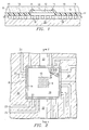
- Figure 1 is a cross-sectional illustration of an integrated circuit package according to the preferred embodiment of the present invention.
- Figure 2 is a plan view of the integrated circuit package according to Figure 1, including a cutaway portion.
- Figure 3 is a cross-sectional illustration of an integrated circuit package according to an alternative preferred embodiment of the present invention.
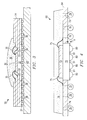
- Figure 4 is a cross-sectional view an integrated circuit package according to another alternative preferred embodiment of the present invention, prior to reflow.
- Figure 5 is a plan view of a solder mask according to the embodiment of the invention of Figure 4.
- Figure 6 is a cross-sectional view of the package of Figure 4, after solder reflow mounting to a circuit board.
- packaged integrated circuit 8 according to a first preferred embodiment of the invention will now be described in detail. While packaged integrated circuit 8 according to this embodiment of the invention is shown in each of Figures 1 and 2 as already attached to system circuit board 20, it is to be understood by those of ordinary skill in the art that packaged integrated circuit 8 according to this embodiment of the invention will often individually manufactured and sold, with the purchaser performing the installation of packaged integrated circuit 8 to system circuit board 20 in a computer or other end equipment.
- the active element of packaged integrated circuit 8 is semiconductor chip 10, which is a solid-state integrated circuit device such as a microprocessor, memory, logic device, analog device or other electronic function implemented in a single-chip integrated circuit, as known in the art. According to this embodiment of the invention, chip 10 is attached on its bottom (inactive) surface to conductive slug 12, mounted within substrate 14.
- Substrate 14 may be a ceramic substrate, printed circuit board, or other similar substrate having conductors 24 thereupon or therewithin (see Figure 2) for carrying electrical signals to and from chip 10, and having an opening or receptacle therein within which conductive slug 12 is mounted.
- Bond wires 15 connect conductors 24 to bond pads on chip 10 in the conventional manner.
- Plated-through vias 19 make connection between conductors 24 on the top surface of substrate 14 and solder balls 18 on the lower surface of substrate 14.
- solder balls 18 are arranged in the conventional ball-grid-array manner, and correspond to lands or other surface conductors 23 (see Figure 2) on the top surface of system circuit board 20 to which packaged integrated circuit 8 is to be mounted.
- Conductive slug 12 is preferably formed of a material with high thermal conductivity, so that heat from chip 10 may be readily conducted therethrough. In addition, if electrical connection is to be made to the body of chip 10, conductive slug 12 is also preferably electrically conductive. The preferred material for conductive slug 12 is believed to be copper, but other materials known in the art to be thermally conductive and, if desired, electrically conductive, may alternatively be used for slug 12.
- Solder balls 18 are also disposed in an array manner beneath and in contact with slug 12, for providing thermal connection between slug 12 and a thermal conductor in system circuit board 20.
- conductive trace 22 is a wide trace on system circuit board 20 that is capable of conducting heat from chip 10 via slug 12 and solder balls 18.
- slug 12 may be connected by solder balls 18 to a ground plane within system circuit board 20. In either case, conductor 22 or the ground plane may be biased to ground or another substrate bias voltage, in which case slug 12 will also provide proper grounding for chip 10.
- packaged integrated circuit 8 begins with the insertion of slug 12 into the corresponding cavity of substrate 14; slug 12 is preferably epoxied into this cavity for mechanical integrity.
- Chip 10 is then mounted to the top surface of slug 12 by conventional die attach techniques, such as a conductive epoxy or eutectic mount.
- Bond wires 15 are then attached between substrate 14 and chip 10 by conventional techniques, such as thermocompression or ultrasonic bonding.
- encapsulant 16 is formed over chip 10 and wires 15 in the conventional manner.
- encapsulate 16 is formed by conventional transfer molding; alternatively, encapsulant 16 may be "globbed" over chip 10 and substrate 14 by dispensation and curing, in the conventional manner.
- Solder balls 18 are formed on the underside of substrate 14 and slug 12, in the conventional manner, for example by way of a solder mask (not shown) on the underside of substrate 14.
- packaged integrated circuit 8 Upon completion of the construction of packaged integrated circuit 8, and any desired electrical testing in packaged form, packaged integrated circuit 8 is ready for mounting to system circuit board 20. Mounting of packaged integrated circuit 8 is preferably done by way of wave soldering or other conventional technique for the surface mounting of BGA packages to circuit boards.
- Figure 3 illustrates, in cross-section, packaged integrated circuit 50 according to a second embodiment of the invention.
- packaged integrated circuit 50 includes chip 30 mounted upon thermally conductive slug 32.
- Slug 32 is disposed within substrate 34, which in this example is a multilayer circuit board including multiple levels of conductors therewithin.
- the multiple levels of conductors in substrate 34 are presented by multiple shells of lands, as indicated by the stepped arrangement near the chip cavity of substrate 34.
- a cutout is provided on the underside of substrate 34, to provide lateral surfaces 33 to which slug 32 may be epoxied or otherwise securely fastened.
- slug 32 includes a smaller portion protruding through substrate 34, to which chip 30 is mounted, with larger exposure on the underside of substrate 34.
- This construction allows for slug 32 to be the proper size for receipt of chip 30 on its top size, providing the maximum area for the arrangement of bond wire lands on substrate 34 with minimum wire length, while maximizing the surface area of thermal conduction on the underside.
- Bond wires 35 electrically connect conductors (not shown) in substrate 34 to pads on the surface of chip 30, for connection to the multiple planes of conductors.
- encapsulant 36 is disposed over the cavity of substrate 34, and thus over chip 30 and wires 35.
- Encapsulant 36 according to this embodiment of the invention is dispensed by way of a syringe or other liquid dispenser, and is then cured in the conventional manner for so-called "chip-on-board" construction.
- Solder balls 38 are attached to lands on the bottom surface of substrate 34. Vias (not shown) are provided within substrate 34 to provide electrical connection to the conductors in the substrate. Solder mask 37 on the underside of substrate 34 assists in defining the location of solder balls 38, during their formation in the conventional manner.
- packaged integrated circuit 50 is attached to system circuit board 40 by way of infrared (IR) solder reflow or other conventional surface mount technology.
- IR infrared
- Those solder balls 38 that are in contact with slug 32 connect to a thermal conductor within system circuit board 40, thus providing a path of relatively low thermal resistance between chip 30 and system circuit board 40 through solder balls 38 and slug 32.
- packaged integrated circuit 60 according to another alternative embodiment of the invention is illustrated in cross-section, prior to its mounting to a printed circuit board.
- packaged circuit 60 includes chip 70 mounted upon thermally conductive slug 72.
- slug 72 is disposed mostly within substrate 74, but has a bottom portion which protrudes from the underside of substrate 74 by a selected distance d; the distance d corresponds to the relative size of solder connections to be formed thereunder relative to those used to make the electrical connections, as will be described in detail hereinbelow.
- Bond wires 75 electrically connect conductors (not shown) in substrate 74 to pads on the surface of chip 70, in the conventional manner; of course, the connection may be made at multiple levels, where substrate 74 includes multiple planes of conductors, as described hereinabove.
- slug 72 may be formed to have stepped portions to maximize thermal conduction while having a reduced chip mount area, as discussed hereinabove relative to Figure 3.
- Bond wires 75 are then attached between substrate 74 and chip 70 by conventional techniques, such as thermocompression or ultrasonic bonding.
- encapsulant 76 is formed over chip 70 and wires 75 in the conventional manner, such as by conventional transfer molding or by dispensing and curing encapsulant 16 thereover.
- Solder balls 78, 80 are next attached to wettable locations, or lands, on the bottom surface of substrate 74 and on the protruding bottom surface of slug 72, respectively.
- vias 79 are provided therewithin to provide electrical connection between the conductors in substrate 74 and solder balls 78; a solder mask (not shown) may be used to define the lands, if the construction of substrate 74 itself does not define the locations at which solder balls 78 are defined.
- the bottom protruding surface of substrate 74 is supplied with solder mask 81 on its underside, having apertures therethrough that define the location of solder balls 80 during their formation.
- Solder mask 81 consists of a photosensitive polymer, applied to, exposed, and developed at the underside of slug 72, in the conventional manner.
- Figure 5 illustrates, in plan view, an example of solder mask 81 as applied to the underside of slug 74, and having apertures 83 therethrough; the scale of apertures 83 to the overall size of slug 74 will, of course, vary with the particular application.
- solder balls 78, 80 to packaged integrated circuit 60 utilizes previously formed solder spheres of the desired diameter.
- Solder spheres are fabricated by conventional techniques, such as atomization of solder, and are generally received by the integrated circuit manufacturer as incoming piece parts. These solder spheres are applied to the bottom of packaged integrated circuit 60 in the conventional manner, by way of a shaker or other fixture having dispensing holes aligned with lands on the bottom of substrate 74 and with apertures 83 in solder mask 81 on the underside of slug 72. The solder spheres are then subjected to reflow temperatures to create solder balls 78, 80 as shown in Figure 4, having a shape defined by the size of wettable surface at the contact locations in combination with the surface tension of the reflowed solder.
- solder balls 78, 80 it is highly desirable and preferable to form solder balls 78, 80 from incoming solder spheres that have a common diameter, such that the same application fixture may be used for packaged integrated circuit 60. It will also be appreciated that the use of differently sized solder spheres to form solder balls 78, 80 would require significantly more complex, and thus costly, assembly equipment, and would also result in more cumbersome inventory management. According to this embodiment of the invention, the different size apertures through solder mask 81 at the protruding bottom surface of slug 74, relative to the size of wettable lands at the bottom of 74, results in solder balls 78, 80 having the same volume, but having radically different shape.
- solder balls 78 will have a nearly spherical shape.
- solder balls 80 having a semi-spherical shape.
- the relative size of the apertures in solder mask 81 at slug 72 to the wettable lands on the bottom surface 74 depends upon the distance d that slug 72 protrudes from the bottom surface of substrate 74. This is because it is highly desirable for the bottom tangent of each of solder balls 78, 80 to be in coplanar with one another; such a relationship enables reliable contact with a printed circuit board after assembly.
- An example of integrated circuit package 60 utilizes solder balls 78, 80 formed from spheres on the order of approximately 0.031 inches in diameter.
- substrate 74 has wettable lands that are on the order of 0.025 inches in diameter; for slug 72 protruding approximately 0.010 inches from the bottom surface of substrate 74, apertures in solder mask 81 that are on the order of 0.035 to 0.040 inches in diameter are contemplated to successfully result in excellent thermal conduction between slug 72 and the circuit board. It is contemplated that similar relative dimensions of protrusion depth to wettable surface size, for a given solder ball size, may be readily calculated for other applications.
- packaged integrated circuit 70 is attached to system circuit board 80 by way of infrared (IR) solder reflow or other conventional surface mount technology.
- IR infrared
- solder leads 80' are formed from solder balls 80, and connect slug 72 to a thermal conductor within system circuit board 82, providing a path of relatively low thermal resistance between chip 70 and system circuit board 80 through solder balls 80' and slug 72.
- solder leads 78' are formed from solder balls 78 to electrically connect lands in substrate 74 to electrical conductors in circuit board 82.
- solder leads 80' have substantially a wider cross-section than do solder leads 78'; the difference in cross-section, of course, arises from the closer proximity of slug 72 to circuit board 82, and from the larger apertures in solder mask 81 relative to lands on substrate 74, given that each of solder balls 78, 80 had substantially the same volume.
- solder leads 80' may also be used to provide electrical connection between packaged integrated circuit 60 and circuit board 82, particularly in providing a solid ground path therebetween.
- vias would be provided through circuit board 82 so that solder leads 80' directly connect chip 70 to a ground plane within circuit board 82.
- the increased width of solder leads 80' thus would provide a low resistance path, both electrically and thermally, between chip 70 (either directly via its substrate or by way of additional wire leads, or both) and the system ground.
- solder leads 80' i.e., the distance between circuit board 82 and the bottom of slug 72
- a typical standoff of solder lead 78' i.e., the distance between circuit board 82 and the bottom of substrate 74
- the volume of solder leads 78', 80' would be equivalent, the reduced standoff of leads 80' will translate to a thickness that, on average, is approximately twice that of leads 78'.
- an integrated circuit package is provided that allows for increased thermal conductivity between the integrated circuit chip and a thermal conductor in the printed circuit board.
- This increased thermal conductivity is obtained while using the same size solder balls for connection as those used for electrical connections, thus easing the solder ball manufacturing process.
- high thermal conductivity is made available for those applications in which the size of thermal conductors in the circuit board is limited.
- an integrated circuit package which has a high thermal conductivity path is provided between the active integrated circuit therewithin and the system circuit board to which the packaged integrated circuit is mounted.
- This enables the advantageous use of the system circuit board thermal conductivity to remove heat from the integrated circuit chip via conduction, and as such is suitable for use in zero-air-flow environments such as notebook-size computers, hand-held computing devices such as PDAs, and the like.
Landscapes
- Engineering & Computer Science (AREA)
- Manufacturing & Machinery (AREA)
- Microelectronics & Electronic Packaging (AREA)
- Electric Connection Of Electric Components To Printed Circuits (AREA)
- Structures For Mounting Electric Components On Printed Circuit Boards (AREA)
Applications Claiming Priority (2)
| Application Number | Priority Date | Filing Date | Title |
|---|---|---|---|
| US08/269,203 US5642261A (en) | 1993-12-20 | 1994-06-30 | Ball-grid-array integrated circuit package with solder-connected thermal conductor |
| US269203 | 2002-10-10 |
Publications (2)
| Publication Number | Publication Date |
|---|---|
| EP0690500A1 true EP0690500A1 (de) | 1996-01-03 |
| EP0690500B1 EP0690500B1 (de) | 2003-02-26 |
Family
ID=23026240
Family Applications (1)
| Application Number | Title | Priority Date | Filing Date |
|---|---|---|---|
| EP95304443A Expired - Lifetime EP0690500B1 (de) | 1994-06-30 | 1995-06-23 | Kugelmatrixgehäuse für integrierte Schaltung mit lötverbundenen thermischen Leiter |
Country Status (4)
| Country | Link |
|---|---|
| US (1) | US5642261A (de) |
| EP (1) | EP0690500B1 (de) |
| JP (1) | JPH0855933A (de) |
| DE (1) | DE69529706T2 (de) |
Cited By (7)
| Publication number | Priority date | Publication date | Assignee | Title |
|---|---|---|---|---|
| EP0771029A3 (de) * | 1995-10-24 | 1997-07-30 | Oki Electric Ind Co Ltd | Halbleitereinrichtung mit verbesserter Struktur zur Vermeidung von Rissen und Herstellungsverfahren |
| GB2297652B (en) * | 1995-02-03 | 1999-03-31 | Plessey Semiconductors Ltd | Microchip module assemblies |
| US7543377B2 (en) | 1996-03-28 | 2009-06-09 | Intel Corporation | Perimeter matrix ball grid array circuit package with a populated center |
| EP2899752A1 (de) * | 2014-01-27 | 2015-07-29 | MediaTek, Inc | Struktur und Formungsverfahren einer Chipgehäusestruktur |
| GB2525585A (en) * | 2014-03-20 | 2015-11-04 | Micross Components Ltd | Leadless chip carrier |
| WO2015193153A1 (en) * | 2014-06-18 | 2015-12-23 | Element Six Technologies Limited | An electronic device component with an integral diamond heat spreader |
| US12127334B2 (en) | 2019-02-01 | 2024-10-22 | Dis Tech America, Llc | Maintaining the shape of a circuit board |
Families Citing this family (126)
| Publication number | Priority date | Publication date | Assignee | Title |
|---|---|---|---|---|
| US6734545B1 (en) * | 1995-11-29 | 2004-05-11 | Hitachi, Ltd. | BGA type semiconductor device and electronic equipment using the same |
| US6861290B1 (en) * | 1995-12-19 | 2005-03-01 | Micron Technology, Inc. | Flip-chip adaptor package for bare die |
| US6730991B1 (en) * | 1996-06-11 | 2004-05-04 | Raytheon Company | Integrated circuit chip package |
| US5790377A (en) * | 1996-09-12 | 1998-08-04 | Packard Hughes Interconnect Company | Integral copper column with solder bump flip chip |
| US5831826A (en) * | 1996-09-20 | 1998-11-03 | Motorola, Inc. | Heat transfer apparatus suitable for use in a circuit board assembly |
| JP2975979B2 (ja) * | 1996-12-30 | 1999-11-10 | アナムインダストリアル株式会社 | ボールグリッドアレイ半導体パッケージ用可撓性回路基板 |
| US6249046B1 (en) * | 1997-02-13 | 2001-06-19 | Seiko Epson Corporation | Semiconductor device and method for manufacturing and mounting thereof, and circuit board mounted with the semiconductor device |
| US6829149B1 (en) * | 1997-08-18 | 2004-12-07 | International Business Machines Corporation | Placement of sacrificial solder balls underneath the PBGA substrate |
| US6300678B1 (en) | 1997-10-03 | 2001-10-09 | Fujitsu Limited | I/O pin having solder dam for connecting substrates |
| DE19750306A1 (de) * | 1997-11-13 | 1999-05-20 | Bosch Gmbh Robert | Elektronisches Steuergerät |
| US6376908B1 (en) | 1997-12-10 | 2002-04-23 | Mitsubishi Gas Chemical Company, Inc. | Semiconductor plastic package and process for the production thereof |
| US6072233A (en) | 1998-05-04 | 2000-06-06 | Micron Technology, Inc. | Stackable ball grid array package |
| USRE43112E1 (en) | 1998-05-04 | 2012-01-17 | Round Rock Research, Llc | Stackable ball grid array package |
| US6011696A (en) * | 1998-05-28 | 2000-01-04 | Intel Corporation | Cartridge and an enclosure for a semiconductor package |
| US6196439B1 (en) | 1998-05-29 | 2001-03-06 | International Business Machines Corporation | Method and apparatus for μBGA removal and reattach |
| KR100271656B1 (ko) | 1998-05-30 | 2000-11-15 | 김영환 | 비지에이 반도체 패키지 및 그 제조방법 |
| JPH11345905A (ja) | 1998-06-02 | 1999-12-14 | Mitsubishi Electric Corp | 半導体装置 |
| SE512710C2 (sv) * | 1998-07-08 | 2000-05-02 | Ericsson Telefon Ab L M | Kapsel för högeffekttransistorchip för höga frekvenser innefattande en elektriskt och termiskt ledande fläns |
| JP3602968B2 (ja) * | 1998-08-18 | 2004-12-15 | 沖電気工業株式会社 | 半導体装置およびその基板接続構造 |
| US6674163B1 (en) * | 1998-08-18 | 2004-01-06 | Oki Electric Industry Co., Ltd. | Package structure for a semiconductor device |
| US6121576A (en) | 1998-09-02 | 2000-09-19 | Micron Technology, Inc. | Method and process of contact to a heat softened solder ball array |
| US6251219B1 (en) | 1998-09-17 | 2001-06-26 | Intermedics Inc. | Method and apparatus for use in assembling electronic devices |
| US6505665B1 (en) | 1998-09-17 | 2003-01-14 | Intermedics, Inc. | Method and apparatus for use in assembling electronic devices |
| KR100302593B1 (ko) | 1998-10-24 | 2001-09-22 | 김영환 | 반도체패키지및그제조방법 |
| US6154364A (en) * | 1998-11-19 | 2000-11-28 | Delco Electronics Corp. | Circuit board assembly with IC device mounted thereto |
| US6844253B2 (en) | 1999-02-19 | 2005-01-18 | Micron Technology, Inc. | Selective deposition of solder ball contacts |
| US6419517B1 (en) * | 1999-02-26 | 2002-07-16 | Micron Technology, Inc. | Apparatus and method for packaging circuits |
| TW413874B (en) | 1999-04-12 | 2000-12-01 | Siliconware Precision Industries Co Ltd | BGA semiconductor package having exposed heat dissipation layer and its manufacturing method |
| US6396143B1 (en) * | 1999-04-30 | 2002-05-28 | Mitsubishi Gas Chemical Company, Inc. | Ball grid array type printed wiring board having exellent heat diffusibility and printed wiring board |
| US6337228B1 (en) | 1999-05-12 | 2002-01-08 | Amkor Technology, Inc. | Low-cost printed circuit board with integral heat sink for semiconductor package |
| US6196002B1 (en) * | 1999-06-24 | 2001-03-06 | Advanced Micro Devices, Inc. | Ball grid array package having thermoelectric cooler |
| US6442039B1 (en) | 1999-12-03 | 2002-08-27 | Delphi Technologies, Inc. | Metallic microstructure springs and method of making same |
| US6435396B1 (en) * | 2000-04-10 | 2002-08-20 | Micron Technology, Inc. | Print head for ejecting liquid droplets |
| US6878396B2 (en) * | 2000-04-10 | 2005-04-12 | Micron Technology, Inc. | Micro C-4 semiconductor die and method for depositing connection sites thereon |
| TW462121B (en) * | 2000-09-19 | 2001-11-01 | Siliconware Precision Industries Co Ltd | Heat sink type ball grid array package |
| JP3634735B2 (ja) * | 2000-10-05 | 2005-03-30 | 三洋電機株式会社 | 半導体装置および半導体モジュール |
| TW497371B (en) * | 2000-10-05 | 2002-08-01 | Sanyo Electric Co | Semiconductor device and semiconductor module |
| CN1184684C (zh) * | 2000-10-05 | 2005-01-12 | 三洋电机株式会社 | 半导体装置和半导体模块 |
| US6960824B1 (en) * | 2000-11-15 | 2005-11-01 | Skyworks Solutions, Inc. | Structure and method for fabrication of a leadless chip carrier |
| US6882042B2 (en) * | 2000-12-01 | 2005-04-19 | Broadcom Corporation | Thermally and electrically enhanced ball grid array packaging |
| US7132744B2 (en) * | 2000-12-22 | 2006-11-07 | Broadcom Corporation | Enhanced die-up ball grid array packages and method for making the same |
| US20020079572A1 (en) | 2000-12-22 | 2002-06-27 | Khan Reza-Ur Rahman | Enhanced die-up ball grid array and method for making the same |
| US7161239B2 (en) * | 2000-12-22 | 2007-01-09 | Broadcom Corporation | Ball grid array package enhanced with a thermal and electrical connector |
| US6906414B2 (en) * | 2000-12-22 | 2005-06-14 | Broadcom Corporation | Ball grid array package with patterned stiffener layer |
| US6396699B1 (en) * | 2001-01-19 | 2002-05-28 | Lsi Logic Corporation | Heat sink with chip die EMC ground interconnect |
| US6853070B2 (en) | 2001-02-15 | 2005-02-08 | Broadcom Corporation | Die-down ball grid array package with die-attached heat spreader and method for making the same |
| TW495943B (en) * | 2001-04-18 | 2002-07-21 | Siliconware Precision Industries Co Ltd | Semiconductor package article with heat sink structure and its manufacture method |
| US7259448B2 (en) | 2001-05-07 | 2007-08-21 | Broadcom Corporation | Die-up ball grid array package with a heat spreader and method for making the same |
| US6790710B2 (en) | 2002-01-31 | 2004-09-14 | Asat Limited | Method of manufacturing an integrated circuit package |
| US7176506B2 (en) * | 2001-08-28 | 2007-02-13 | Tessera, Inc. | High frequency chip packages with connecting elements |
| US6856007B2 (en) * | 2001-08-28 | 2005-02-15 | Tessera, Inc. | High-frequency chip packages |
| US6657296B2 (en) | 2001-09-25 | 2003-12-02 | Siliconware Precision Industries Co., Ltd. | Semicondctor package |
| US7335995B2 (en) * | 2001-10-09 | 2008-02-26 | Tessera, Inc. | Microelectronic assembly having array including passive elements and interconnects |
| WO2003032370A2 (en) * | 2001-10-09 | 2003-04-17 | Tessera, Inc. | Stacked packages |
| US6977440B2 (en) * | 2001-10-09 | 2005-12-20 | Tessera, Inc. | Stacked packages |
| US6787895B1 (en) * | 2001-12-07 | 2004-09-07 | Skyworks Solutions, Inc. | Leadless chip carrier for reduced thermal resistance |
| US6879039B2 (en) | 2001-12-18 | 2005-04-12 | Broadcom Corporation | Ball grid array package substrates and method of making the same |
| US6825108B2 (en) * | 2002-02-01 | 2004-11-30 | Broadcom Corporation | Ball grid array package fabrication with IC die support structures |
| US7245500B2 (en) * | 2002-02-01 | 2007-07-17 | Broadcom Corporation | Ball grid array package with stepped stiffener layer |
| US6861750B2 (en) * | 2002-02-01 | 2005-03-01 | Broadcom Corporation | Ball grid array package with multiple interposers |
| US7550845B2 (en) | 2002-02-01 | 2009-06-23 | Broadcom Corporation | Ball grid array package with separated stiffener layer |
| US6876553B2 (en) * | 2002-03-21 | 2005-04-05 | Broadcom Corporation | Enhanced die-up ball grid array package with two substrates |
| US7196415B2 (en) | 2002-03-22 | 2007-03-27 | Broadcom Corporation | Low voltage drop and high thermal performance ball grid array package |
| US6765288B2 (en) * | 2002-08-05 | 2004-07-20 | Tessera, Inc. | Microelectronic adaptors, assemblies and methods |
| WO2004017399A1 (en) * | 2002-08-16 | 2004-02-26 | Tessera, Inc. | Microelectronic packages with self-aligning features |
| US7294928B2 (en) * | 2002-09-06 | 2007-11-13 | Tessera, Inc. | Components, methods and assemblies for stacked packages |
| US7071547B2 (en) * | 2002-09-11 | 2006-07-04 | Tessera, Inc. | Assemblies having stacked semiconductor chips and methods of making same |
| CN1711636A (zh) * | 2002-10-11 | 2005-12-21 | 德塞拉股份有限公司 | 用于多芯片封装的元件、方法和组件 |
| US6876088B2 (en) | 2003-01-16 | 2005-04-05 | International Business Machines Corporation | Flex-based IC package construction employing a balanced lamination |
| US7253510B2 (en) * | 2003-01-16 | 2007-08-07 | International Business Machines Corporation | Ball grid array package construction with raised solder ball pads |
| US6867121B2 (en) * | 2003-01-16 | 2005-03-15 | International Business Machines Corporation | Method of apparatus for interconnecting a relatively fine pitch circuit layer and adjacent power plane(s) in a laminated construction |
| US7754537B2 (en) * | 2003-02-25 | 2010-07-13 | Tessera, Inc. | Manufacture of mountable capped chips |
| KR100548554B1 (ko) * | 2003-03-04 | 2006-02-02 | 주식회사 하이닉스반도체 | 테스트 비이클 볼 그리드 어레이 패키지 |
| TW200419752A (en) * | 2003-03-18 | 2004-10-01 | United Test Ct Inc | Semiconductor package with heat sink |
| JP4096774B2 (ja) * | 2003-03-24 | 2008-06-04 | セイコーエプソン株式会社 | 半導体装置、電子デバイス、電子機器、半導体装置の製造方法及び電子デバイスの製造方法 |
| US7126210B2 (en) * | 2003-04-02 | 2006-10-24 | Stmicroelectronics, Inc. | System and method for venting pressure from an integrated circuit package sealed with a lid |
| US20040245617A1 (en) * | 2003-05-06 | 2004-12-09 | Tessera, Inc. | Dense multichip module |
| US20040245624A1 (en) * | 2003-06-03 | 2004-12-09 | Swanson Leland S. | Using solder balls of multiple sizes to couple one or more semiconductor structures to an electrical device |
| US6972480B2 (en) | 2003-06-16 | 2005-12-06 | Shellcase Ltd. | Methods and apparatus for packaging integrated circuit devices |
| US7347349B2 (en) * | 2003-06-24 | 2008-03-25 | Micron Technology, Inc. | Apparatus and method for printing micro metal structures |
| WO2005004195A2 (en) | 2003-07-03 | 2005-01-13 | Shellcase Ltd. | Method and apparatus for packaging integrated circuit devices |
| US6809260B1 (en) * | 2003-09-22 | 2004-10-26 | Intel Corporation | Apparatus and method for an integrated high-performance electrical interconnect |
| US7224056B2 (en) | 2003-09-26 | 2007-05-29 | Tessera, Inc. | Back-face and edge interconnects for lidded package |
| US7084500B2 (en) * | 2003-10-29 | 2006-08-01 | Texas Instruments Incorporated | Semiconductor circuit with multiple contact sizes |
| US7061121B2 (en) | 2003-11-12 | 2006-06-13 | Tessera, Inc. | Stacked microelectronic assemblies with central contacts |
| US20050258534A1 (en) * | 2004-05-24 | 2005-11-24 | Nokia Corporation | Arrangement for receiving an electronic component capable of high power operation |
| US7432586B2 (en) | 2004-06-21 | 2008-10-07 | Broadcom Corporation | Apparatus and method for thermal and electromagnetic interference (EMI) shielding enhancement in die-up array packages |
| US7411281B2 (en) * | 2004-06-21 | 2008-08-12 | Broadcom Corporation | Integrated circuit device package having both wire bond and flip-chip interconnections and method of making the same |
| US7482686B2 (en) * | 2004-06-21 | 2009-01-27 | Braodcom Corporation | Multipiece apparatus for thermal and electromagnetic interference (EMI) shielding enhancement in die-up array packages and method of making the same |
| KR100630690B1 (ko) * | 2004-07-08 | 2006-10-02 | 삼성전자주식회사 | 열 소산 경로를 구비한 멀티 칩 패키지 |
| US7786591B2 (en) * | 2004-09-29 | 2010-08-31 | Broadcom Corporation | Die down ball grid array package |
| US8143095B2 (en) | 2005-03-22 | 2012-03-27 | Tessera, Inc. | Sequential fabrication of vertical conductive interconnects in capped chips |
| JP4408832B2 (ja) * | 2005-05-20 | 2010-02-03 | Necエレクトロニクス株式会社 | 半導体装置 |
| JP4667154B2 (ja) * | 2005-08-03 | 2011-04-06 | 京セラ株式会社 | 配線基板、電気素子装置並びに複合基板 |
| US20070090517A1 (en) * | 2005-10-05 | 2007-04-26 | Moon Sung-Won | Stacked die package with thermally conductive block embedded in substrate |
| US7582951B2 (en) * | 2005-10-20 | 2009-09-01 | Broadcom Corporation | Methods and apparatus for improved thermal performance and electromagnetic interference (EMI) shielding in leadframe integrated circuit (IC) packages |
| US7936062B2 (en) | 2006-01-23 | 2011-05-03 | Tessera Technologies Ireland Limited | Wafer level chip packaging |
| US7714453B2 (en) * | 2006-05-12 | 2010-05-11 | Broadcom Corporation | Interconnect structure and formation for package stacking of molded plastic area array package |
| US8183680B2 (en) * | 2006-05-16 | 2012-05-22 | Broadcom Corporation | No-lead IC packages having integrated heat spreader for electromagnetic interference (EMI) shielding and thermal enhancement |
| US7808087B2 (en) | 2006-06-01 | 2010-10-05 | Broadcom Corporation | Leadframe IC packages having top and bottom integrated heat spreaders |
| US20080083981A1 (en) * | 2006-06-07 | 2008-04-10 | Romig Matthew D | Thermally Enhanced BGA Packages and Methods |
| US8581381B2 (en) | 2006-06-20 | 2013-11-12 | Broadcom Corporation | Integrated circuit (IC) package stacking and IC packages formed by same |
| US7545029B2 (en) * | 2006-08-18 | 2009-06-09 | Tessera, Inc. | Stack microelectronic assemblies |
| US7554194B2 (en) * | 2006-11-08 | 2009-06-30 | Amkor Technology, Inc. | Thermally enhanced semiconductor package |
| US7486517B2 (en) * | 2006-12-20 | 2009-02-03 | Nokia Corporation | Hand-held portable electronic device having a heat spreader |
| US8604605B2 (en) | 2007-01-05 | 2013-12-10 | Invensas Corp. | Microelectronic assembly with multi-layer support structure |
| US8183687B2 (en) * | 2007-02-16 | 2012-05-22 | Broadcom Corporation | Interposer for die stacking in semiconductor packages and the method of making the same |
| US7872335B2 (en) * | 2007-06-08 | 2011-01-18 | Broadcom Corporation | Lead frame-BGA package with enhanced thermal performance and I/O counts |
| US7479406B1 (en) * | 2008-03-14 | 2009-01-20 | International Business Machines Corporation | Bottom heatslug EPBGA for high thermal performance |
| US8076786B2 (en) * | 2008-07-11 | 2011-12-13 | Advanced Semiconductor Engineering, Inc. | Semiconductor package and method for packaging a semiconductor package |
| US20100019374A1 (en) * | 2008-07-25 | 2010-01-28 | Stmicroelectronics, Inc. | Ball grid array package |
| US7989950B2 (en) | 2008-08-14 | 2011-08-02 | Stats Chippac Ltd. | Integrated circuit packaging system having a cavity |
| US8823160B2 (en) * | 2008-08-22 | 2014-09-02 | Stats Chippac Ltd. | Integrated circuit package system having cavity |
| JP4789997B2 (ja) * | 2008-11-20 | 2011-10-12 | 三菱電機株式会社 | 電子基板装置 |
| US8611636B1 (en) | 2009-01-05 | 2013-12-17 | Cognex Corporation | High speed method of aligning components having a plurality of non-uniformly spaced features |
| US8547709B2 (en) * | 2010-02-12 | 2013-10-01 | Cyntec Co. Ltd. | Electronic system with a composite substrate |
| EP2362431B1 (de) * | 2010-02-25 | 2018-01-10 | Saint-Augustin Canada Electric Inc. | Solarzellenanordnung |
| US8248803B2 (en) * | 2010-03-31 | 2012-08-21 | Hong Kong Applied Science and Technology Research Institute Company Limited | Semiconductor package and method of manufacturing the same |
| US9099318B2 (en) * | 2010-10-15 | 2015-08-04 | Taiwan Semiconductor Manufacturing Company, Ltd. | Semiconductor chip having different pad width to UBM width ratios and method of manufacturing the same |
| US20130249073A1 (en) * | 2012-03-22 | 2013-09-26 | Hsin Hung Chen | Integrated circuit packaging system with support structure and method of manufacture thereof |
| US9237659B2 (en) * | 2012-09-28 | 2016-01-12 | Intel Corporation | BGA structure using CTF balls in high stress regions |
| US8969191B2 (en) | 2013-07-16 | 2015-03-03 | Taiwan Semiconductor Manufacturing Co., Ltd. | Mechanisms for forming package structure |
| JP2016025143A (ja) * | 2014-07-17 | 2016-02-08 | イビデン株式会社 | 回路基板及びその製造方法 |
| JP2016149475A (ja) * | 2015-02-13 | 2016-08-18 | イビデン株式会社 | 回路基板及びその製造方法 |
| FR3050073B1 (fr) * | 2016-04-12 | 2018-05-04 | Mbda France | Systeme electronique pourvu d'une pluralite de fonctions electroniques interconnectees |
| US10269678B1 (en) * | 2017-12-05 | 2019-04-23 | Nxp Usa, Inc. | Microelectronic components having integrated heat dissipation posts, systems including the same, and methods for the fabrication thereof |
Citations (6)
| Publication number | Priority date | Publication date | Assignee | Title |
|---|---|---|---|---|
| EP0333237A2 (de) * | 1984-05-18 | 1989-09-20 | BRITISH TELECOMMUNICATIONS public limited company | Integrierter Schaltungschipträger |
| EP0376100A2 (de) * | 1988-12-24 | 1990-07-04 | Alcatel SEL Aktiengesellschaft | Verfahren und Leiterplatte zum Montieren eines Halbleiter-Bauelements |
| US5216278A (en) * | 1990-12-04 | 1993-06-01 | Motorola, Inc. | Semiconductor device having a pad array carrier package |
| DE9308842U1 (de) * | 1993-06-14 | 1993-07-22 | Blaupunkt-Werke Gmbh, 31139 Hildesheim | Elektrische Baugruppe |
| US5285352A (en) * | 1992-07-15 | 1994-02-08 | Motorola, Inc. | Pad array semiconductor device with thermal conductor and process for making the same |
| EP0660399A2 (de) * | 1993-12-20 | 1995-06-28 | STMicroelectronics, Inc. | Kugelrastergehäuse für integrierte Schaltung mit Wärmeleitung |
Family Cites Families (6)
| Publication number | Priority date | Publication date | Assignee | Title |
|---|---|---|---|---|
| JP2660295B2 (ja) * | 1988-08-24 | 1997-10-08 | イビデン株式会社 | 電子部品搭載用基板 |
| JPH03198368A (ja) * | 1989-12-26 | 1991-08-29 | Nec Corp | 半導体装置 |
| US5172301A (en) * | 1991-10-08 | 1992-12-15 | Lsi Logic Corporation | Heatsink for board-mounted semiconductor devices and semiconductor device assembly employing same |
| CA2089435C (en) * | 1992-02-14 | 1997-12-09 | Kenzi Kobayashi | Semiconductor device |
| US5222014A (en) * | 1992-03-02 | 1993-06-22 | Motorola, Inc. | Three-dimensional multi-chip pad array carrier |
| US5291062A (en) * | 1993-03-01 | 1994-03-01 | Motorola, Inc. | Area array semiconductor device having a lid with functional contacts |
-
1994
- 1994-06-30 US US08/269,203 patent/US5642261A/en not_active Expired - Lifetime
-
1995
- 1995-06-23 EP EP95304443A patent/EP0690500B1/de not_active Expired - Lifetime
- 1995-06-23 DE DE69529706T patent/DE69529706T2/de not_active Expired - Fee Related
- 1995-06-30 JP JP7165936A patent/JPH0855933A/ja active Pending
Patent Citations (6)
| Publication number | Priority date | Publication date | Assignee | Title |
|---|---|---|---|---|
| EP0333237A2 (de) * | 1984-05-18 | 1989-09-20 | BRITISH TELECOMMUNICATIONS public limited company | Integrierter Schaltungschipträger |
| EP0376100A2 (de) * | 1988-12-24 | 1990-07-04 | Alcatel SEL Aktiengesellschaft | Verfahren und Leiterplatte zum Montieren eines Halbleiter-Bauelements |
| US5216278A (en) * | 1990-12-04 | 1993-06-01 | Motorola, Inc. | Semiconductor device having a pad array carrier package |
| US5285352A (en) * | 1992-07-15 | 1994-02-08 | Motorola, Inc. | Pad array semiconductor device with thermal conductor and process for making the same |
| DE9308842U1 (de) * | 1993-06-14 | 1993-07-22 | Blaupunkt-Werke Gmbh, 31139 Hildesheim | Elektrische Baugruppe |
| EP0660399A2 (de) * | 1993-12-20 | 1995-06-28 | STMicroelectronics, Inc. | Kugelrastergehäuse für integrierte Schaltung mit Wärmeleitung |
Non-Patent Citations (1)
| Title |
|---|
| T. T. LEE: "A Low Cost Bumped Thermal Test Chip Assembly", MOTOROLA TECHNICAL DEVELOPMENTS, vol. 18, SCHAUMBURG, ILLINOIS US, pages 64 - 66 * |
Cited By (15)
| Publication number | Priority date | Publication date | Assignee | Title |
|---|---|---|---|---|
| GB2297652B (en) * | 1995-02-03 | 1999-03-31 | Plessey Semiconductors Ltd | Microchip module assemblies |
| EP0771029A3 (de) * | 1995-10-24 | 1997-07-30 | Oki Electric Ind Co Ltd | Halbleitereinrichtung mit verbesserter Struktur zur Vermeidung von Rissen und Herstellungsverfahren |
| US5864174A (en) * | 1995-10-24 | 1999-01-26 | Oki Electric Industry Co., Ltd. | Semiconductor device having a die pad structure for preventing cracks in a molding resin |
| US6177725B1 (en) | 1995-10-24 | 2001-01-23 | Oki Electric Industry Co., Ltd. | Semiconductor device having an improved structure for preventing cracks, improved small-sized semiconductor and method of manufacturing the same |
| US6459145B1 (en) | 1995-10-24 | 2002-10-01 | Oki Electric Industry Co., Ltd. | Semiconductor device having an improved structure for preventing cracks, and improved small-sized semiconductor |
| US6569755B2 (en) | 1995-10-24 | 2003-05-27 | Oki Electric Industry Co., Ltd. | Semiconductor device having an improved structure for preventing cracks, improved small sized semiconductor and method of manufacturing the same |
| US7543377B2 (en) | 1996-03-28 | 2009-06-09 | Intel Corporation | Perimeter matrix ball grid array circuit package with a populated center |
| EP2899752A1 (de) * | 2014-01-27 | 2015-07-29 | MediaTek, Inc | Struktur und Formungsverfahren einer Chipgehäusestruktur |
| US10431564B2 (en) | 2014-01-27 | 2019-10-01 | Mediatek Inc. | Structure and formation method of chip package structure |
| GB2525585A (en) * | 2014-03-20 | 2015-11-04 | Micross Components Ltd | Leadless chip carrier |
| US9589873B2 (en) | 2014-03-20 | 2017-03-07 | Micross Components Limited | Leadless chip carrier |
| GB2525585B (en) * | 2014-03-20 | 2018-10-03 | Micross Components Ltd | Leadless chip carrier |
| WO2015193153A1 (en) * | 2014-06-18 | 2015-12-23 | Element Six Technologies Limited | An electronic device component with an integral diamond heat spreader |
| US10366936B2 (en) | 2014-06-18 | 2019-07-30 | Element Six Technologies Limited | Electronic device component with an integral diamond heat spreader |
| US12127334B2 (en) | 2019-02-01 | 2024-10-22 | Dis Tech America, Llc | Maintaining the shape of a circuit board |
Also Published As
| Publication number | Publication date |
|---|---|
| EP0690500B1 (de) | 2003-02-26 |
| JPH0855933A (ja) | 1996-02-27 |
| DE69529706T2 (de) | 2003-11-06 |
| US5642261A (en) | 1997-06-24 |
| DE69529706D1 (de) | 2003-04-03 |
Similar Documents
| Publication | Publication Date | Title |
|---|---|---|
| US5642261A (en) | Ball-grid-array integrated circuit package with solder-connected thermal conductor | |
| US5991156A (en) | Ball grid array integrated circuit package with high thermal conductivity | |
| KR100694739B1 (ko) | 다수의 전원/접지면을 갖는 볼 그리드 어레이 패키지 | |
| JP4476482B2 (ja) | ロープロファイルボールグリッドアレイ半導体パッケージ、集積回路、印刷回路板、プロセサシステム、ロープロファイルボールグリッドアレイ半導体パッケージを製造する方法、および、半導体ダイを搭載する方法 | |
| US6146921A (en) | Cavity mold cap BGA package with post mold thermally conductive epoxy attach heat sink | |
| US5977626A (en) | Thermally and electrically enhanced PBGA package | |
| US5291062A (en) | Area array semiconductor device having a lid with functional contacts | |
| US5973393A (en) | Apparatus and method for stackable molded lead frame ball grid array packaging of integrated circuits | |
| US6507107B2 (en) | Semiconductor/printed circuit board assembly | |
| US5302849A (en) | Plastic and grid array semiconductor device and method for making the same | |
| US7400032B2 (en) | Module assembly for stacked BGA packages | |
| US6449159B1 (en) | Semiconductor module with imbedded heat spreader | |
| KR0169820B1 (ko) | 금속 회로 기판을 갖는 칩 스케일 패키지 | |
| US20010001505A1 (en) | Tape ball grid array with interconnected ground plane | |
| US6894229B1 (en) | Mechanically enhanced package and method of making same | |
| JPH09153565A (ja) | ヒートシンク付きボールグリッドアレーパッケージ | |
| US5949651A (en) | Quad flat pack integrated circuit package | |
| KR100386018B1 (ko) | 스택형반도체디바이스패키지 | |
| US6396699B1 (en) | Heat sink with chip die EMC ground interconnect | |
| KR101096330B1 (ko) | 반도체 장치용 패키지 | |
| JP3148718B2 (ja) | 熱的及び電気的に増強された半導体パッケージ | |
| EP0676806B1 (de) | Verpackung eines BGA-integrierten Schaltkreises mit hoher thermischer Leitfähigkeit | |
| KR100230189B1 (ko) | 볼 그리드 어레이 반도체 패키지 | |
| US6963129B1 (en) | Multi-chip package having a contiguous heat spreader assembly | |
| KR100230919B1 (ko) | 반도체 패키지 |
Legal Events
| Date | Code | Title | Description |
|---|---|---|---|
| PUAI | Public reference made under article 153(3) epc to a published international application that has entered the european phase |
Free format text: ORIGINAL CODE: 0009012 |
|
| AK | Designated contracting states |
Kind code of ref document: A1 Designated state(s): DE FR GB IT |
|
| K1C1 | Correction of patent application (title page) published |
Effective date: 19960103 |
|
| 17P | Request for examination filed |
Effective date: 19960627 |
|
| RAP3 | Party data changed (applicant data changed or rights of an application transferred) |
Owner name: STMICROELECTRONICS, INC. |
|
| 17Q | First examination report despatched |
Effective date: 20000124 |
|
| GRAH | Despatch of communication of intention to grant a patent |
Free format text: ORIGINAL CODE: EPIDOS IGRA |
|
| GRAH | Despatch of communication of intention to grant a patent |
Free format text: ORIGINAL CODE: EPIDOS IGRA |
|
| GRAA | (expected) grant |
Free format text: ORIGINAL CODE: 0009210 |
|
| AK | Designated contracting states |
Designated state(s): DE FR GB IT |
|
| PG25 | Lapsed in a contracting state [announced via postgrant information from national office to epo] |
Ref country code: IT Free format text: LAPSE BECAUSE OF FAILURE TO SUBMIT A TRANSLATION OF THE DESCRIPTION OR TO PAY THE FEE WITHIN THE PRE;WARNING: LAPSES OF ITALIAN PATENTS WITH EFFECTIVE DATE BEFORE 2007 MAY HAVE OCCURRED AT ANY TIME BEFORE 2007. THE CORRECT EFFECTIVE DATE MAY BE DIFFERENT FROM THE ONE RECORDED.SCRIBED TIME-LIMIT Effective date: 20030226 |
|
| REG | Reference to a national code |
Ref country code: GB Ref legal event code: FG4D |
|
| REF | Corresponds to: |
Ref document number: 69529706 Country of ref document: DE Date of ref document: 20030403 Kind code of ref document: P |
|
| ET | Fr: translation filed | ||
| PGFP | Annual fee paid to national office [announced via postgrant information from national office to epo] |
Ref country code: DE Payment date: 20031120 Year of fee payment: 9 |
|
| PLBE | No opposition filed within time limit |
Free format text: ORIGINAL CODE: 0009261 |
|
| STAA | Information on the status of an ep patent application or granted ep patent |
Free format text: STATUS: NO OPPOSITION FILED WITHIN TIME LIMIT |
|
| 26N | No opposition filed |
Effective date: 20031127 |
|
| PG25 | Lapsed in a contracting state [announced via postgrant information from national office to epo] |
Ref country code: DE Free format text: LAPSE BECAUSE OF NON-PAYMENT OF DUE FEES Effective date: 20050101 |
|
| PGFP | Annual fee paid to national office [announced via postgrant information from national office to epo] |
Ref country code: FR Payment date: 20060608 Year of fee payment: 12 |
|
| PGFP | Annual fee paid to national office [announced via postgrant information from national office to epo] |
Ref country code: GB Payment date: 20060621 Year of fee payment: 12 |
|
| GBPC | Gb: european patent ceased through non-payment of renewal fee |
Effective date: 20070623 |
|
| REG | Reference to a national code |
Ref country code: FR Ref legal event code: ST Effective date: 20080229 |
|
| PG25 | Lapsed in a contracting state [announced via postgrant information from national office to epo] |
Ref country code: GB Free format text: LAPSE BECAUSE OF NON-PAYMENT OF DUE FEES Effective date: 20070623 |
|
| PG25 | Lapsed in a contracting state [announced via postgrant information from national office to epo] |
Ref country code: FR Free format text: LAPSE BECAUSE OF NON-PAYMENT OF DUE FEES Effective date: 20070702 |