EP0693782A1 - Procédé pour la réduction de l'effet d'antenne pendant la fabrication - Google Patents
Procédé pour la réduction de l'effet d'antenne pendant la fabrication Download PDFInfo
- Publication number
- EP0693782A1 EP0693782A1 EP94305121A EP94305121A EP0693782A1 EP 0693782 A1 EP0693782 A1 EP 0693782A1 EP 94305121 A EP94305121 A EP 94305121A EP 94305121 A EP94305121 A EP 94305121A EP 0693782 A1 EP0693782 A1 EP 0693782A1
- Authority
- EP
- European Patent Office
- Prior art keywords
- metal layer
- layer
- metal
- forming
- contact pad
- Prior art date
- Legal status (The legal status is an assumption and is not a legal conclusion. Google has not performed a legal analysis and makes no representation as to the accuracy of the status listed.)
- Granted
Links
Images


Classifications
-
- H—ELECTRICITY
- H10—SEMICONDUCTOR DEVICES; ELECTRIC SOLID-STATE DEVICES NOT OTHERWISE PROVIDED FOR
- H10W—GENERIC PACKAGES, INTERCONNECTIONS, CONNECTORS OR OTHER CONSTRUCTIONAL DETAILS OF DEVICES COVERED BY CLASS H10
- H10W72/00—Interconnections or connectors in packages
- H10W72/01—Manufacture or treatment
- H10W72/019—Manufacture or treatment of bond pads
-
- H—ELECTRICITY
- H10—SEMICONDUCTOR DEVICES; ELECTRIC SOLID-STATE DEVICES NOT OTHERWISE PROVIDED FOR
- H10D—INORGANIC ELECTRIC SEMICONDUCTOR DEVICES
- H10D89/00—Aspects of integrated devices not covered by groups H10D84/00 - H10D88/00
- H10D89/60—Integrated devices comprising arrangements for electrical or thermal protection, e.g. protection circuits against electrostatic discharge [ESD]
- H10D89/601—Integrated devices comprising arrangements for electrical or thermal protection, e.g. protection circuits against electrostatic discharge [ESD] for devices having insulated gate electrodes, e.g. for IGFETs or IGBTs
-
- H—ELECTRICITY
- H10—SEMICONDUCTOR DEVICES; ELECTRIC SOLID-STATE DEVICES NOT OTHERWISE PROVIDED FOR
- H10W—GENERIC PACKAGES, INTERCONNECTIONS, CONNECTORS OR OTHER CONSTRUCTIONAL DETAILS OF DEVICES COVERED BY CLASS H10
- H10W72/00—Interconnections or connectors in packages
- H10W72/90—Bond pads, in general
- H10W72/931—Shapes of bond pads
- H10W72/932—Plan-view shape, i.e. in top view
-
- H—ELECTRICITY
- H10—SEMICONDUCTOR DEVICES; ELECTRIC SOLID-STATE DEVICES NOT OTHERWISE PROVIDED FOR
- H10W—GENERIC PACKAGES, INTERCONNECTIONS, CONNECTORS OR OTHER CONSTRUCTIONAL DETAILS OF DEVICES COVERED BY CLASS H10
- H10W72/00—Interconnections or connectors in packages
- H10W72/90—Bond pads, in general
- H10W72/951—Materials of bond pads
-
- H—ELECTRICITY
- H10—SEMICONDUCTOR DEVICES; ELECTRIC SOLID-STATE DEVICES NOT OTHERWISE PROVIDED FOR
- H10W—GENERIC PACKAGES, INTERCONNECTIONS, CONNECTORS OR OTHER CONSTRUCTIONAL DETAILS OF DEVICES COVERED BY CLASS H10
- H10W72/00—Interconnections or connectors in packages
- H10W72/90—Bond pads, in general
- H10W72/981—Auxiliary members, e.g. spacers
- H10W72/983—Reinforcing structures, e.g. collars
Definitions
- the present invention relates to the manufacture of highly dense integrated circuits, and more particularly to the reduction of electrostatic charge build-up at the device during manufacture in, for example, plasma etching or the like process steps.
- MOS Metal Oxide Semiconductor
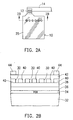
- Figs. 1A and 1B there are shown schematic diagrams of the prior art process for connecting a large contact pad with an active MOS device by using a metal layer, which could lead to device damage due to the antenna effect.
- a large contact pad area 10 (of typical size 100 by 100 micrometers, and more than about 30 by 30 micrometers) is electrically connected by vias 12 to a polysilicon interconnection 14.
- the pad area 10 in a double metal process would consist of two layers 24 and 26 of metal, as shown in Fig. 1B.
- the upper metal layer, or metal II, 26 is connected through an insulating layer 28 to the lower metal layer, or metal I, 24 by a large via 25 which is generally less than 5 micrometers of the large contact pad area 10.
- the polysilicon interconnection 14 is connected by vias 16 through an insulating layer to metal interconnection 18.
- This metal interconnection 18 is connected by vias 17 to polysilicon 20 to active devices 22.
- the induced charge can lead to damage to the devices 22 via the direct electrical connection path, from the lower metal layer 24, the polysilicon interconnection 14, the metal interconnection 18 to the polysilicon 20.
- the greater the size of the large via 25 is, the greater amount of the charge induced and accumulated.
- a plasma is a collection of charged particles, including electrons and positive and negative ions, and it is these charged particles that collect along the conductive surfaces during plasma processing, and may produce the trapped charges damaging the gate oxide.
- the primary object of the present invention is to provide a method that will reduce the charge that may accumulate at the gate oxide by reducing the size of the exposed contact pad area during plasma processing.
- a method of forming large contact pad areas for interconnection to an integrated circuit in a silicon substrate comprises: forming a first layer of metal on the substrate; forming an insulating layer over the first metal layer; forming at least one opening to the first metal layer through the insulating layer, such that the exposed area of the first metal layer through the opening is effectively small; processing in a plasma environment that would normally produce electrical charge build-up at the gate oxide of the integrated circuit, but wherein the effectively small area of the exposed first metal layer reduces the charge build-up; forming a second layer of metal to form the large contact pad areas, such that the second metal layer electrically connects to the first metal layer through the opening in the insulating layer; and forming a passivation layer over the second metal layer.
- the first metal layer is much smaller than the large contact pad area in order to further reduce the charge build-up at the gate oxide of the integrated circuit.
- the size of the first metal layer is about 6 ⁇ 100 micrometers, and the size of the large contact pad area is about 80 ⁇ 80 to 200 ⁇ 200 micrometers.
- the large contact pad areas are located at the periphery of the integrated circuit.
- the processing in a plasma environment is plasma enhanced chemical vapor deposition, plasma etching or sputter etch.
- the second metal layer is formed to be the same size as the first metal layer, and the method further comprises the steps of further processing in a plasma environment that would normally produce electrical charge build-up at the gate oxide of the integrated circuit, but wherein the small second metal layer reduces the charge build-up; forming a second insulating layer over the second metal layer; forming at least one opening to the second metal layer through the second insulating layer; forming a third layer of metal to form the large contact pad areas, such that the third metal layer electrically connects to the second metal layer through the opening in the second insulating layer; and forming a passivation layer over the third metal layer. Additional metal layers could be formed in a similar way.
- the method further comprises the steps of forming a second insulating layer over the second metal layer; forming at least one opening to the second metal layer through the second insulating layer, such that the exposed area of the second metal layer through the opening in the second insulating layer is effectively small; further processing in a plasma environment that would normally produce an electrical charge build-up at the gate oxide of the integrated circuit, but wherein the effectively small area of the exposed second metal layer reduces the charge build-up; forming a third layer of metal to form the large contact pad areas, such that the third metal layer electrically connects to the second metal layer through the opening in the second insulating layer; and forming a passivation layer over the third metal layer. Additional metal layers could be formed in a similar way.
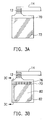
- Fig. 2A there is shown the preferred embodiment of the present invention.
- This embodiment is very similar to the prior art as shown in Fig. 1A.
- the only difference is that the present invention substitutes six small vias 30 for the single large via 25 of Fig. 1A.
- the small vias 30 would expose a smaller area of metal I than the large via 25 does.
- the reduced area of exposed metal I will lessen any charge accumulated during plasma processing.
- the size of the vias 30 is about 2 ⁇ 2 micrometers.
- the number and size of the vias 30 are not intended to be limited to those described above. According to the present invention, the antenna effect can be effectively reduced so long as the exposed area of metal I is effectively decreased.
- FIG. 2B there is shown a cross-sectional representation of the embodiment shown in Fig. 2A.
- Field oxide (FOX) 34 is thermally grown on substrate 32, and BPSG (Borophosilicate glass) insulating layer 36 is deposited on FOX 34.
- First metal layer 38 is deposited and patterned, and then another insulating layer 40 is formed.
- Vias 30 are opened by lithography and etching through the insulating layer 40. The size of the vias 30 is effectively decreased to minimize charge accumulation during plasma processing steps, so that the antenna effect is effectively reduced.
- Second metal layer 42 is then deposited and connected to the first metal layer 38.
- Passivation layer 44 is deposited over the second metal layer 42.
- First metal layer 70 is deposited and patterned by conventional lithography and etching to cover a much smaller area than the eventual large contact pad area 72.
- the actual typical dimension of the much smaller area is about 6 ⁇ 100 micrometers, whereas the dimension of the larger contact pad area is between about 80 ⁇ 80 and 200 ⁇ 200 micrometers.
- the reduced area of metal I will further lessen any charge accumulated thereon during subsequent plasma processing.
- the first metal layer 70 is connected to the polysilicon interconnection 14 through the vias 12.
- second metal layer 80 is formed and connected to the first metal layer 70 through some small size vias 76, in order to reduce the sputter etch damage before metal II sputtering.
- the via size is, for example, about 2 ⁇ 2 micrometers.
- Passivation layer 82 is formed on top of second metal layer 80, around the perimeter of the contact pad.
- FIG. 3C there is shown a cross-sectional representation of the embodiment shown in Fig. 3B.
- Field oxide 90 is thermally grown on substrate 50, and BPSG insulating layer 92 is deposited on FOX 90.
- First metal layer 70 is deposited and patterned to be a much reduced area compared to the large contact pad area. This smaller area minimizes charge accumulation during subsequent plasma processing steps.
- Second metal layer 80 is deposited and connected to the first metal layer 70, and comprises the complete and much larger pad area than metal I 70. Passivation layer 82 is deposited over the second metal layer 80.
- FIG. 4 there is shown a cross-sectional representation of the formation of a contact pad in a three-metal technology.
- Field oxide 90 is grown on substrate 50, and BPSG insulating layer 92 is deposited on FOX 90.
- First metal layr 70 is deposited to be a much reduced area compared to the large contact pad area. This smaller area minimizes charge accumulation during subsequent plasma processing steps.
- Second metal layer 80 is deposited and patterned to be the same size as the first metal layer 70, and connected to the first metal layer 70. Further plasma processing may take place with minimal charge accumulation.
- Third metal layer 110 is deposited and connected to the second metal layer 80, and comprises the complete pad area. Passivation layer 112 is deposited over the third metal layer 110.
Landscapes
- Internal Circuitry In Semiconductor Integrated Circuit Devices (AREA)
- Insulated Gate Type Field-Effect Transistor (AREA)
Priority Applications (2)
| Application Number | Priority Date | Filing Date | Title |
|---|---|---|---|
| EP94305121A EP0693782B1 (fr) | 1994-07-13 | 1994-07-13 | Procédé pour la réduction de l'effet d'antenne pendant la fabrication |
| DE69426293T DE69426293T2 (de) | 1994-07-13 | 1994-07-13 | Verfahren zur Reduzierung des Antenneneffekts während der Fabrikation |
Applications Claiming Priority (1)
| Application Number | Priority Date | Filing Date | Title |
|---|---|---|---|
| EP94305121A EP0693782B1 (fr) | 1994-07-13 | 1994-07-13 | Procédé pour la réduction de l'effet d'antenne pendant la fabrication |
Publications (2)
| Publication Number | Publication Date |
|---|---|
| EP0693782A1 true EP0693782A1 (fr) | 1996-01-24 |
| EP0693782B1 EP0693782B1 (fr) | 2000-11-15 |
Family
ID=8217767
Family Applications (1)
| Application Number | Title | Priority Date | Filing Date |
|---|---|---|---|
| EP94305121A Expired - Lifetime EP0693782B1 (fr) | 1994-07-13 | 1994-07-13 | Procédé pour la réduction de l'effet d'antenne pendant la fabrication |
Country Status (2)
| Country | Link |
|---|---|
| EP (1) | EP0693782B1 (fr) |
| DE (1) | DE69426293T2 (fr) |
Cited By (1)
| Publication number | Priority date | Publication date | Assignee | Title |
|---|---|---|---|---|
| EP1154477A1 (fr) * | 2000-05-11 | 2001-11-14 | Infineon Technologies AG | Plot de contact pour dispositif semi-conducteur |
Citations (9)
| Publication number | Priority date | Publication date | Assignee | Title |
|---|---|---|---|---|
| JPS5898938A (ja) * | 1981-12-09 | 1983-06-13 | Nec Corp | 半導体集積回路 |
| JPS6045048A (ja) * | 1983-08-22 | 1985-03-11 | Nec Corp | 半導体装置 |
| JPS61154054A (ja) * | 1984-12-26 | 1986-07-12 | Toshiba Corp | 半導体装置 |
| JPS61172362A (ja) * | 1985-01-28 | 1986-08-04 | Seiko Epson Corp | ボンデイング電極構造 |
| GB2174543A (en) * | 1985-04-26 | 1986-11-05 | Sgs Microelettronica Spa | Improved packaging of semiconductor devices |
| EP0291014A2 (fr) * | 1987-05-15 | 1988-11-17 | Kabushiki Kaisha Toshiba | Dispositif semi-conducteur comprenant une couche conductrice au-dessous de la plage de contact |
| US4941028A (en) * | 1988-08-10 | 1990-07-10 | Actel Corporation | Structure for protecting thin dielectrics during processing |
| EP0431490A1 (fr) * | 1989-12-02 | 1991-06-12 | Kabushiki Kaisha Toshiba | Dispositif de circuit intégré semi-conducteur comprenant des plats de jonction à la périphÀ©rie de la puce semi-conductrice |
| EP0490506A1 (fr) * | 1990-11-24 | 1992-06-17 | Nec Corporation | Dispositif semiconducteur comprenant une plage de contact |
Family Cites Families (1)
| Publication number | Priority date | Publication date | Assignee | Title |
|---|---|---|---|---|
| DE69321106T2 (de) * | 1993-06-28 | 1999-02-25 | Stmicroelectronics S.R.L., Agrate Brianza, Mailand/Milano | Integriertes Bauelement mit Mehrschichtmetallisierung und Herstellungsverfahren |
-
1994
- 1994-07-13 EP EP94305121A patent/EP0693782B1/fr not_active Expired - Lifetime
- 1994-07-13 DE DE69426293T patent/DE69426293T2/de not_active Expired - Lifetime
Patent Citations (9)
| Publication number | Priority date | Publication date | Assignee | Title |
|---|---|---|---|---|
| JPS5898938A (ja) * | 1981-12-09 | 1983-06-13 | Nec Corp | 半導体集積回路 |
| JPS6045048A (ja) * | 1983-08-22 | 1985-03-11 | Nec Corp | 半導体装置 |
| JPS61154054A (ja) * | 1984-12-26 | 1986-07-12 | Toshiba Corp | 半導体装置 |
| JPS61172362A (ja) * | 1985-01-28 | 1986-08-04 | Seiko Epson Corp | ボンデイング電極構造 |
| GB2174543A (en) * | 1985-04-26 | 1986-11-05 | Sgs Microelettronica Spa | Improved packaging of semiconductor devices |
| EP0291014A2 (fr) * | 1987-05-15 | 1988-11-17 | Kabushiki Kaisha Toshiba | Dispositif semi-conducteur comprenant une couche conductrice au-dessous de la plage de contact |
| US4941028A (en) * | 1988-08-10 | 1990-07-10 | Actel Corporation | Structure for protecting thin dielectrics during processing |
| EP0431490A1 (fr) * | 1989-12-02 | 1991-06-12 | Kabushiki Kaisha Toshiba | Dispositif de circuit intégré semi-conducteur comprenant des plats de jonction à la périphÀ©rie de la puce semi-conductrice |
| EP0490506A1 (fr) * | 1990-11-24 | 1992-06-17 | Nec Corporation | Dispositif semiconducteur comprenant une plage de contact |
Non-Patent Citations (4)
| Title |
|---|
| PATENT ABSTRACTS OF JAPAN vol. 10, no. 356 (E - 459) 29 November 1986 (1986-11-29) * |
| PATENT ABSTRACTS OF JAPAN vol. 10, no. 379 (E - 465) 18 December 1986 (1986-12-18) * |
| PATENT ABSTRACTS OF JAPAN vol. 7, no. 200 (E - 196) 3 September 1983 (1983-09-03) * |
| PATENT ABSTRACTS OF JAPAN vol. 9, no. 173 (E - 329) 18 July 1985 (1985-07-18) * |
Cited By (2)
| Publication number | Priority date | Publication date | Assignee | Title |
|---|---|---|---|---|
| EP1154477A1 (fr) * | 2000-05-11 | 2001-11-14 | Infineon Technologies AG | Plot de contact pour dispositif semi-conducteur |
| WO2001086720A1 (fr) * | 2000-05-11 | 2001-11-15 | Infineon Technologies Ag | Connexion a contact d'un composant semi-conducteur |
Also Published As
| Publication number | Publication date |
|---|---|
| DE69426293T2 (de) | 2001-04-05 |
| DE69426293D1 (de) | 2000-12-21 |
| EP0693782B1 (fr) | 2000-11-15 |
Similar Documents
| Publication | Publication Date | Title |
|---|---|---|
| US5514623A (en) | Method of making layout design to eliminate process antenna effect | |
| US5817577A (en) | Grounding method for eliminating process antenna effect | |
| US5350710A (en) | Device for preventing antenna effect on circuit | |
| US7160786B2 (en) | Silicon on insulator device and layout method of the same | |
| US5369054A (en) | Circuits for ESD protection of metal-to-metal antifuses during processing | |
| JP4002647B2 (ja) | 半導体素子の薄膜キャパシタ製造方法 | |
| US5319246A (en) | Semiconductor device having multi-layer film structure | |
| US5691234A (en) | Buried contact method to release plasma-induced charging damage on device | |
| US5188970A (en) | Method for forming an infrared detector having a refractory metal | |
| US6150261A (en) | Method of fabricating semiconductor device for preventing antenna effect | |
| JPH10189501A (ja) | プラズマ損傷の抑制のための保護構造の方法 | |
| US20020000579A1 (en) | Semiconductor device having a gate insulation film resistant to dielectric breakdown. | |
| US5434108A (en) | Grounding method to eliminate the antenna effect in VLSI process | |
| KR100418644B1 (ko) | 반도체장치 및 그의 제조방법 | |
| JP3864295B2 (ja) | 半導体素子及びその製造方法 | |
| JP3897339B2 (ja) | Soiデバイスのプラズマ・チャージング損傷を最小化する構造および方法 | |
| EP0693782A1 (fr) | Procédé pour la réduction de l'effet d'antenne pendant la fabrication | |
| EP0693783A1 (fr) | Procédé pour l'élimination de l'effet d'antenne pendant la fabrication | |
| EP0110656B1 (fr) | Dispositif semi-conducteur et son procédé de fabrication | |
| JP3129703B2 (ja) | Mosトランジスタを備えた半導体装置及びその製造方法 | |
| US20050236658A1 (en) | Semiconductor device and production method therefor | |
| EP0631314A1 (fr) | Dispositif intégré à niveaux métalliques multiples et procédé de fabrication | |
| US5132761A (en) | Method and apparatus for forming an infrared detector having a refractory metal | |
| JPH07321118A (ja) | 半導体装置の配線形成方法 | |
| JPH0587137B2 (fr) |
Legal Events
| Date | Code | Title | Description |
|---|---|---|---|
| PUAI | Public reference made under article 153(3) epc to a published international application that has entered the european phase |
Free format text: ORIGINAL CODE: 0009012 |
|
| 17P | Request for examination filed |
Effective date: 19940804 |
|
| AK | Designated contracting states |
Kind code of ref document: A1 Designated state(s): DE FR GB IT NL |
|
| 17Q | First examination report despatched |
Effective date: 19970901 |
|
| GRAG | Despatch of communication of intention to grant |
Free format text: ORIGINAL CODE: EPIDOS AGRA |
|
| GRAG | Despatch of communication of intention to grant |
Free format text: ORIGINAL CODE: EPIDOS AGRA |
|
| GRAH | Despatch of communication of intention to grant a patent |
Free format text: ORIGINAL CODE: EPIDOS IGRA |
|
| GRAH | Despatch of communication of intention to grant a patent |
Free format text: ORIGINAL CODE: EPIDOS IGRA |
|
| GRAA | (expected) grant |
Free format text: ORIGINAL CODE: 0009210 |
|
| AK | Designated contracting states |
Kind code of ref document: B1 Designated state(s): DE FR GB IT NL |
|
| ITF | It: translation for a ep patent filed | ||
| REF | Corresponds to: |
Ref document number: 69426293 Country of ref document: DE Date of ref document: 20001221 |
|
| ET | Fr: translation filed | ||
| PLBE | No opposition filed within time limit |
Free format text: ORIGINAL CODE: 0009261 |
|
| STAA | Information on the status of an ep patent application or granted ep patent |
Free format text: STATUS: NO OPPOSITION FILED WITHIN TIME LIMIT |
|
| 26N | No opposition filed | ||
| REG | Reference to a national code |
Ref country code: GB Ref legal event code: IF02 |
|
| PGFP | Annual fee paid to national office [announced via postgrant information from national office to epo] |
Ref country code: GB Payment date: 20130624 Year of fee payment: 20 |
|
| PGFP | Annual fee paid to national office [announced via postgrant information from national office to epo] |
Ref country code: NL Payment date: 20130716 Year of fee payment: 20 Ref country code: DE Payment date: 20130711 Year of fee payment: 20 |
|
| PGFP | Annual fee paid to national office [announced via postgrant information from national office to epo] |
Ref country code: FR Payment date: 20130724 Year of fee payment: 20 |
|
| PGFP | Annual fee paid to national office [announced via postgrant information from national office to epo] |
Ref country code: IT Payment date: 20130718 Year of fee payment: 20 |
|
| REG | Reference to a national code |
Ref country code: DE Ref legal event code: R071 Ref document number: 69426293 Country of ref document: DE |
|
| REG | Reference to a national code |
Ref country code: DE Ref legal event code: R071 Ref document number: 69426293 Country of ref document: DE |
|
| REG | Reference to a national code |
Ref country code: NL Ref legal event code: V4 Effective date: 20140713 |
|
| REG | Reference to a national code |
Ref country code: GB Ref legal event code: PE20 Expiry date: 20140712 |
|
| PG25 | Lapsed in a contracting state [announced via postgrant information from national office to epo] |
Ref country code: DE Free format text: LAPSE BECAUSE OF EXPIRATION OF PROTECTION Effective date: 20140715 |
|
| PG25 | Lapsed in a contracting state [announced via postgrant information from national office to epo] |
Ref country code: GB Free format text: LAPSE BECAUSE OF EXPIRATION OF PROTECTION Effective date: 20140712 |