EP0698920A2 - Ein Verfahren zum Montieren integrierter Schaltungen auf gedruckten Schaltungsplatten - Google Patents
Ein Verfahren zum Montieren integrierter Schaltungen auf gedruckten Schaltungsplatten Download PDFInfo
- Publication number
- EP0698920A2 EP0698920A2 EP95830366A EP95830366A EP0698920A2 EP 0698920 A2 EP0698920 A2 EP 0698920A2 EP 95830366 A EP95830366 A EP 95830366A EP 95830366 A EP95830366 A EP 95830366A EP 0698920 A2 EP0698920 A2 EP 0698920A2
- Authority
- EP
- European Patent Office
- Prior art keywords
- chip
- printed circuit
- circuit board
- adhesive
- slots
- Prior art date
- Legal status (The legal status is an assumption and is not a legal conclusion. Google has not performed a legal analysis and makes no representation as to the accuracy of the status listed.)
- Withdrawn
Links
Images


Classifications
-
- H—ELECTRICITY
- H10—SEMICONDUCTOR DEVICES; ELECTRIC SOLID-STATE DEVICES NOT OTHERWISE PROVIDED FOR
- H10W—GENERIC PACKAGES, INTERCONNECTIONS, CONNECTORS OR OTHER CONSTRUCTIONAL DETAILS OF DEVICES COVERED BY CLASS H10
- H10W74/00—Encapsulations, e.g. protective coatings
- H10W74/10—Encapsulations, e.g. protective coatings characterised by their shape or disposition
- H10W74/111—Encapsulations, e.g. protective coatings characterised by their shape or disposition the semiconductor body being completely enclosed
- H10W74/114—Encapsulations, e.g. protective coatings characterised by their shape or disposition the semiconductor body being completely enclosed by a substrate and the encapsulations
-
- H—ELECTRICITY
- H10—SEMICONDUCTOR DEVICES; ELECTRIC SOLID-STATE DEVICES NOT OTHERWISE PROVIDED FOR
- H10W—GENERIC PACKAGES, INTERCONNECTIONS, CONNECTORS OR OTHER CONSTRUCTIONAL DETAILS OF DEVICES COVERED BY CLASS H10
- H10W70/00—Package substrates; Interposers; Redistribution layers [RDL]
- H10W70/40—Leadframes
- H10W70/411—Chip-supporting parts, e.g. die pads
- H10W70/415—Leadframe inner leads serving as die pads
-
- H—ELECTRICITY
- H10—SEMICONDUCTOR DEVICES; ELECTRIC SOLID-STATE DEVICES NOT OTHERWISE PROVIDED FOR
- H10W—GENERIC PACKAGES, INTERCONNECTIONS, CONNECTORS OR OTHER CONSTRUCTIONAL DETAILS OF DEVICES COVERED BY CLASS H10
- H10W72/00—Interconnections or connectors in packages
- H10W72/01—Manufacture or treatment
- H10W72/0198—Manufacture or treatment batch processes
-
- H—ELECTRICITY
- H10—SEMICONDUCTOR DEVICES; ELECTRIC SOLID-STATE DEVICES NOT OTHERWISE PROVIDED FOR
- H10W—GENERIC PACKAGES, INTERCONNECTIONS, CONNECTORS OR OTHER CONSTRUCTIONAL DETAILS OF DEVICES COVERED BY CLASS H10
- H10W72/00—Interconnections or connectors in packages
- H10W72/071—Connecting or disconnecting
- H10W72/073—Connecting or disconnecting of die-attach connectors
-
- H—ELECTRICITY
- H10—SEMICONDUCTOR DEVICES; ELECTRIC SOLID-STATE DEVICES NOT OTHERWISE PROVIDED FOR
- H10W—GENERIC PACKAGES, INTERCONNECTIONS, CONNECTORS OR OTHER CONSTRUCTIONAL DETAILS OF DEVICES COVERED BY CLASS H10
- H10W72/00—Interconnections or connectors in packages
- H10W72/071—Connecting or disconnecting
- H10W72/073—Connecting or disconnecting of die-attach connectors
- H10W72/07351—Connecting or disconnecting of die-attach connectors characterised by changes in properties of the die-attach connectors during connecting
- H10W72/07352—Connecting or disconnecting of die-attach connectors characterised by changes in properties of the die-attach connectors during connecting changes in structures or sizes
-
- H—ELECTRICITY
- H10—SEMICONDUCTOR DEVICES; ELECTRIC SOLID-STATE DEVICES NOT OTHERWISE PROVIDED FOR
- H10W—GENERIC PACKAGES, INTERCONNECTIONS, CONNECTORS OR OTHER CONSTRUCTIONAL DETAILS OF DEVICES COVERED BY CLASS H10
- H10W72/00—Interconnections or connectors in packages
- H10W72/071—Connecting or disconnecting
- H10W72/075—Connecting or disconnecting of bond wires
-
- H—ELECTRICITY
- H10—SEMICONDUCTOR DEVICES; ELECTRIC SOLID-STATE DEVICES NOT OTHERWISE PROVIDED FOR
- H10W—GENERIC PACKAGES, INTERCONNECTIONS, CONNECTORS OR OTHER CONSTRUCTIONAL DETAILS OF DEVICES COVERED BY CLASS H10
- H10W72/00—Interconnections or connectors in packages
- H10W72/30—Die-attach connectors
- H10W72/321—Structures or relative sizes of die-attach connectors
-
- H—ELECTRICITY
- H10—SEMICONDUCTOR DEVICES; ELECTRIC SOLID-STATE DEVICES NOT OTHERWISE PROVIDED FOR
- H10W—GENERIC PACKAGES, INTERCONNECTIONS, CONNECTORS OR OTHER CONSTRUCTIONAL DETAILS OF DEVICES COVERED BY CLASS H10
- H10W72/00—Interconnections or connectors in packages
- H10W72/50—Bond wires
- H10W72/531—Shapes of wire connectors
- H10W72/536—Shapes of wire connectors the connected ends being ball-shaped
-
- H—ELECTRICITY
- H10—SEMICONDUCTOR DEVICES; ELECTRIC SOLID-STATE DEVICES NOT OTHERWISE PROVIDED FOR
- H10W—GENERIC PACKAGES, INTERCONNECTIONS, CONNECTORS OR OTHER CONSTRUCTIONAL DETAILS OF DEVICES COVERED BY CLASS H10
- H10W72/00—Interconnections or connectors in packages
- H10W72/50—Bond wires
- H10W72/531—Shapes of wire connectors
- H10W72/5363—Shapes of wire connectors the connected ends being wedge-shaped
-
- H—ELECTRICITY
- H10—SEMICONDUCTOR DEVICES; ELECTRIC SOLID-STATE DEVICES NOT OTHERWISE PROVIDED FOR
- H10W—GENERIC PACKAGES, INTERCONNECTIONS, CONNECTORS OR OTHER CONSTRUCTIONAL DETAILS OF DEVICES COVERED BY CLASS H10
- H10W72/00—Interconnections or connectors in packages
- H10W72/50—Bond wires
- H10W72/551—Materials of bond wires
- H10W72/552—Materials of bond wires comprising metals or metalloids, e.g. silver
- H10W72/5522—Materials of bond wires comprising metals or metalloids, e.g. silver comprising gold [Au]
-
- H—ELECTRICITY
- H10—SEMICONDUCTOR DEVICES; ELECTRIC SOLID-STATE DEVICES NOT OTHERWISE PROVIDED FOR
- H10W—GENERIC PACKAGES, INTERCONNECTIONS, CONNECTORS OR OTHER CONSTRUCTIONAL DETAILS OF DEVICES COVERED BY CLASS H10
- H10W72/00—Interconnections or connectors in packages
- H10W72/50—Bond wires
- H10W72/551—Materials of bond wires
- H10W72/552—Materials of bond wires comprising metals or metalloids, e.g. silver
- H10W72/5524—Materials of bond wires comprising metals or metalloids, e.g. silver comprising aluminium [Al]
-
- H—ELECTRICITY
- H10—SEMICONDUCTOR DEVICES; ELECTRIC SOLID-STATE DEVICES NOT OTHERWISE PROVIDED FOR
- H10W—GENERIC PACKAGES, INTERCONNECTIONS, CONNECTORS OR OTHER CONSTRUCTIONAL DETAILS OF DEVICES COVERED BY CLASS H10
- H10W72/00—Interconnections or connectors in packages
- H10W72/851—Dispositions of multiple connectors or interconnections
- H10W72/853—On the same surface
- H10W72/865—Die-attach connectors and bond wires
-
- H—ELECTRICITY
- H10—SEMICONDUCTOR DEVICES; ELECTRIC SOLID-STATE DEVICES NOT OTHERWISE PROVIDED FOR
- H10W—GENERIC PACKAGES, INTERCONNECTIONS, CONNECTORS OR OTHER CONSTRUCTIONAL DETAILS OF DEVICES COVERED BY CLASS H10
- H10W90/00—Package configurations
- H10W90/701—Package configurations characterised by the relative positions of pads or connectors relative to package parts
- H10W90/731—Package configurations characterised by the relative positions of pads or connectors relative to package parts of die-attach connectors
- H10W90/734—Package configurations characterised by the relative positions of pads or connectors relative to package parts of die-attach connectors between a chip and a stacked insulating package substrate, interposer or RDL
-
- H—ELECTRICITY
- H10—SEMICONDUCTOR DEVICES; ELECTRIC SOLID-STATE DEVICES NOT OTHERWISE PROVIDED FOR
- H10W—GENERIC PACKAGES, INTERCONNECTIONS, CONNECTORS OR OTHER CONSTRUCTIONAL DETAILS OF DEVICES COVERED BY CLASS H10
- H10W90/00—Package configurations
- H10W90/701—Package configurations characterised by the relative positions of pads or connectors relative to package parts
- H10W90/751—Package configurations characterised by the relative positions of pads or connectors relative to package parts of bond wires
- H10W90/754—Package configurations characterised by the relative positions of pads or connectors relative to package parts of bond wires between a chip and a stacked insulating package substrate, interposer or RDL
-
- H—ELECTRICITY
- H10—SEMICONDUCTOR DEVICES; ELECTRIC SOLID-STATE DEVICES NOT OTHERWISE PROVIDED FOR
- H10W—GENERIC PACKAGES, INTERCONNECTIONS, CONNECTORS OR OTHER CONSTRUCTIONAL DETAILS OF DEVICES COVERED BY CLASS H10
- H10W99/00—Subject matter not provided for in other groups of this subclass
Definitions
- This invention broadly relates to manufacturing printed circuits incorporating also integrated circuits in their carrier boards.
- this invention relates to a method for assembling, connecting and packaging integrated circuit chips, for instance memory chips under a board carrying an interconnection printed circuit.
- the integrated circuit chips regardless of their function, have been manufactured upon silicon wafers and with bonding pads for connection with the external world peripherally arranged to the chips themselves.
- the concerned chip therefore, was mounted upon a frame of contact pins, the so-called lead frame, and the connection pads were connected to said contact pins by means of aluminium or gold metal wires, the function of which was to connect the chip to the printed circuit of the board.
- the chip and the lead frame, except for said connection pins were packaged in a resin casing (package) which acted as an electrical and mechanical protection for the chip.
- the first approach is the so-called LOC (Lead-On-Chip) process, wherein a particular arrangement of the bonding pads is exploited, namely the bonding pads are not peripherally arranged according to the conventional patterns, but they are centrally arranged along the main longitudinal axis of the chip. In such an arrangement, therefore, it is a requirement that the metal conductors (leads) of the containment package be positioned on the chip itself (wherefrom the term Lead-On-Chip derives).
- LOC Lead-On-Chip
- COB Chip-On-Board
- this invention consists in mounting the chip, for instance a memory chip, as above mentioned, by utilizing suitable mounting means, on the lower side of the printed circuit board acting as an interconnection means with the external world, in effecting the interconnections between the chip and said printed circuit and in locally packaging the chip with a protective resin.
- a chip adapted to the LOC process be used, namely a chip having its connection or bonding pads in central position, arranged along the longitudinal axis thereof, and that the support printed circuit board be made so as to have through slots corresponding to the chip area (main axis) along which the contact or bonding pads are arranged.
- Subject-matter of this invention is a method that, starting from the above mentioned conditions, comprises the following essential steps:
- the assembled chip when, as a result of the test steps, the assembled chip turns out to be defective, it can be removed from the printed circuit board by beating the biadhesive thermoplastic tape to a temperature higher than the softening temperature and it can be subsequently replaced by a new chip; after this step, the above mentioned ii. and iii. steps are repeated, until the result of the test is positive, and then steps iv., v and vi are carried out.
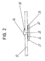
- the method according to this invention includes, as preliminary preparatory steps, (a) providing chips 10 adapted to LOC process and, as such, having bonding pads 11 aligned along the main longitudinal axis thereof and (b) providing, in the printed circuit board 12 upon which said chips 10 are to be mounted, elongated slots or grooves 13, closely corresponding to the assembly of said contact pads 11.
- the operation method per se provides for some steps to be carried out on the lower side of the printed circuit board and other steps to be carried out on its upper side.
- the support printed circuit board can be made of FR4 type material, ceramics or like.
- the first step (i) of the method provides for applying to both sides of a said slots 13 two strips 14 and 15 of a biadhesive tape, under a which term a tape is to be meant having an adhesive composition upon both its sides.
- the biadhesive tape 14, 15 can also be differently divided or it can be used as a single item having apertures corresponding to said slots 13; it is made by a polyamide type film or similar material, coated on both sides by two layers of thermoplastic adhesive resin, so as to assure not only good adhesion properties, but heat resistance and reliability, as well.
- the second operation step of the method includes (ii) bonding said chip 10 to board 12 by means of said biadhesive tape 14, 15.
- bonding between chip 10 and biadhesive tape 14, 15 and between the latter and board 12 is carried out by a single heat pressing step in very short times.
- connection step (iii) is carried out between the individual contact pads 11 of the chip and the corresponding connection pads of the printed circuit board 12, provided adjacent to said slot 13.
- the connection are extended through slot 13 of the board 12 and are carried out by means of conventional techniques, for instance a thermocompression gold wire (ball-bonding) technique or the ultrasound aluminium wire (wedge-bonding) technique.
- the connection filaments are designated as 18 in the drawings.
- the concerned chip Upon completing the bonding steps, the concerned chip can be subjected to electric tests.
- thermoplastic character of the adhesive employed enables any faulty chip to be easily removed and replaced by simple heating and subsequent pressing operations so as to allow reworking steps to be carried out before starting subsequent steps of the method, thereby avoiding any need to reject a whole printed circuit board together with all chips mounted thereupon, as it occurs at present, even when a single faulty chip is found, since the tests can be carried out only when the assembling steps of all chips have been completed.
- thermoplastic adhesive material be chosen having a softening temperature sufficiently higher than the oven temperature.
- a protective resin coating 16 is applied (step iv) upon the upper side of board 12, within slots 13 and on any connections made there through, and then a protective resin coating 17 is applied (step v) upon the lower side of the board so as to package the whole chip.
- This final packaging that eliminates any need to employ protective casings of any kind, is carried out by means of well known liquid resins, particularly suitable for use with semiconductors, which are subsequently polymerised (vi) in oven, so as to guarantee the necessary rigidity and mechanical protection, in addition to heat dissipation and humidity resistance properties.
- the end product is shown in partial cross-section view in Figure 2.
- FIG. 3 the application of the method according to this invention is shown in Figure 3, for manufacturing a memory module, namely an assembly of memory chips directly mounted on the lower side of a suitable printed circuit board of " FR4 glass-filled” type, as designed for use as an expansion of the basic memory of a Personal Computer.
Landscapes
- Wire Bonding (AREA)
- Combinations Of Printed Boards (AREA)
- Structures For Mounting Electric Components On Printed Circuit Boards (AREA)
- Encapsulation Of And Coatings For Semiconductor Or Solid State Devices (AREA)
Applications Claiming Priority (2)
| Application Number | Priority Date | Filing Date | Title |
|---|---|---|---|
| ITRM940544 | 1994-08-24 | ||
| ITRM940544A IT1272817B (it) | 1994-08-24 | 1994-08-24 | Procedimento per il montaggio di circuiti integrati su pannelli di circuiti stampati |
Publications (2)
| Publication Number | Publication Date |
|---|---|
| EP0698920A2 true EP0698920A2 (de) | 1996-02-28 |
| EP0698920A3 EP0698920A3 (de) | 1998-01-07 |
Family
ID=11402704
Family Applications (1)
| Application Number | Title | Priority Date | Filing Date |
|---|---|---|---|
| EP95830366A Withdrawn EP0698920A3 (de) | 1994-08-24 | 1995-08-24 | Ein Verfahren zum Montieren integrierter Schaltungen auf gedruckten Schaltungsplatten |
Country Status (3)
| Country | Link |
|---|---|
| EP (1) | EP0698920A3 (de) |
| JP (1) | JPH08172254A (de) |
| IT (1) | IT1272817B (de) |
Cited By (2)
| Publication number | Priority date | Publication date | Assignee | Title |
|---|---|---|---|---|
| EP0810655A3 (de) * | 1996-05-29 | 1999-10-06 | Texas Instruments Incorporated | Eine Packung für eine Halbleiteranordnung |
| US6984894B2 (en) * | 2000-03-07 | 2006-01-10 | Micron Technology, Inc. | Semiconductor package having a partial slot cover for encapsulation process |
Families Citing this family (1)
| Publication number | Priority date | Publication date | Assignee | Title |
|---|---|---|---|---|
| JP2023139563A (ja) * | 2022-03-22 | 2023-10-04 | 日本無線株式会社 | マルチチップモジュール |
Family Cites Families (4)
| Publication number | Priority date | Publication date | Assignee | Title |
|---|---|---|---|---|
| JPS58178529A (ja) * | 1982-04-13 | 1983-10-19 | Mitsubishi Electric Corp | 混成集積回路装置 |
| DE3911711A1 (de) * | 1989-04-10 | 1990-10-11 | Ibm | Modul-aufbau mit integriertem halbleiterchip und chiptraeger |
| US5227232A (en) * | 1991-01-23 | 1993-07-13 | Lim Thiam B | Conductive tape for semiconductor package, a lead frame without power buses for lead on chip package, and a semiconductor device with conductive tape power distribution |
| US5384689A (en) * | 1993-12-20 | 1995-01-24 | Shen; Ming-Tung | Integrated circuit chip including superimposed upper and lower printed circuit boards |
-
1994
- 1994-08-24 IT ITRM940544A patent/IT1272817B/it active IP Right Grant
-
1995
- 1995-08-24 EP EP95830366A patent/EP0698920A3/de not_active Withdrawn
- 1995-08-24 JP JP7216184A patent/JPH08172254A/ja active Pending
Non-Patent Citations (1)
| Title |
|---|
| None |
Cited By (3)
| Publication number | Priority date | Publication date | Assignee | Title |
|---|---|---|---|---|
| EP0810655A3 (de) * | 1996-05-29 | 1999-10-06 | Texas Instruments Incorporated | Eine Packung für eine Halbleiteranordnung |
| US6667560B2 (en) | 1996-05-29 | 2003-12-23 | Texas Instruments Incorporated | Board on chip ball grid array |
| US6984894B2 (en) * | 2000-03-07 | 2006-01-10 | Micron Technology, Inc. | Semiconductor package having a partial slot cover for encapsulation process |
Also Published As
| Publication number | Publication date |
|---|---|
| JPH08172254A (ja) | 1996-07-02 |
| ITRM940544A0 (it) | 1994-08-24 |
| ITRM940544A1 (it) | 1996-02-24 |
| IT1272817B (it) | 1997-06-30 |
| EP0698920A3 (de) | 1998-01-07 |
Similar Documents
| Publication | Publication Date | Title |
|---|---|---|
| US6362532B1 (en) | Semiconductor device having ball-bonded pads | |
| JP2944449B2 (ja) | 半導体パッケージとその製造方法 | |
| EP2362416B1 (de) | Multichipmodul | |
| US20010006828A1 (en) | Stacked chip packaging | |
| US5854740A (en) | Electronic circuit board with semiconductor chip mounted thereon, and manufacturing method therefor | |
| JPH1093001A (ja) | 半導体パッケージおよびその製造方法 | |
| CN1153997A (zh) | 改进的减小尺寸的集成芯片封装 | |
| EP0670594A1 (de) | Halbleiterpackung und Herstellungsverfahren dafur | |
| JPH0399456A (ja) | 半導体装置およびその製造方法 | |
| JP2000299425A (ja) | 修復可能なマルチチップモジュールパッケージ | |
| US6853202B1 (en) | Non-stick detection method and mechanism for array molded laminate packages | |
| JPH0394430A (ja) | 半導体装置およびその製造方法 | |
| US6495400B1 (en) | Method of forming low profile semiconductor package | |
| US5559305A (en) | Semiconductor package having adjacently arranged semiconductor chips | |
| EP0698920A2 (de) | Ein Verfahren zum Montieren integrierter Schaltungen auf gedruckten Schaltungsplatten | |
| US5196992A (en) | Resin sealing type semiconductor device in which a very small semiconductor chip is sealed in package with resin | |
| US20040152242A1 (en) | Device package utilizing interconnect strips to make connections between package and die | |
| JPH04144142A (ja) | 半導体装置 | |
| US7015585B2 (en) | Packaged integrated circuit having wire bonds and method therefor | |
| KR102525683B1 (ko) | 클립 구조체 및 그 클립 구조체를 포함하는 반도체 패키지 | |
| EP0414257A2 (de) | Halbleiteranordnung des Harzverkapselungstyps, in dem ein sehr kleiner Halbleiterchip mit Harz versiegelt ist | |
| JPH09330962A (ja) | 半導体集積回路装置およびその製造方法 | |
| WO1999026288A1 (en) | Semiconductor device and method for manufacturing the same | |
| JPH04164359A (ja) | 混成集積回路装置 | |
| KR100419950B1 (ko) | 가용성회로기판을이용한볼그리드어레이반도체패키지의제조방법 |
Legal Events
| Date | Code | Title | Description |
|---|---|---|---|
| PUAI | Public reference made under article 153(3) epc to a published international application that has entered the european phase |
Free format text: ORIGINAL CODE: 0009012 |
|
| AK | Designated contracting states |
Kind code of ref document: A2 Designated state(s): DE FR GB IT NL |
|
| PUAL | Search report despatched |
Free format text: ORIGINAL CODE: 0009013 |
|
| AK | Designated contracting states |
Kind code of ref document: A3 Designated state(s): DE FR GB IT NL |
|
| 17P | Request for examination filed |
Effective date: 19980507 |
|
| 17Q | First examination report despatched |
Effective date: 19980826 |
|
| STAA | Information on the status of an ep patent application or granted ep patent |
Free format text: STATUS: THE APPLICATION IS DEEMED TO BE WITHDRAWN |
|
| 18D | Application deemed to be withdrawn |
Effective date: 19990205 |